

A Monte-Carlo/FDTD Study of High-Efficiency Optical Antennas for LED-Based Visible Light Communication


Abstract
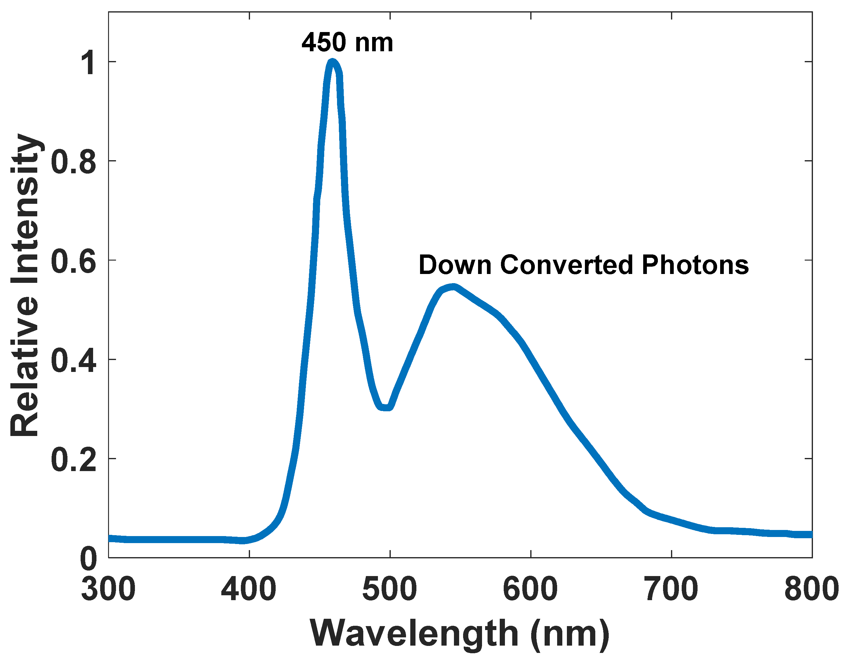
1. Introduction
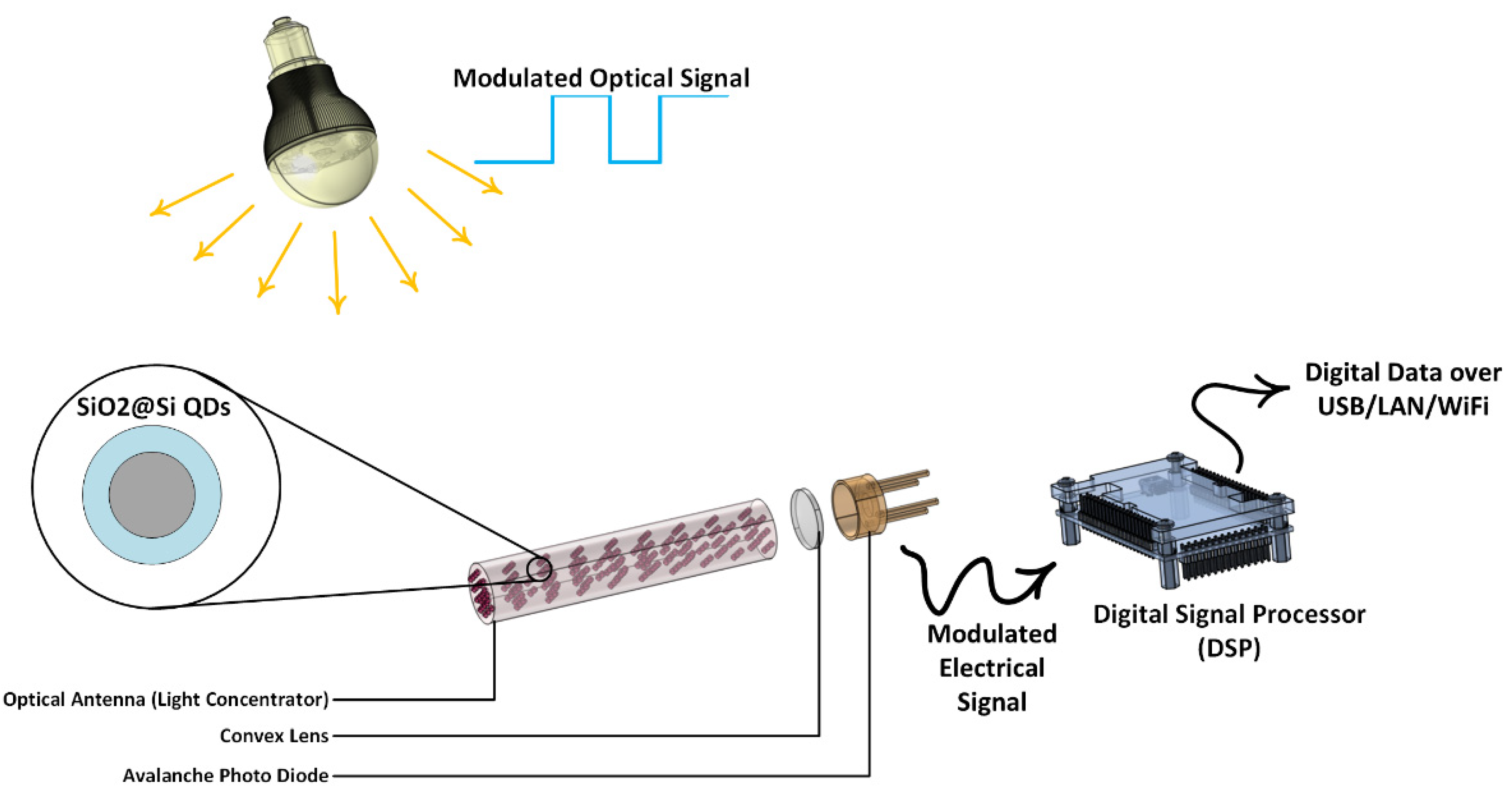
2. Materials and Methods
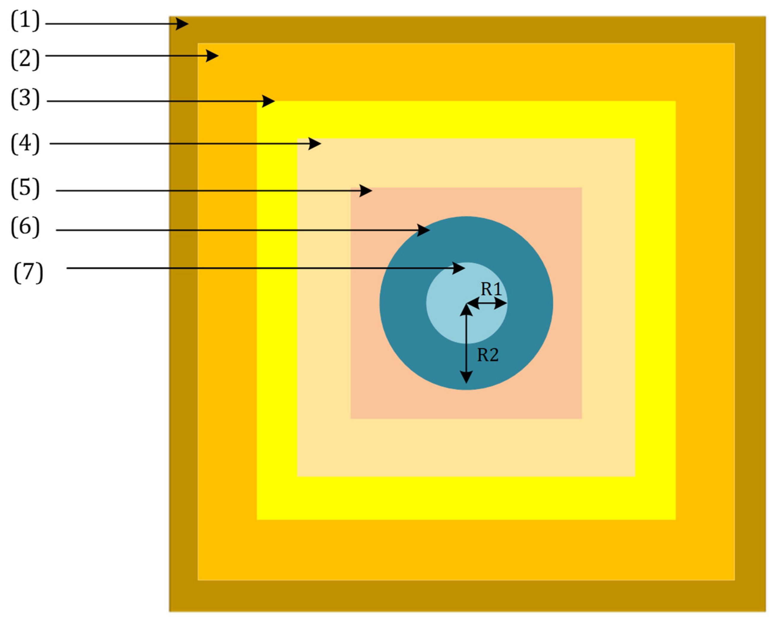
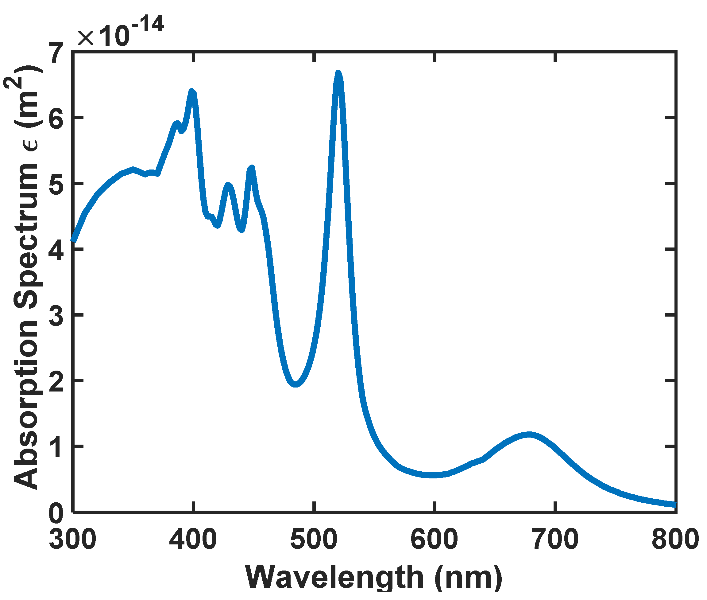
2.1. Antenna Structure and Underlying Physics
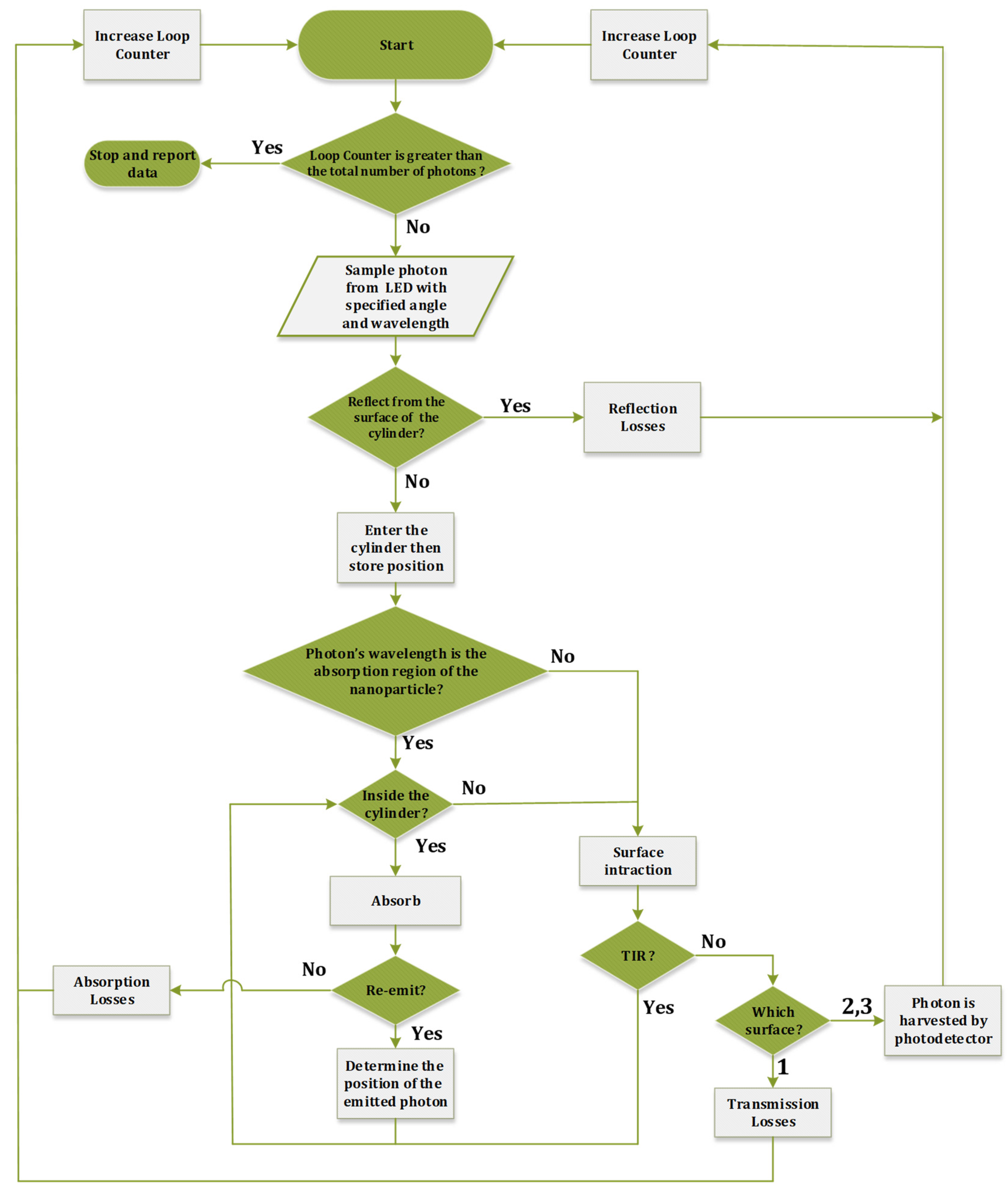
- (1)
- The photon passes through the cylinder without being absorbed by the nanoparticles (transmission losses).
- (2)
- The photon is absorbed by the nanoparticle and then is emitted and escapes from the cylinder because its incident angle with the surface is smaller than the critical angle (transmission losses).
- (3)
- The photon is absorbed by the nanoparticle and is emitted and then absorbed by another nanoparticle (re-absorption), and (3, 6) is not emitted (absorption losses). To be more precise, each photon’s absorption loss can be calculated using Equation (10).
- (4)
- The photon is absorbed by the nanoparticles and emitted and then reaches the photodetector by the TIR phenomenon.
- (5)
- The photon is reflected from the surface of the cylinder without entering it.
2.2. Simulation
2.2.1. FDTD Simulation
- Boundary conditions of the FDTD region,
- Background medium,
- Scattering calculation region,
- Planar light source,
- Absorption calculation region,
- Shell material, and
- Core material.
2.2.2. Monte Carlo Simulation
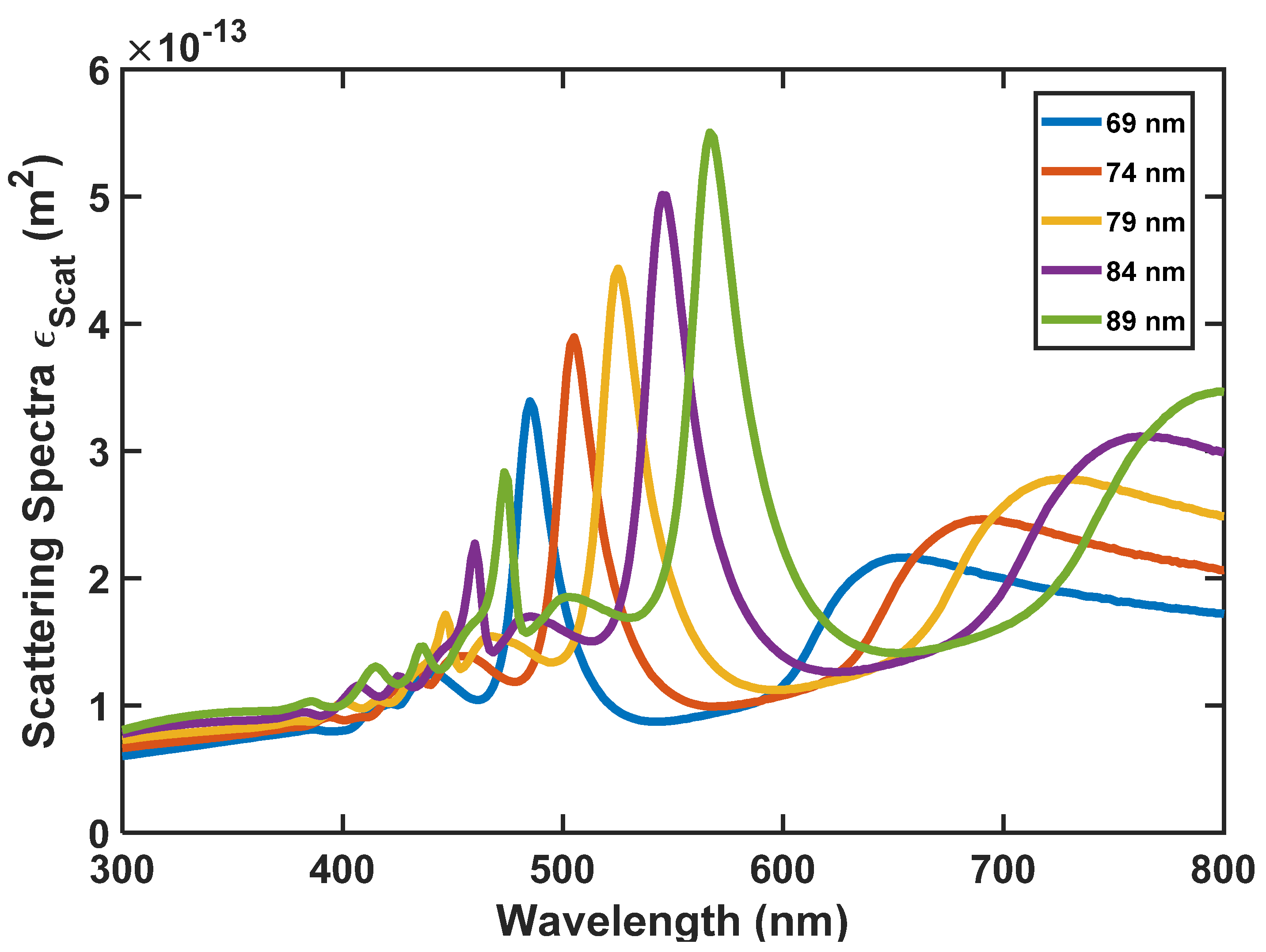
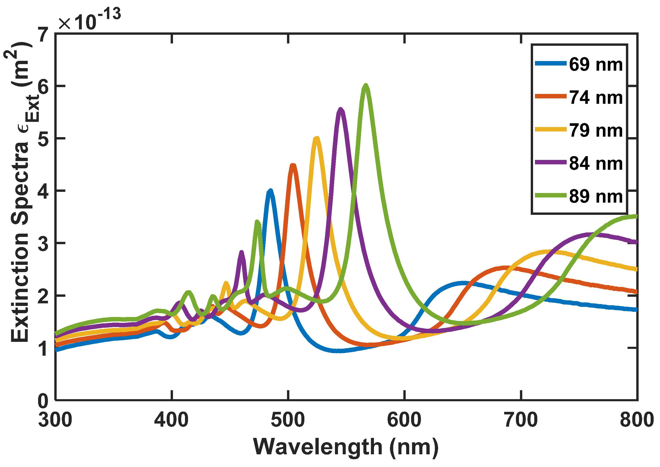
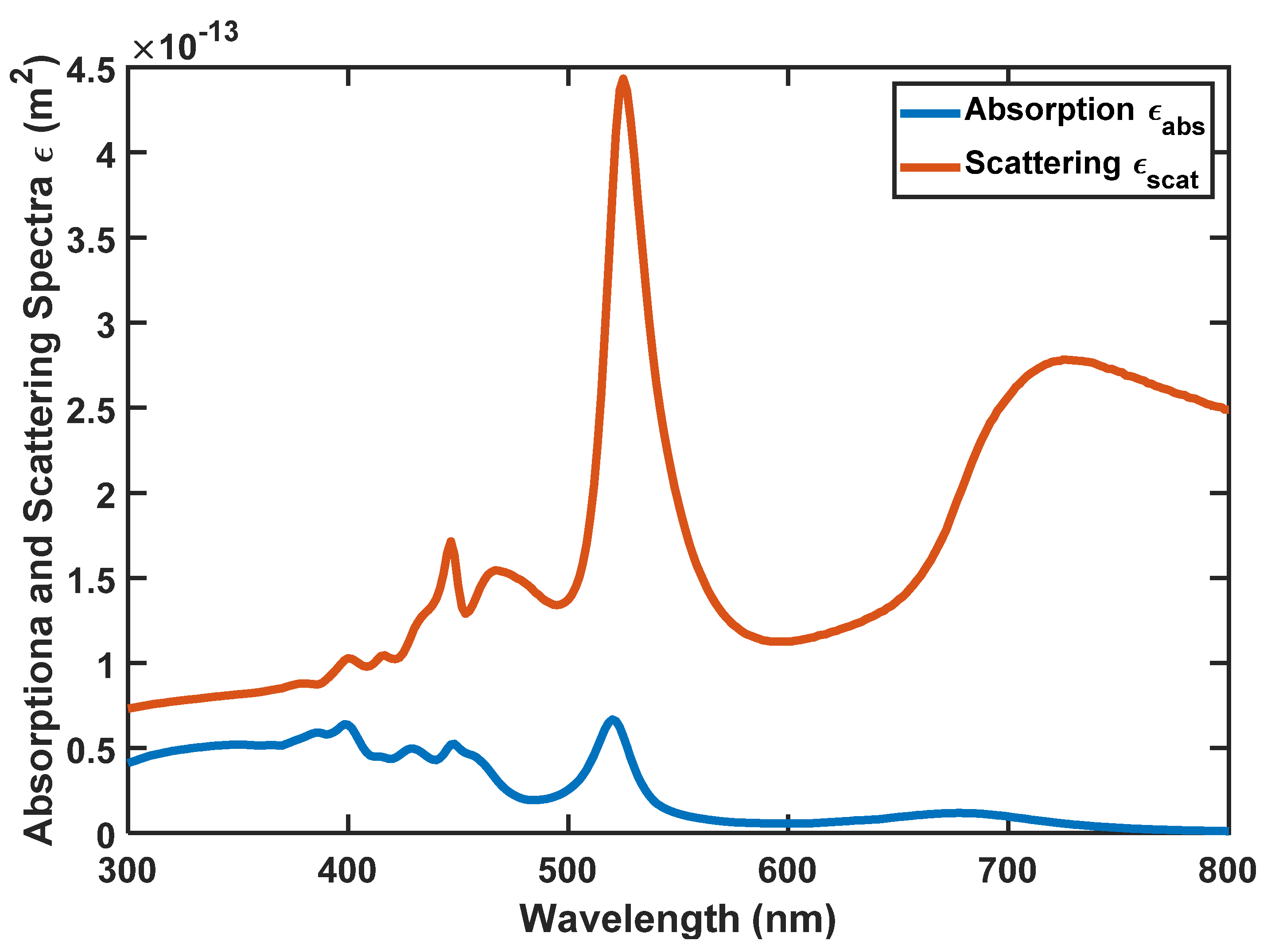
3. Results
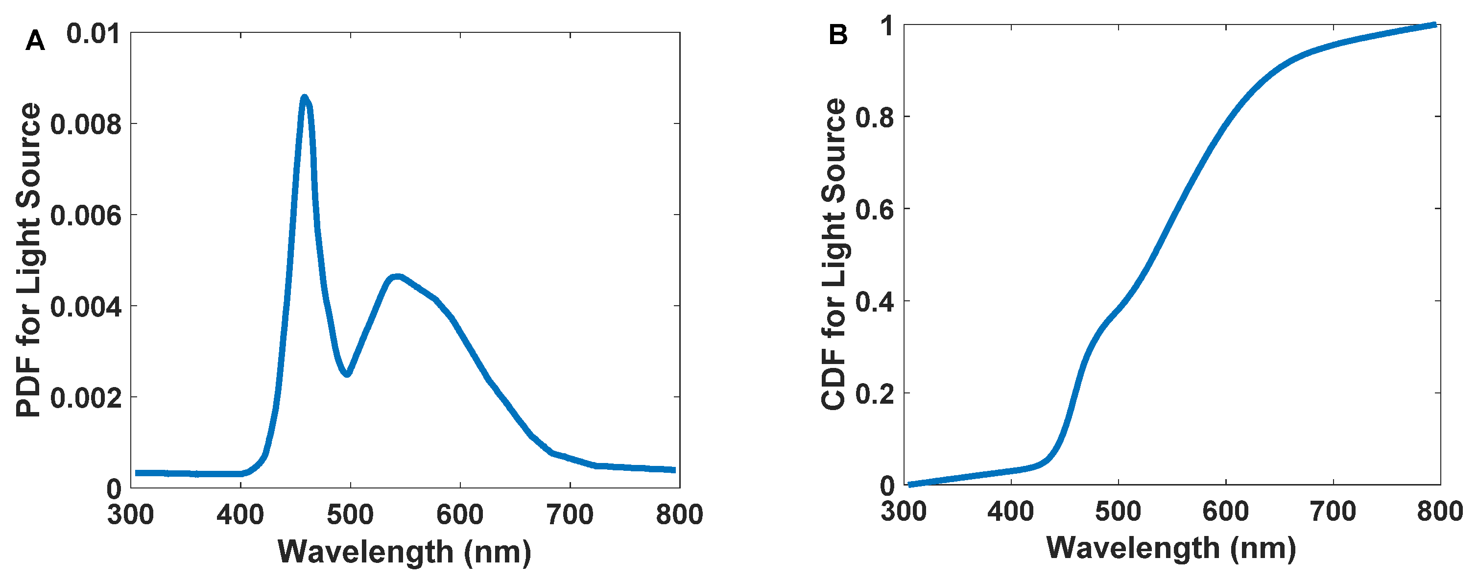
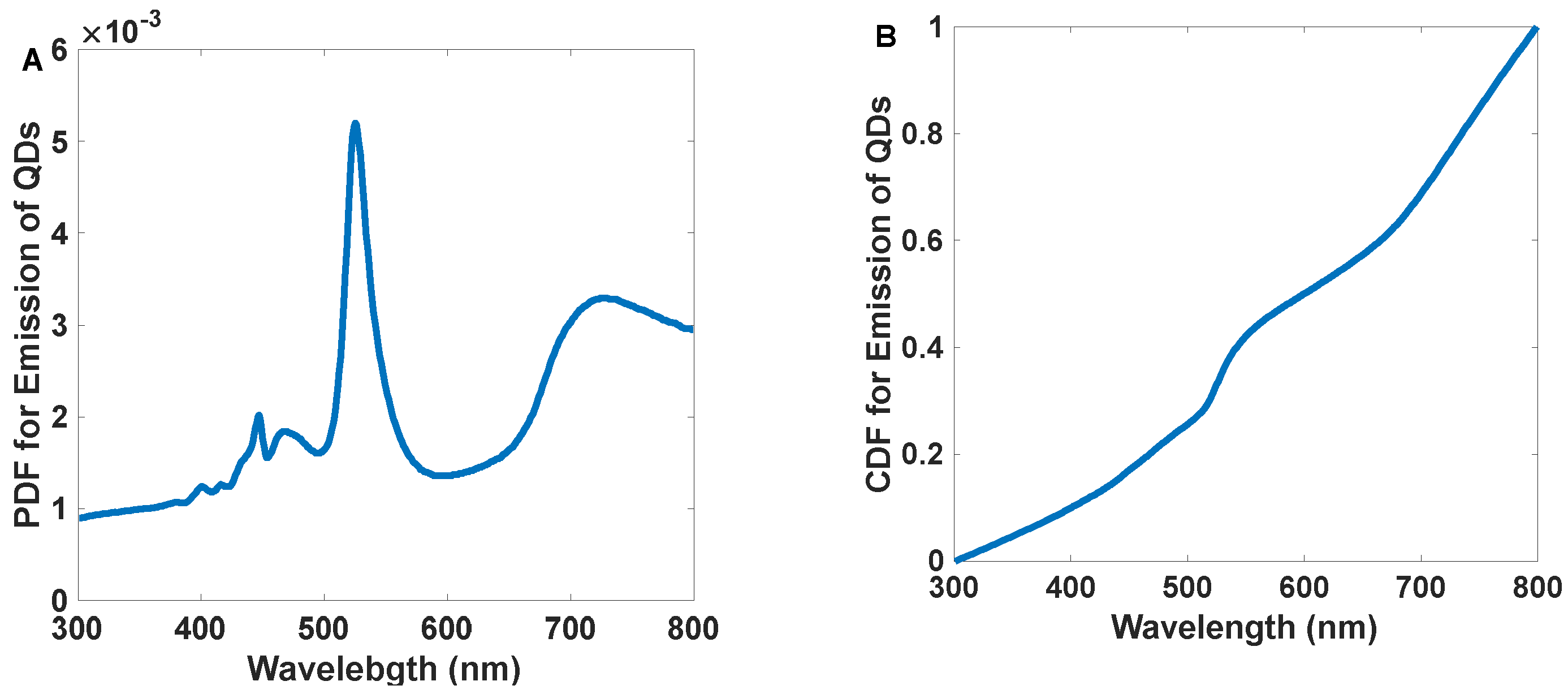
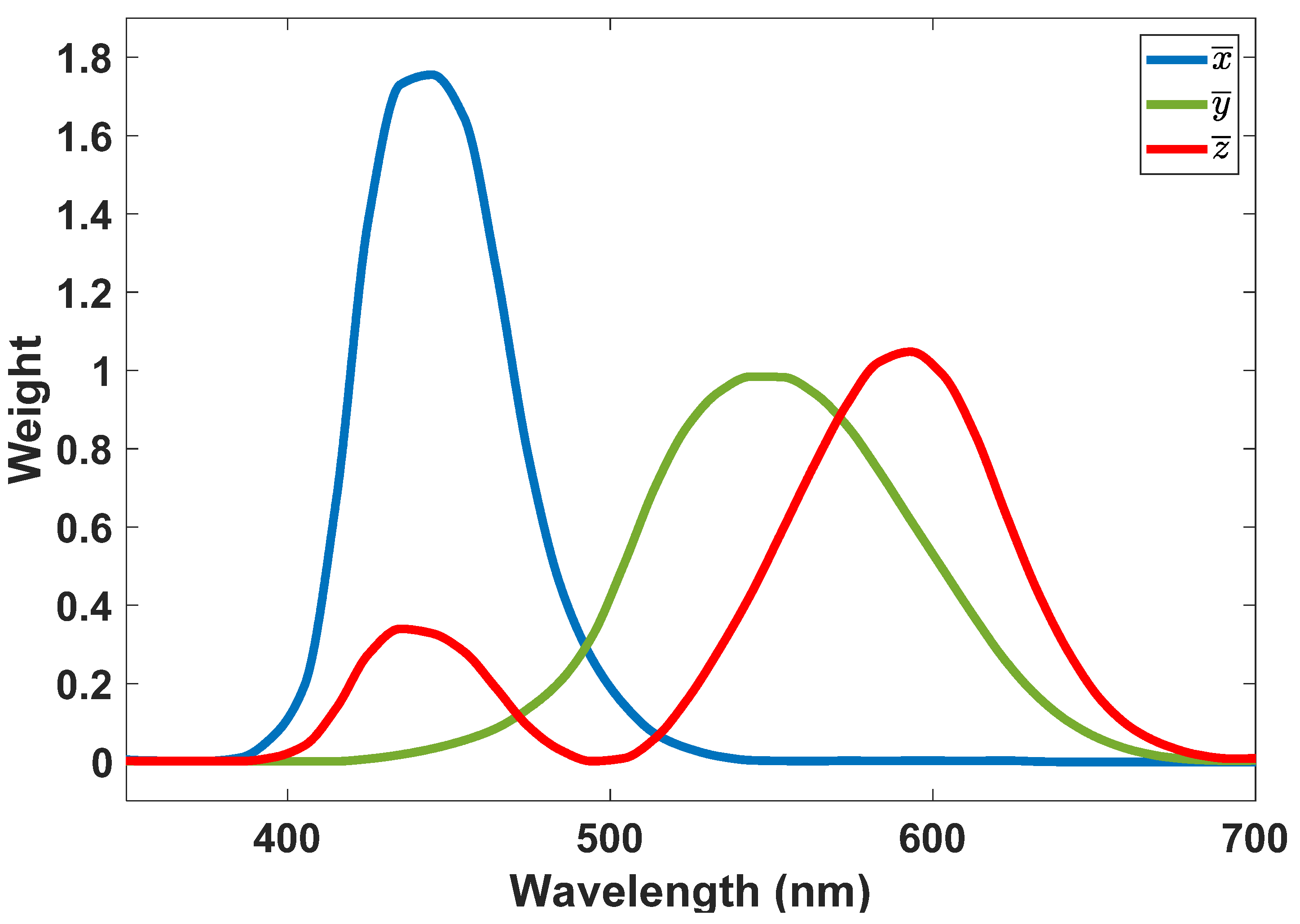
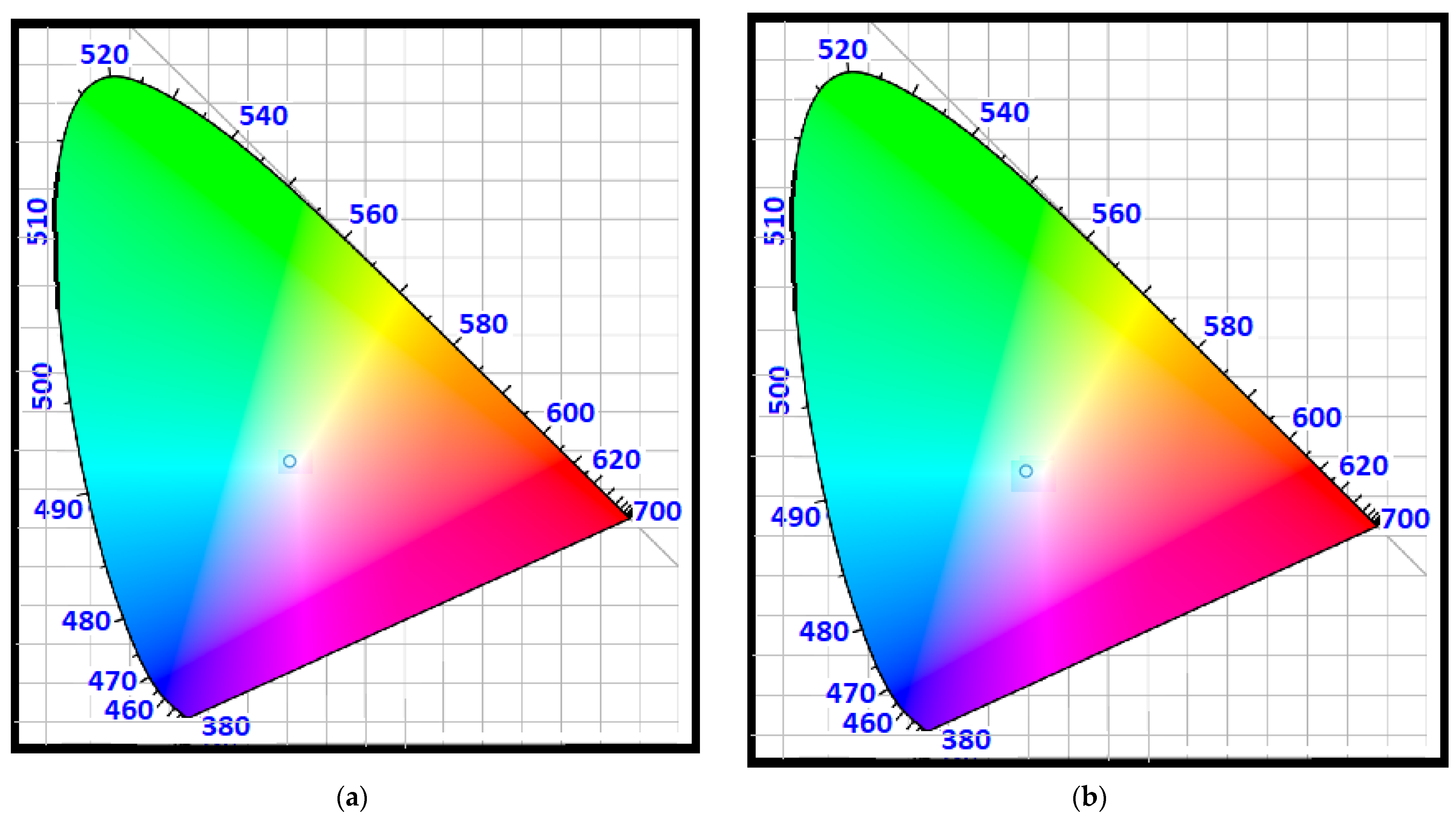
3.1. CIE Colorspace Comparison between LED Illumination and SiO2/Si QD Scattering
3.2. Results for Monte-Carlo Ray Tracing
4. Conclusions
Author Contributions
Funding
Data Availability Statement
Acknowledgments
Conflicts of Interest
References
- Dawy, Z.; Saad, W.; Ghosh, A.; Andrews, J.G.; Yaacoub, E. Toward Massive Machine Type Cellular Communications. IEEE Wirel. Commun. 2016, 24, 120–128. [Google Scholar] [CrossRef]
- Yahia, S.; Meraihi, Y.; Ramdane-Cherif, A.; Gabis, A.B.; Acheli, D.; Guan, H. A Survey of Channel Modeling Techniques for Visible Light Communications. J. Netw. Comput. Appl. 2021, 194, 103206. [Google Scholar] [CrossRef]
- Manousiadis, P.; Rajbhandari, S.; Mulyawan, R.; Vithanage, D.A.; Chun, H.; Faulkner, G.; O’Brien, D.C.; Turnbull, G.; Collins, S.; Samuel, I. Wide field-of-view fluorescent antenna for visible light communications beyond the étendue limit. Optica 2016, 3, 702–706. [Google Scholar] [CrossRef]
- Peyronel, T.; Quirk, K.J.; Wang, S.C.; Tiecke, T.G. Luminescent detector for free-space optical communication. Optica 2016, 3, 787. [Google Scholar] [CrossRef]
- Dong, Y.; Shi, M.; Yang, X.; Zeng, P.; Gong, J.; Zheng, S.; Zhang, M.; Liang, R.; Ou, Q.; Chi, N.; et al. Nanopatterned luminescent concentrators for visible light communications. Opt. Express 2017, 25, 21926. [Google Scholar] [CrossRef]
- Jenila, C.; Jeyachitra, R. Green indoor optical wireless communication systems: Pathway towards pervasive deployment. Digit. Commun. Netw. 2020, 7, 410–444. [Google Scholar] [CrossRef]
- Wu, C.; Lai, C.-F. A survey on improving the wireless communication with adaptive antenna selection by intelligent method. Comput. Commun. 2021, 181, 374–403. [Google Scholar] [CrossRef]
- Alsulami, O.; Hussein, A.T.; Alresheedi, M.T.; Elmirghani, J.M.H. Optical Wireless Communication Systems, A Survey. arXiv 2018, arXiv:1812.11544. [Google Scholar]
- Mukherjee, M. Wireless communication-moving from RF to optical. In Proceedings of the 10th INDIACom 2016 3rd International Conference on Computing for Sustainable Global Development, New Delhi, India, 16–18 March 2016; pp. 788–795. [Google Scholar]
- Merdan, F.A.B.; Thiagarajah, S.P.; Dambul, K. Non-line of sight visible light communications: A technical and application based survey. Optik 2022, 259, 168982. [Google Scholar] [CrossRef]
- Djordjevic, I.B.; Salehi, J.A.; Ghaffari, B.M.; Matinfar, M.D.; Kavehrad, M.; Hranilovic, S.; Lapidoth, A.; Moser, S.M.; Wigger, M.; Ding, H.; et al. Advanced Optical Wireless Communication Systems; Cambridge University Press: Cambridge, MA, USA, 2012; Volume 9780521197. [Google Scholar] [CrossRef]
- Grobe, L.; Paraskevopoulos, A.; Hilt, J.; Schulz, D.; Lassak, F.; Hartlieb, F.; Kottke, C.; Jungnickel, V.; Langer, K.-D. High-speed visible light communication systems. IEEE Commun. Mag. 2013, 51, 60–66. [Google Scholar] [CrossRef]
- Kedar, D.; Arnon, S. Urban optical wireless communication networks: The main challenges and possible solutions. IEEE Commun. Mag. 2004, 42, S2–S7. [Google Scholar] [CrossRef]
- Komine, T.; Nakagawa, M. Fundamental analysis for visible-light communication system using LED lights. IEEE Trans. Consum. Electron. 2004, 50, 100–107. [Google Scholar] [CrossRef]
- Lee, C.; Shen, C.; Cozzan, C.; Farrell, R.M.; Speck, J.S.; Nakamura, S.; Ooi, B.S.; DenBaars, S.P. Gigabit-per-second white light-based visible light communication using near-ultraviolet laser diode and red-, green-, and blue-emitting phosphors. Opt. Express 2017, 25, 17480–17487. [Google Scholar] [CrossRef]
- Eldeeb, H.B.; Uysal, M. Vehicle-to-Vehicle Visible Light Communication: How to select receiver locations for optimal performance? In Proceedings of the ELECO 2019—11th International Conference on Electrical and Electronics Engineering, Bursa, Turkey, 28–30 November 2019. [Google Scholar] [CrossRef]
- Ayyash, M.; Elgala, H.; Khreishah, A.; Jungnickel, V.; Little, T.; Shao, S.; Rahaim, M.; Schulz, D.; Hilt, J.; Freund, R. Coexistence of WiFi and LiFi toward 5G: Concepts, opportunities, and challenges. IEEE Commun. Mag. 2016, 54, 64–71. [Google Scholar] [CrossRef]
- Obrien, D.C.; Parry, G.; Stavrinou, P. Optical hotspots speed up wireless communication. Nat. Photonics 2007, 1, 245–247. [Google Scholar] [CrossRef]
- Zvanovec, S.; Chvojka, P.; Haigh, P.A.; Ghassemlooy, Z. Visible Light Communications towards 5G. Radioengineering 2015, 24, 1–9. [Google Scholar] [CrossRef]
- Daukantas, P. Optical Wireless Communications: The New “Hot Spots”? Opt. Photonics News 2014, 25, 34. [Google Scholar] [CrossRef]
- Nlom, S.M.; Ndjiongue, A.R.; Ouahada, K. Cascaded PLC-VLC Channel: An Indoor Measurements Campaign. IEEE Access 2018, 6, 25230–25239. [Google Scholar] [CrossRef]
- Cho, S.; Chen, G.; Coon, J.P.; Xiao, P. Challenges in Physical Layer Security for Visible Light Communication Systems. Network 2022, 2, 53–65. [Google Scholar] [CrossRef]
- Shaaban, K.; Shamim, M.H.M.; Abdur-Rouf, K. Visible light communication for intelligent transportation systems: A review of the latest technologies. J. Traffic Transp. Eng. 2021, 8, 483–492. [Google Scholar] [CrossRef]
- Karunatilaka, D.; Zafar, F.; Kalavally, V.; Parthiban, R. LED Based Indoor Visible Light Communications: State of the Art. IEEE Commun. Surv. Tutor. 2015, 17, 1649–1678. [Google Scholar] [CrossRef]
- Saadallah, N.R.; Fathi, M.M.; Arwa, R. The efficiency of Li-Fi (light –Fidelity) security and data transmission compared to Wi-Fi. Mater. Today Proc. 2021. [Google Scholar] [CrossRef]
- Ergul, O.; Dinc, E.; Akan, O.B. Communicate to illuminate: State-of-the-art and research challenges for visible light communications. Phys. Commun. 2015, 17, 72–85. [Google Scholar] [CrossRef]
- Smestad, G.; Ries, H.; Winston, R.; Yablonovitch, E. The thermodynamic limits of light concentrators. Sol. Energy Mater. 1990, 21, 99–111. [Google Scholar] [CrossRef]
- Ries, H. Thermodynamic limitations of the concentration of electromagnetic radiation. J. Opt. Soc. Am. 1982, 72, 380–385. [Google Scholar] [CrossRef]
- Welford, W.T.; Winston, R.; Sinclair, D.C. The Optics of Nonimaging Concentrators: Light and Solar Energy. Phys. Today 1980, 33, 56–57. [Google Scholar] [CrossRef]
- Li, H.; Wu, K.; Lim, J.; Song, H.-J.; Klimov, V.I. Doctor-blade deposition of quantum dots onto standard window glass for low-loss large-area luminescent solar concentrators. Nat. Energy 2016, 1, 16157. [Google Scholar] [CrossRef]
- Barbet, A.; Paul, A.; Gallinelli, T.; Balembois, F.; Blanchot, J.-P.; Forget, S.; Chénais, S.; Druon, F.; Georges, P. Light-emitting diode pumped luminescent concentrators: A new opportunity for low-cost solid-state lasers. Optica 2016, 3, 465–468. [Google Scholar] [CrossRef]
- Meinardi, F.; Ehrenberg, S.; Dhamo, L.; Carulli, F.; Mauri, M.; Bruni, F.; Simonutti, R.; Kortshagen, S.E.U.; Brovelli, F.M. Highly efficient luminescent solar concentrators based on earth-abundant indirect-bandgap silicon quantum dots. Nat. Photonics 2017, 11, 177–185. [Google Scholar] [CrossRef]
- Zhao, Y.; Meek, G.A.; Levine, B.G.; Lunt, R.R. Near-Infrared Harvesting Transparent Luminescent Solar Concentrators. Adv. Opt. Mater. 2014, 2, 606–611. [Google Scholar] [CrossRef]
- Shu, J.; Zhang, X.; Wang, P.; Chen, R.; Zhang, H.; Li, D.; Zhang, P.; Xu, J. Monte-Carlo simulations of optical efficiency in luminescent solar concentrators based on all-inorganic perovskite quantum dots. Phys. B Condens. Matter 2018, 548, 53–57. [Google Scholar] [CrossRef]
- Chamani, S.; Dehgani, R.; Rostami, A.; Mirtagioglu, H.; Mirtaheri, P. A Proposal for Optical Antenna in VLC Communication Receiver System. Photonics 2022, 9, 241. [Google Scholar] [CrossRef]
- Bessho, M.; Shimizu, K. Latest trends in LED lighting. Electron. Commun. Jpn. 2011, 95, 1–7. [Google Scholar] [CrossRef]
- Mirzaei, M.R.; Rostami, A.; Matloub, S.; Mirtaghizadeh, H. Ultra-high-efficiency luminescent solar concentrator using superimposed colloidal quantum dots. Opt. Quantum Electron. 2020, 52, 327. [Google Scholar] [CrossRef]
- Kalos, M.H.; Whitlock, P.A. Monte Carlo Methods; John Wiley & Sons: New York, NY, USA, 2009. [Google Scholar]
- Rubinstein, R.Y.; Kroese, D.P. Simulation and the Monte Carlo Method; John Wiley & Sons: New York, NY, USA, 1981. [Google Scholar]
- Wilton, S.R. Monte Carlo Ray-Tracing Simulation for Optimizing Luminescent Solar Concentrators. Master Thesis, The Pennsylvania State University, University Park, PA, USA, 2012. [Google Scholar]
- Hines, W.W.; Montgomery, D.C. Probability and Statistics in Engineering and Management Science; John Wiley & Sons: New York, NY, USA, 1980. [Google Scholar]
- Born, M.; Wolf, E. Principles of Optics; Elsevier: New York, NY, USA, 1959; 614p. [Google Scholar]
- Hecht, E. Optics, 4th ed; Addison-Wesley Publishing Company: San Francisco, CA, USA, 2001; p. 122. [Google Scholar]
- Hecht, E. Optics; Addison Wesley: San Francisco, CA, USA, 2002; Volume 10, p. 500. [Google Scholar]
- Bouguer, P. Essai d’optique, sur la Gradation de la Lumiere; Claude Jombert: Paris, France, 1729. [Google Scholar]
- Lambert, J.H. Photometria Sive de Mensura et Gradibus Luminis, Colorum et Umbrae. sumptibus vidvae E. Klett, typis CP Detleffsen, Germany, ISBN-10: 1279983108. 1760. Available online: https://www.amazon.com/Photometrie-Photometria-Mensura-Gradibus-Luminis/dp/1279983108 (accessed on 24 July 2022).
- Beer, A. Bestimmung der absorption des rothen lichts in farbigen flussigkeiten. Ann. Phys. 1852, 162, 78–88. [Google Scholar] [CrossRef]
- Ingle, J.D.J.; Crouch, S.R. The Beer-Lambert Law. In Spectrochemical Analysis; Prentice Hall: New Jersey, NJ, USA, 1988. [Google Scholar]
- Mayerhöfer, T.G.; Pahlow, S.; Popp, J. The Bouguer-Beer-Lambert Law: Shining Light on the Obscure. ChemPhysChem 2020, 21, 2028. [Google Scholar] [CrossRef]


| Parameter | Value or Type | Unit |
|---|---|---|
| FDTD simulation type | 3D | - |
| Simulation time | 800 | fs |
| Temperature | 300 | K |
| FDTD region x, y, z span | 3200 | nm |
| FDTD background material index | 1.46 | - |
| FDTD mesh type | Custom non-uniform | - |
| Mesh spacing | 1 | nm |
| Boundary condition in all directions | Perfectly Matched Layer (PML) | - |
| Source type | Planar TFSF source | - |
| Source x, y, z span | 1600 | nm |
| Source direction | Forward | - |
| Source amplitude | 1 | - |
| Source wavelength range | 300–800 | nm |
| Scattering calculation x, y, z span | 1800 | nm |
| Absorption calculation x, y, z span | 300 | nm |
| Shell material | Si | - |
| Core material | SiO2 | - |
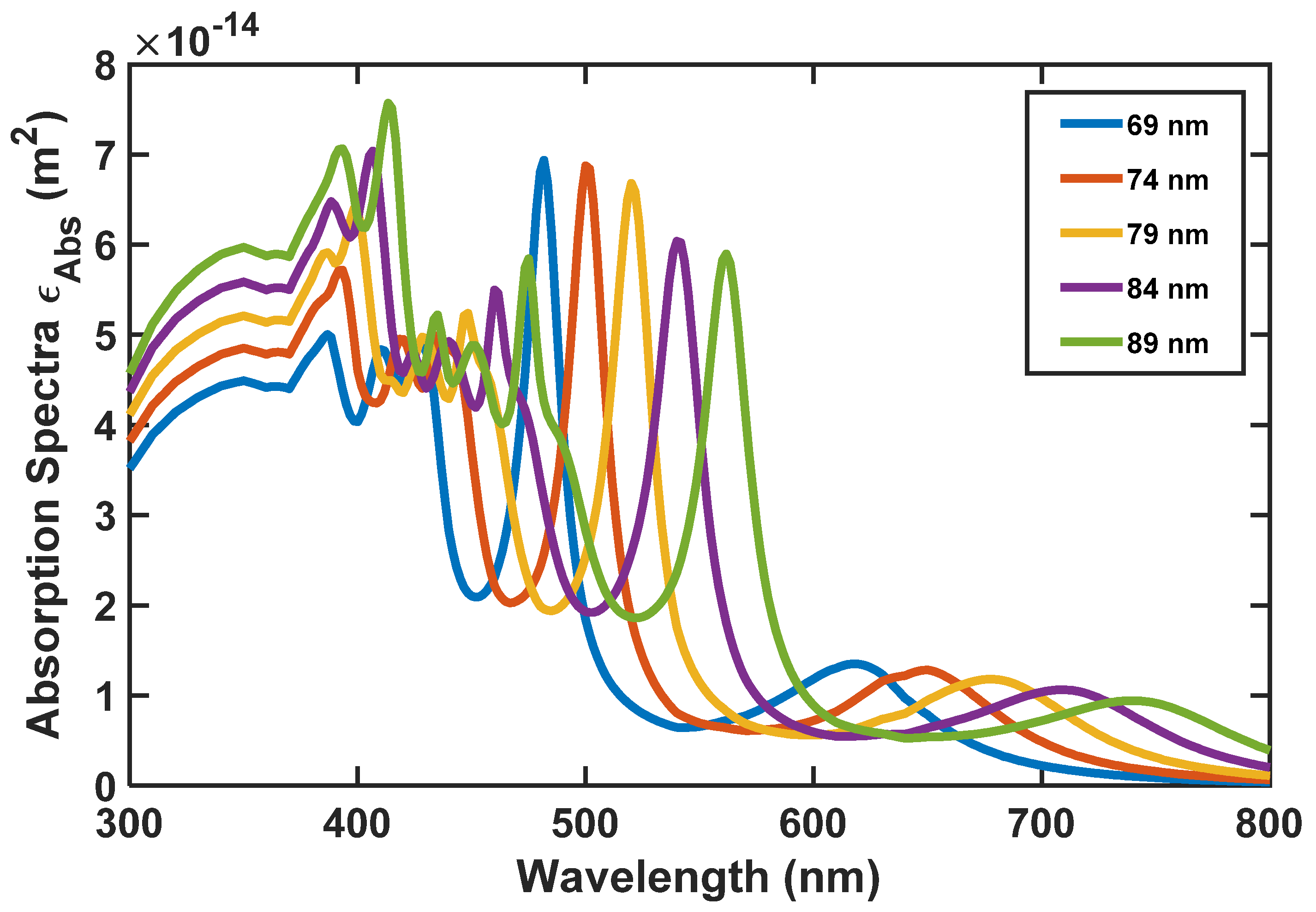
| Shell radius (R2) | Sweeping dimensions (85–95) | nm |
| Core radius (R1) | 6 | nm |
| Length (cm) | 2 | 4 | 6 | 8 | 10 | |
|---|---|---|---|---|---|---|
| QY = 0.3 | Optimal concentration (cm−3) | 3.88 × 10⁹ | 3.88 × 10⁸ | 3.88 × 10⁸ | 3.88 × 10⁸ | 3.88 × 10⁸ |
| Efficiency ηopt (%) | 1.0180 | 1.2034 | 1.5200 | 1.7832 | 1.9844 | |
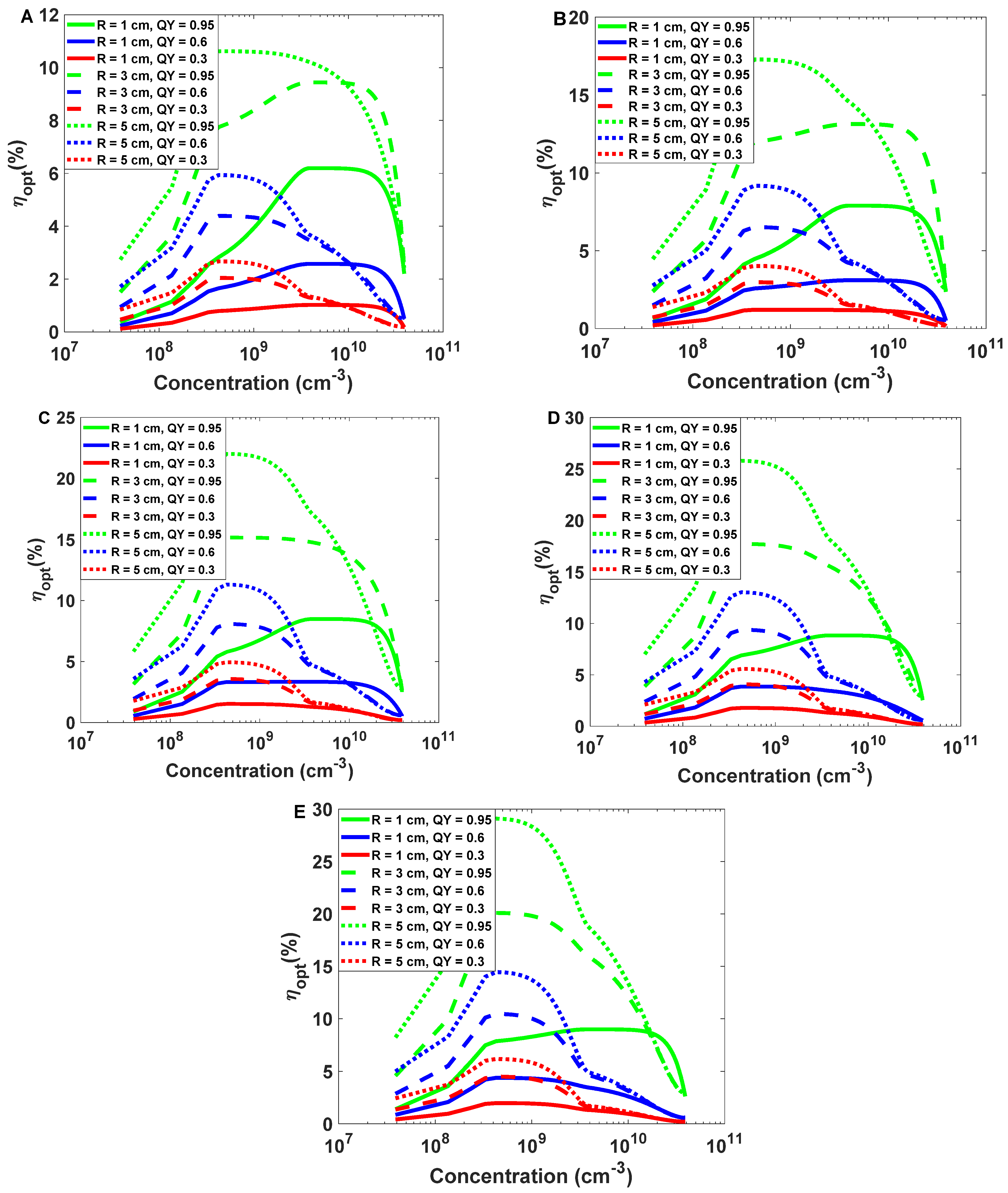
| QY = 0.6 | Optimal concentration (cm−3) | 3.88 × 10⁹ | 3.88 × 10⁹ | 3.88 × 10⁹ | 3.88 × 10⁸ | 3.88 × 10⁸ |
| Efficiency ηopt (%) | 2.5738 | 3.1016 | 3.3340 | 3.8666 | 4.3932 | |
| QY = 0.95 | Optimal concentration (cm−3) | 3.88 × 10⁹ | 3.88 × 10⁹ | 3.88 × 10⁹ | 3.88 × 10⁹ | 3.88 × 10⁹ |
| Efficiency ηopt (%) | 6.1952 | 7.8912 | 8.4874 | 8.8340 | 8.9946 |
| Length (cm) | 2 | 4 | 6 | 8 | 10 | |
|---|---|---|---|---|---|---|
| QY = 0.3 | Optimal concentration (cm−3) | 3.88 × 10⁸ | 3.88 × 10⁸ | 3.88 × 10⁸ | 3.88 × 10⁸ | 3.88 × 10⁸ |
| Efficiency ηopt (%) | 2.0432 | 2.9740 | 3.5698 | 4.0784 | 4.5104 | |
| QY = 0.6 | Optimal concentration (cm−3) | 3.88 × 10⁸ | 3.88 × 10⁸ | 3.88 × 10⁸ | 3.88 × 10⁸ | 3.88 × 10⁸ |
| Efficiency ηopt (%) | 4.3908 | 6.5162 | 8.0778 | 9.4004 | 10.4696 | |
| QY = 0.95 | Optimal concentration (cm−3) | 3.88 × 10⁹ | 3.88 × 10⁹ | 3.88 × 10⁸ | 3.88 × 10⁸ | 3.88 × 10⁸ |
| Efficiency ηopt (%) | 9.4390 | 13.1292 | 15.1644 | 17.7336 | 20.1008 |
| Length(cm) | 2 | 4 | 6 | 8 | 10 | |
|---|---|---|---|---|---|---|
| QY = 0.3 | Optimal concentration (cm−3) | 3.88 × 10⁸ | 3.88 × 10⁸ | 3.88 × 10⁸ | 3.88 × 10⁸ | 3.88 × 10⁸ |
| Efficiency ηopt (%) | 2.6706 | 4.0234 | 4.9420 | 5.5804 | 6.1712 | |
| QY = 0.6 | Optimal concentration (cm−3) | 3.88 × 10⁸ | 3.88 × 10⁸ | 3.88 × 10⁸ | 3.88 × 10⁸ | 3.88 × 10⁸ |
| Efficiency ηopt (%) | 5.9408 | 9.1848 | 11.3164 | 13.0406 | 14.4636 | |
| QY = 0.95 | Optimal concentration (m−3) | 3.88 × 10⁸ | 3.88 × 10⁸ | 3.88 × 10⁸ | 3.88 × 10⁸ | 3.88 × 10⁸ |
| Efficiency ηopt (%) | 10.6198 | 17.2854 | 22.0142 | 25.7964 | 29.0990 |
Publisher’s Note: MDPI stays neutral with regard to jurisdictional claims in published maps and institutional affiliations. |
© 2022 by the authors. Licensee MDPI, Basel, Switzerland. This article is an open access article distributed under the terms and conditions of the Creative Commons Attribution (CC BY) license (https://creativecommons.org/licenses/by/4.0/).
Share and Cite
Fakhri, D.; Alidoust, F.; Rostami, A.; Mirtaheri, P. A Monte-Carlo/FDTD Study of High-Efficiency Optical Antennas for LED-Based Visible Light Communication. Nanomaterials 2022, 12, 3594. https://doi.org/10.3390/nano12203594
Fakhri D, Alidoust F, Rostami A, Mirtaheri P. A Monte-Carlo/FDTD Study of High-Efficiency Optical Antennas for LED-Based Visible Light Communication. Nanomaterials. 2022; 12(20):3594. https://doi.org/10.3390/nano12203594
Chicago/Turabian StyleFakhri, Darya, Farid Alidoust, Ali Rostami, and Peyman Mirtaheri. 2022. "A Monte-Carlo/FDTD Study of High-Efficiency Optical Antennas for LED-Based Visible Light Communication" Nanomaterials 12, no. 20: 3594. https://doi.org/10.3390/nano12203594
APA StyleFakhri, D., Alidoust, F., Rostami, A., & Mirtaheri, P. (2022). A Monte-Carlo/FDTD Study of High-Efficiency Optical Antennas for LED-Based Visible Light Communication. Nanomaterials, 12(20), 3594. https://doi.org/10.3390/nano12203594