Article

Nanostructured MoS2 and WS2 Photoresponses under Gas Stimuli

1
Department of Nanotechnology and Advanced Materials, Graduate School of Applied and Natural Science, Selçuk University, Konya 42030, Turkey
2
Department of Nanoscience and Nanoengineering, Institute of Science and Technology, University of Necmettin Erbakan, Konya 42060, Turkey
3
Theoretical Physics Department, National Research Center, Cairo 12622, Egypt
4
Department of Physics, College of Sciences, Princess Nourah bint Abdulrahman University, P.O. Box 84428, Riyadh 11671, Saudi Arabia
5
Institute of Ceramics and Polymer Engineering, University of Miskolc, H-3515 Miskolc, Hungary
6
Department of Metallurgy and Material Engineering, Faculty of Engineering and Architecture, Necmettin Erbakan University, Konya 42060, Turkey
7
Department of Solar and Space Research, National Research Institute of Astronomy and Geophysics (NRIAG), Cairo 11421, Egypt
8
Department of Physics, Faculty of Science, Selçuk University, Konya 42075, Turkey
9
Department of Physics, Faculty of Science, Islamic University of Madinah, P.O. Box 170, AlMadinah Almonawara 42351, Saudi Arabia
10
Nanophotonics and Applications Laboratory, Physics Department, Faculty of Science, Beni-Suef University, Beni-Suef 62514, Egypt
*
Authors to whom correspondence should be addressed.
Nanomaterials 2022, 12(20), 3585; https://doi.org/10.3390/nano12203585
Submission received: 25 August 2022 / Revised: 27 September 2022 / Accepted: 30 September 2022 / Published: 13 October 2022
(This article belongs to the Special Issue Electrical, Optical, and Transport Properties of Semiconductors)

Abstract

:
This study was on the optoelectronic properties of multilayered two-dimensional MoS2 and WS2 materials on a silicon substrate using sputtering physical vapor deposition (PVD) and chemical vapor deposition (CVD) techniques. For the first time, we report ultraviolet (UV) photoresponses under air, CO2, and O2 environments at different flow rates. The electrical Hall effect measurement showed the existence of MoS2 (n-type)/Si (p-type) and WS2 (P-type)/Si (p-type) heterojunctions with a higher sheet carrier concentration of 5.50 × 105 cm−2 for WS2 thin film. The IV electrical results revealed that WS2 is more reactive than MoS2 film under different gas stimuli. WS2 film showed high stability under different bias voltages, even at zero bias voltage, due to the noticeably good carrier mobility of 29.8 × 102 cm2/V. WS2 film indicated a fast rise/decay time of 0.23/0.21 s under air while a faster response of 0.190/0.10 s under a CO2 environment was observed. Additionally, the external quantum efficiency of WS2 revealed a remarkable enhancement in the CO2 environment of 1.62 × 10⁸ compared to MoS2 film with 6.74 × 10⁶. According to our findings, the presence of CO2 on the surface of WS2 improves such optoelectronic properties as photocurrent gain, photoresponsivity, external quantum efficiency, and detectivity. These results indicate potential applications of WS2 as a photodetector under gas stimuli for future optoelectronic applications.

1. Introduction

Photodetectors have a wide range of applications in the fields of biomedical sensing, environmental monitoring, optical communications, and space exploration. It is well known that photodetector responsivity is mainly dependent on the device material, structure, and operating conditions in terms of bias voltage, temperature, and wavelength of the incident radiation. It thus becomes crucial to have a thorough understanding of the effects of these parameters for designing and fabricating an optimal photodetector [1]. Nowadays, space has become a new and rich field, as well as a preferential development sector, which is rapidly contributing to countries’ financial welfare and progress. Space technologies play a key role in accelerating countries’ development processes and increasing societies’ quality of life and security. Aerospace and space applications require the development of sensors that are operated in several different environments. Future aeronautical systems will need to be more capable, perform better, and be safer, all of which will require less maintenance. Space sensors and detector application areas include optical, photodetector, leak detection, high temperature, emissions monitoring, fire detection, environmental monitoring, and radiation detection. Each of these detectors is the subject of effort throughout NASA to improve safety and decrease the cost of space travel, significantly reduce the number of emissions produced by aeronautic engines, and improve the safety of commercial airline travel. Testing the performance of the photodetectors under different gas environments is essential to understand their performances under various gas stimuli. For instance, CO2 is considered one of the primary gases in the space environment and the greenhouse gases in the Earth’s atmosphere [2,3,4]. The Martian atmosphere is primarily composed of 96% CO2 with a balance of nitrogen, argon, and trace species [5]. There is a highly significant need for testing the performance of optoelectronic devices under different gas environments, such as CO2, for space and commercial applications.
The exotic physical characteristics of 2D transition metal dichalcogenides (TMDC), such as their non-zero bandgap and layer-dependent second-order optical nonlinearity, are garnering a lot of interest. The chemical formula MX2 refers to a class of inorganic 2D layered materials where M is a transition metal (typically M = Mo, W, Ti, V, Ta, Hf, and Pt) and X is a group of VI chalcogen atom (typically X = S, Se, and Te). The advantages of both materials are that they can be combined by forming heterojunctions with silicon using 2D layered materials. By being completely compatible with conventional integrated circuit fabrication techniques, it streamlines the manufacturing process; because they have a bandgap of 2 eV in monolayer form. MoS2 and WS2 are the most studied materials in the TMDC family [6]. WS2 is more desirable for optical, electrical, and optoelectronic applications due to its novel properties, including high thermal stability and a wide range of operating temperatures [7], layer-dependent tunable bandgap (1.4–2.1 eV) [8], broad UV-visible absorption spectrum [9], and tunable photoluminescence (PL) effect [10,11,12].
Graphene, WS2, MoS2, and other materials can be produced into 2D sheets using “top-down” techniques like exfoliation methods. Among these, micromechanical exfoliation [13], sonication-assisted liquid exfoliation [14,15,16], shear exfoliation [17,18], and chemical exfoliation [19,20] have been studied and suggested in the literature. However, they have several disadvantages, such as low quality and small-scale production, many flaws, and a short-range during micromechanical exfoliation [21]. Additionally, transferring the exfoliated layer to a new substrate is required, which makes scaling up and large-scale production more difficult [22]. For this reason, chemical vapor deposition (CVD) with a bottom-up process is preferred during the synthesis of MoS2 [23,24]. MoO3 substrate is maintained in the downstream gas flow during growth [25,26,27]. Thin-film properties like homogeneity and grain size are strongly dependent on MoO3 substrate properties. Nowadays, the creation of wafer-scale and homogeneous 2D materials has attracted great attention due to the advancement of the following generation of optoelectronic applications and quantum computers. Atomic layer deposition (ALD) [22,28], pulsed laser deposition (PLD) [29,30], thermal evaporation [31,32,33], and magnetron sputtering systems [34,35,36] are commonly used for the preparation of MoO3 substrates. However, magnetron sputtering is the most preferred, since its low cost and ease of control are suitable for large-scale commercial manufacturing. MoO3 is sulfurized within a two or three-zone quartz tube under an Ar inert atmosphere via sublimation of sulfur powders. Similar processes are used with WO3 to grow WS2 TMDC.
WS2 and MoS2 are two TMDC thin films that have tunable optical bandgaps, making them promising for photodetection applications. A suitable structure may be sensitive to an incident light involving a photocurrent whose intensity is compared to the current under darkness (dark current) [37]. Photoconduction and photogate are two major effects that contribute to photocurrent [38]. The process of photoconduction happens when free charge carriers are absorbed by light with photon energy greater than the MoS2 (or WS2) bandgap. The highest photo responsiveness occurs when all photons are absorbed and each input photon produces one electron and one hole. This indicates that the primary photoresponse mechanism in MoS2 (or WS2) phototransistors is a photogate, in which light absorption introduced a change in the trapped charges density. When photogate occurs in the MoS2 (or WS2) thin film, the threshold voltage VTH, the gate voltage separating the high-current (ON) and low-current (OFF) regimes, shifts as a result of trapped charges causing a change in the effective gate voltage, which introduces a great increase in current [39].
Gas adsorption can affect the Fermi-level energy of MoS2 [40]; therefore, several investigations on 2D TMDC-based photodetectors and gas sensors have been conducted [41]. The effect of O2, N2, and Ar on the optoelectronic rGO performance was studied [42]. As with n-type rGO, oxidizing gases such as O2, CO2, and N2 pull electron clouds from the n-type semiconductor sheets, resulting in a drop in charge carriers and an increase in resistance [42,43]. Different compounds have also been tested, such as the effect of the atmosphere on the device performance of perovskite solar cells during operation. Indeed, Guo et al. [44] investigated the degradation mechanisms of perovskite solar cells operated under a vacuum and a nitrogen atmosphere.
According to our investigations, there is no complete work related to the study of the effect of CO2 gas adsorptions on MoS2 and WS2 by examining and comparing photodetection parameters. To fabricate MoS2 and WS2-based optoelectronic photodetector sensors, PVD layers of molybdenum and tungsten oxide were deposited on silicon substrates, then sulfurization occurred in a CVD chamber. The effect of different gas adsorptions, such as air, O2, and CO2, on MoS2 and WS2 thin films, were investigated in this work. In addition, their optoelectronic performance under UV illumination is discussed in detail.

2. Materials and Fabrication Methods

2.1. Fabrication of Thin Films

The fabrication process of MoS2 and WS2 thin films is similar to the previously reported studies [45,46]. The advantage of this process is to increase film homogeneity and scalability. This method also demands that there are no small discounted triangular-like shapes of MoS2 or WS2, as known for the CVD deposition process of 2D materials. MoS2 and WS2 thin films were prepared on a p-type silicon substrate first by using a PVD system, which included an RF magnetron sputtering system followed by a CVD process. Substrates of Si were cleaned in a series of steps, firstly a 5 min dip in an NH4OH-H2O2 solution watered down with pure water at 75 °C. Then, they were put in a 5% HF solution for 5 s, after which they were washed in pure water and dried with N2. The Si substrates were put into the RF magnetron sputtering system right away. To activate the Si surface, a 100 W Ar-plasma source was opened for 10 min at room temperature. Targets made of tungsten and molybdenum were used as the primary sources, with Ar plasma serving as the carrier gas and O2 as the reactive gas. The substrate temperature was kept under control at 400 °C for more than 30 min, increasing by 100 °C/30 min. We maintained constant O2 and Ar flow rates. The films were deposited at 5E-3 Torr and 137 W using 30 s sputtering times. Before being moved to the two-zone CVD quartz chamber for the sulfurization process, the system was naturally cooled to room temperature. In the center of the CVD furnace, the temperature of the Mo-O and W-O thin films as they were being deposited was elevated to 650–750 °C. A 100 sccm Ar source was used with a ceramic boot that contained 0.5 g sulfur powder. An external heating belt was used to evaporate the sulfur for 25 min at a distance of 50 cm from the substrate. The system then cooled until it reached RT while receiving an Ar flow rate of 100 sccm.

2.2. Characterization Techniques

Field-emission scanning electron microscopy (FE-SEM; Zeiss Gemini 500, Cambridge, UK) was used to record the surface morphology. The topography and line profile spectrum were examined using atomic force microscopy (AFM, Park, Santa Clara, CA, USA) Park XE7 system via noncontact mode through a 1 × 1 µm scanning area and a tip scan speed of 1 Hz. XEI 4.3.4 2016 data processing and analysis software (Park, Santa Clara, CA, USA) were used to measure the roughness values. In addition, confocal Raman microscopy was utilized to introduce thin film optical images. X-ray photoelectron spectroscopy (XPS) measurements were investigated based on the Thermo Scientific K-alpha XPS system (Thermo Scientific™, Waltham, MA, USA) using an Al Kα source and a spot size of 400 µm. Photoluminescence (PL) and Raman vibrational modes were performed using Renishaw inVia confocal Raman microscope (Renishaw, New Mills, UK) with a laser beam of a wavelength value of 532 nm. SWIN Hall8800 Hall Effect measurement system is employed to measure the carrier’s concentration and mobility. The electrical I-V and optoelectronics measurements were carried out using Tektronix Keithley 2400 Sourcemeter (20 mV and 10 nA sensitive, Tektronix, Beaverton, OR, USA) through a four-probe system and KickStart Keithley software (Tektronix, Beaverton, OR, USA) for data acquisitions. A 365 nm ultraviolet (UV, Konya, Turkey) light lamp was used for illumination. The same calculations and measurements can be reported under different gas (such as CO2) and temperature environments by using a stain steel vacuum chamber with a quartz window, as shown in Scheme 1. The system has a quartz window that can be used to transmit light into the sample easily under temperature or gas environments. The temperature can be controlled with a Lake Shore Model 335 Cryogenic Temperature Controller (Woburn, MA, USA). These measurements were repeated under high-purity gases of O2, CO2, and N2 to study the stimuli effects. Here, the role of N2 was just to clean/stabilize the environment around the photodetector sample. Since we were using different gases (CO2 and O2), cleaning the environment around the sample with a vacuum and inert gas (N2) was necessary. The gases are controlled with the Alicat Scientific Mass flow meter MC model. All the measurements were recorded and captured from the computer, and after that, the analyses were carried out.

3. Results and Discussion

3.1. Raman and PL Spectra

The Raman spectra of 2D materials show characteristics of two main peaks with E 2 g 1 and A 1 g   modes. According to the literature, Mo–S atoms vibrate in the plane at E 2 g 1 = 382.01 cm−1 while S atoms oscillate perpendicular to the plane at A 1 g = 407 cm−1, as shown in Figure 1a [23,24,47]. Concerning WS2, E 2 g 1 and A 1 g modes, the peaks are located at 354.08 and 420.09 cm−1, respectively. The differences between E 2 g 1 and A 1 g for MoS2 and WS2 are 23.76 and 66.01 cm−1, respectively. These results show the existence of multilayered MoS2 and WS2 structures of a few nanometers in size, as has been reported before [24,45,48].
From the measurements of photoluminescence (PL), it can be seen that the thin films introduced a direct and indirect electronic band transition. MoS2′s optical properties are greatly influenced by the number of layers. The energies of direct excitonic transitions have a substantial PL effect in monolayer MoS2, but this effect is reduced due to the layer’s number increasing and completely disappearing in bulk MoS2. The PL spectra of MoS2 are observed at 610 and 624 nm (Figure 2a). These peaks are related to direct excitonic transitions at the Brillouin zone of the K point and represent the A and B excitation of MoS2 [49]. Furthermore, photogenerated electron-hole pair recombination is attributed to the prominent peak at 682 nm, while the valence band separated as the MoS2s high spin-orbit coupling is attributed to the lesser peak at 624 nm [50]. Nevertheless, the trion exhibits localized quasiparticles with negative (two electrons with one hole) and positive (two holes with one electron) charges as PL peaks at 682 nm. According to the report, the monolayer introduced a strong peak at 615 nm (2.02 eV) that was associated with the A exciton resonance. It is believed that at the K point, the direct exciton transition between the maximum of the valence band and the minimum of the conduction band (CBM) is what causes the PL in the monolayer [51]. However, the bilayer and trilayer PL spectra show wider and lower energy emissions than those of the indirect exciton, in which the VBM is still at the K point but the CBM is located between the K point and the peaks [52]. For WS2, two peaks at 612 and 700 nm are observed (Figure 2b).

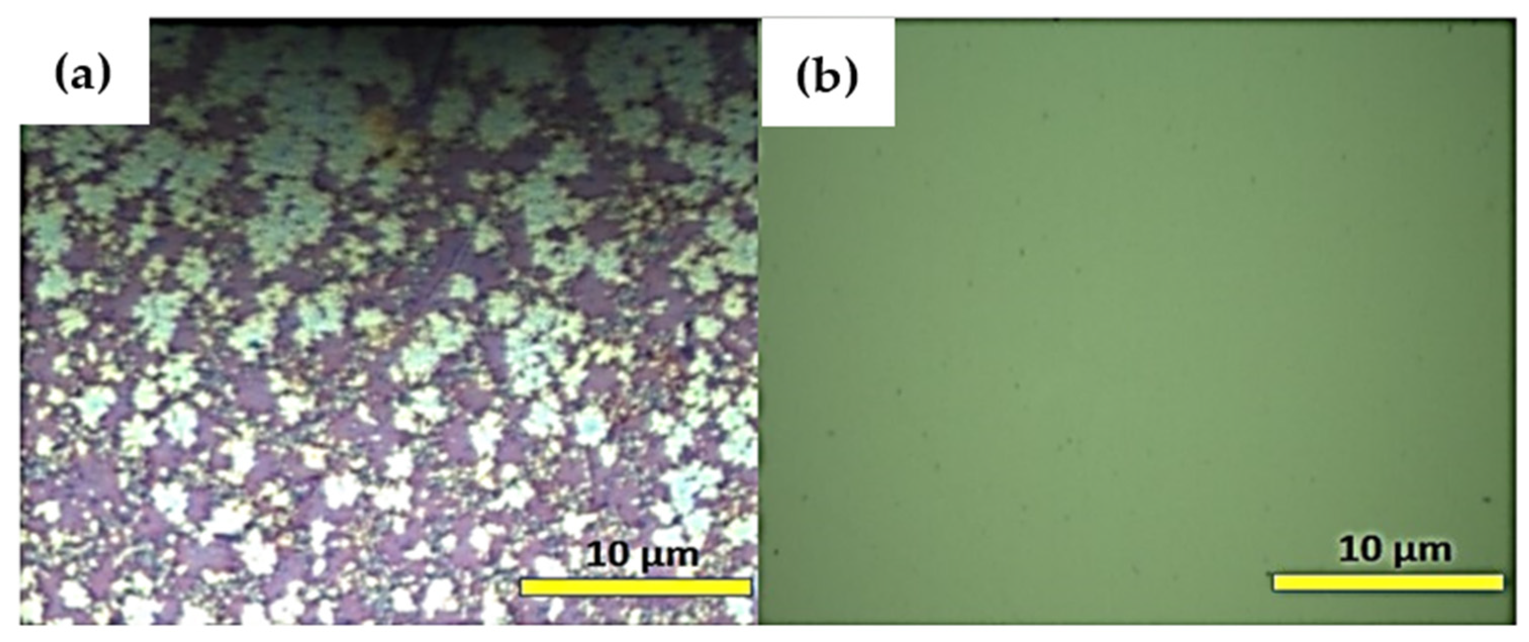
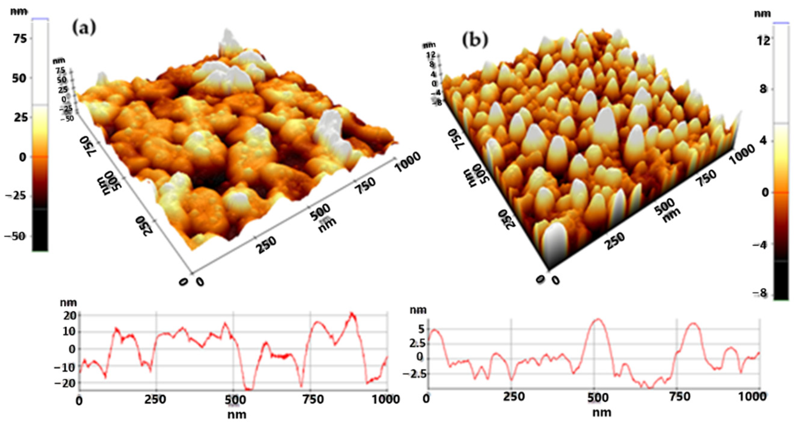
3.2. Surface Morphology and Topography

Large-scale MoS2 thin films have been previously worked on by combining CVD and sputtering techniques [53]. Optical microscopy was used to capture the MoS2 and WS2 surfaces, as seen in Figure 3a,b, respectively. At a macroscopic scale, the texture of WS2 is more homogeneous than that of MoS2. The structural domains of WS2 are smaller than those of MoS2 (see Figure 3b).
The high-resolution FE-SEM images show quite a homogeneous distribution of a few nanometers that contain nanocrystals for both materials (Figure 4). However, the particles of MoS2 are relatively smaller than those of WS2. In both materials, particles are well interconnected to each other. Nevertheless, the WS2 surface contains more cracks than MoS2, which is important for surface gas adsorption and light-trapping applications [54].
The topography of the prepared samples was measured by AFM using a noncontact mode of a 1 × 1 μm area. Figure 5a,b show the 3D AFM topography and the horizontal line profile of MoS2 and WS2 samples, respectively. The roughness values of MoS2 and WS2 are 10.689 and 2.761 nm, respectively, as depicted in Table 1. The optical microscopy analysis also shows that MoS2 has higher surface roughness than WS2 film.

3.3. XPS and Oxidation States

The WS2 and MoS2 chemical states were examined through XPS survey analyses. The binding energies of S 2p, Mo 3d, C 1s, and O 1s are introduced by the characteristic peaks at 161 eV, 230 eV, 285 eV, and 532 eV, respectively [55], as shown in Figure 6a. The XPS survey analyses of WS2 showed distinct signals of C, O, S, and W elements, as seen in Figure 6b. The W 4d3/2 spin-orbital splitting photoelectrons in the WS2 nanostructures are reconsidering the W peak at 283.0 eV [56]. In addition, the W 4d3/2 peak binding energy is higher than the W atom, which confirms the presence of W with a valence of +4 [57].

3.4. Sheet Resistance and Hall Coefficient

Electrical characterization of the prepared MoS2 and WS2 thin films was carried out using a Hall-effect measurement system (Table 1). Table 2 displays the Rs (sheet resistance), Rho (resistivity), VH (Hall voltage), RH (Hall coefficient), Ns/Ps (sheet carrier concentration), N/P (carrier concentration), and Mob (mobility). When VH has a positive (negative) value, the majority of the sample’s carriers are of the p (n) type. All measurements were performed with a 7210 G magnetic field and a temperature of 300 K. We observed an enhancement in the electrical mobility properties of the WS2 compared to the MoS2 thin film. The MoS2 film shows an n-type and WS2 is p-type semiconductor behavior [58]. Based on these investigations of Hall-effect measurements, it was observed that our devices are MoS2 (n-type)/Si (p-type) and WS2 (P-type)/Si (p-type) heterojunctions. The highest carrier concentration, as well as carrier mobility for p-p heterostructure, was higher than that of the p-n device, suggesting better performance for the WS2/Si device.

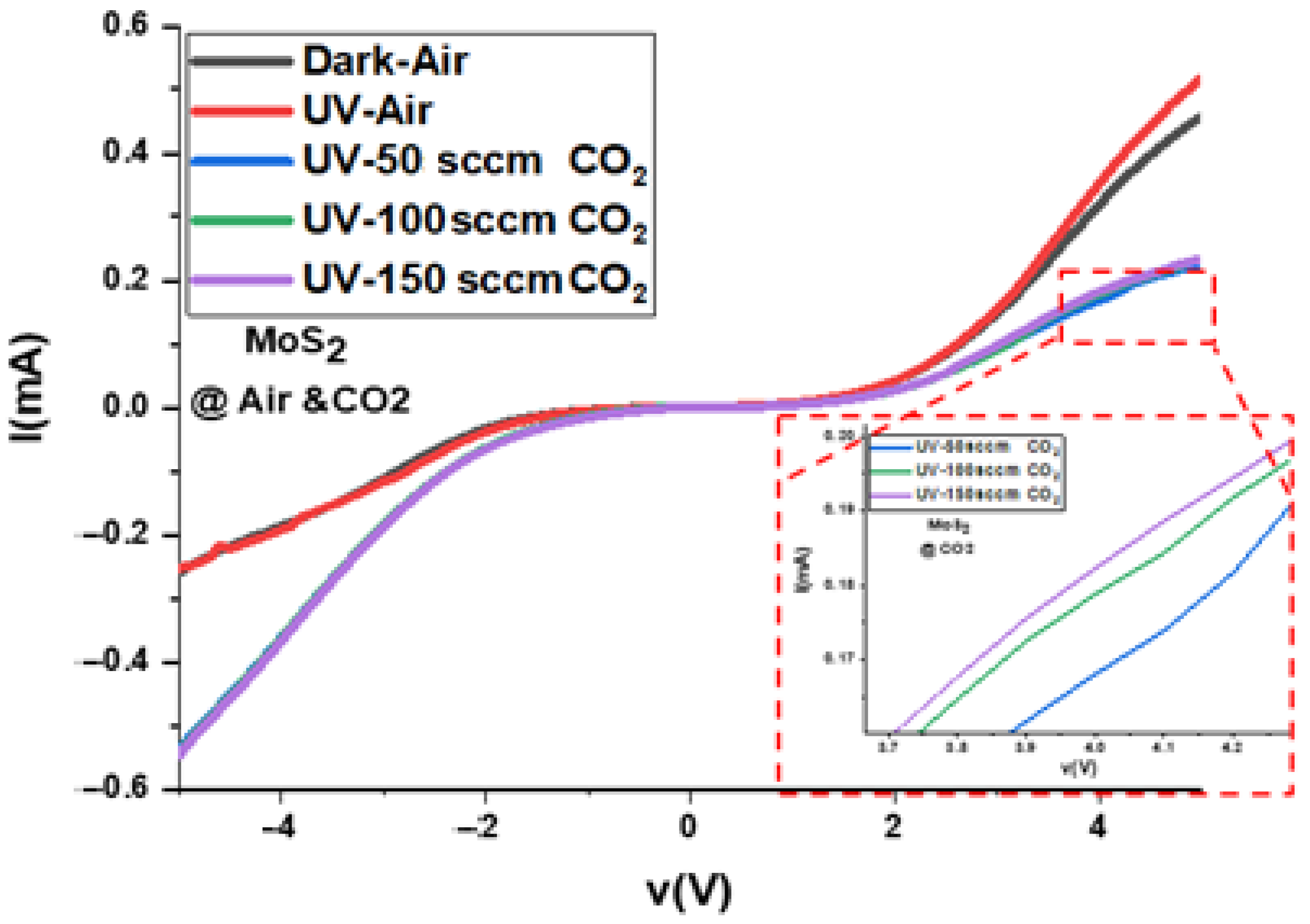
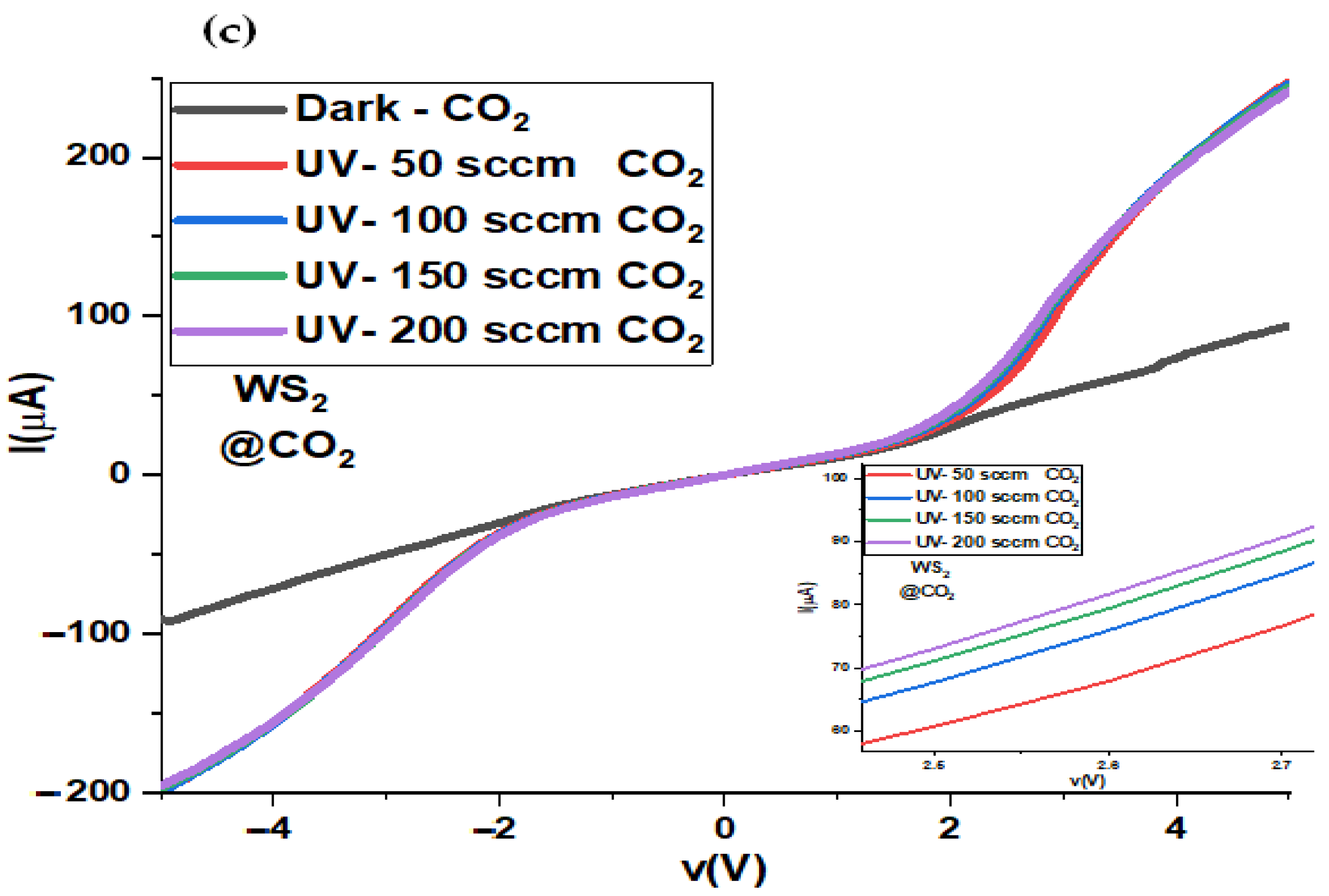
3.5. Electric and Optoelectronic Characteristics

The current-voltage (I-V) electrical characteristics of MoS2 and WS2 were examined under air conditions in absence of light and 365 nm ultraviolet illuminations. The device size was 1 × 1 cm2, and we used silver paste for making the contacts with a width of 3 mm and a length of 1 cm. The vertical electron transfer (electrical and optoelectronic) multilayered MoS2/Si and WS2/Si heterostructures were investigated and active edge sites with high density [59] are shown in Figure 7. As mentioned above, a high resistance layer like SiO2 [60], which increased the ideal structure vertical conductivity, is not presented in the currently optimized photodetector.
MoS2: The idea of measuring the optoelectronic performance of devices under different gas stimuli, such as CO2, has received much interest for many environmental and industrial applications. The behavior of optoelectronic photodetectors under a toxic gas environment such as CO2 may predict the general performance of devices. Figure 8 shows the I-V curve of MoS2 in dark and UV conditions of 365 nm under air and CO2 gas stimuli. Under dark and illumination conditions, nonlinear I-V curves were observed, showing the generation of an excellent double-Schottky contact between the silver (Ag) electrode and film surfaces, as predicted before [61]. The observed photocurrent is small compared to the dark current in the air. Under CO2 gas flow, the photocurrent is lower than the one under air in both positive and negative parts. This result shows the n-type behavior of MoS2 under CO2. CO2 gas can capture the electrons from the conduction band of the n-type MoS2 surface, which consequently can decrease the current. Since CO2 does not absorb light at 365 nm, the reduction in photocurrent is related to its oxidizing properties that act on the MoS2 surface. Similar behavior has been predicted before for different n-type semiconductor materials [42,43]. Moreover, by increasing the CO2 gas flow from 50 to 150 sccm, a further but less pronounced photocurrent decrease is observed, supporting the effect of oxidation.
To check the behavior of the MoS2 photodetector with time, we measured the change in the photocurrent in the air under dark and light illumination conditions, as shown in Figure 9a. The measurements are carried out at different bias voltages from 0 to 5 V. The MoS2 in air did not show a good response at zero bias, but the response started to appear from 0.5 V. With increased applied bias, the sensor performance becomes dominated and more stable and produces higher photocurrent. Figure 9b shows the on–off time-resolved photoresponse of MoS2 thin film under a different bias voltage of 0–5 V. The measurements were recorded every 30 s and started with dark mode followed by the UV-on illumination mode. The dynamic curve of the MoS2 at zero bias did not show a good signal, confirming that it is not a self-bias photodetector. However, with a small bias of 0.5 V, a clear signal gets released. We see that at higher applied biases, the device is working more efficiently, as expected.
To check the photocurrent time and the on–off behavior of the MoS2 photodetector in air and CO2, we chose a bias of 5 V. Figure 10a,b show the photocurrent behavior with time and on–off time-resolved photoresponse of MoS2 thin film under the absence of light and UV illumination conditions in both air and 50 sccm CO2 environments at a bias voltage of 5 V. The behavior of the photocurrent in both cases (air and CO2) is more or less the same. Therefore, in the case of CO2, we see that the dark current is decaying with time but the photocurrent is increasing, similar to the case of air. However, the decreasing and increasing rate of the current for the case of CO2 stimuli is less than in the case of air, confirming the better stability of the MoS2 photodetector in CO2 than in an air environment. The position of the CO2 curve is lower than that of the air, due to the capturing mechanism of the CO2 of electrons and subsequently increasing the resistance. On the other hand, for the on–off curve in Figure 10b, the MoS2 photodetector in CO2 long-term stability with time is better than in the case of air. In both cases, the response and recovery time are relatively long.
On the other hand, for WS2, we observed a better response than MoS2 thin film. We measured the electrical IV properties of WS2 thin film under dark and UV illuminations in air, O2, and CO2 environments, as in Figure 11. The IV curve in air is illustrated in Figure 11a. We observed a better response under light illumination in both positive and negative parts than in the case of MoS2 thin film. However, for the IV of MoS2 above, only a small improvement in the positive current was shown, but there were no changes in the negative section. This indicated that WS2 is more interesting for optoelectronic applications, so we tested WS2 film under O2 and CO2 environments. In the case of 100 sccm O2 stimuli, its photocurrent is decreasing for both dark and UV cases, as represented in Figure 11b. This shows that the Fermi level’s position has a substantial effect on O2 and CO2 molecule adsorption and desorption at the surface. Charge transfer is expected to attract electrons from the p-type WS2 layer because CO2 is an electronegative molecule [62].
Normally, O2 and CO2 are oxidizing gases due to their high affinity for electrons and high electronegativity. However, in the case of CO2 molecules, the electronegativity is stronger than in the O2 case. We observed an increase in the photocurrent under the CO2 environment in Figure 11c. The photocurrent is increased with increasing the CO2 concentrations from 50 to 200 sccm. The p-type semiconductor behavior of WS2 under CO2 adsorption increases the total current as observed here in Figure 11. To check the WS2 film stability under air, we measured the photocurrent behavior as a function of time of WS2 thin film under the dark condition in the air at a different bias voltage of 0, 0.5, 1, and 2 V, as demonstrated in Figure 12a. In the case of WS2, we found that the film became more stable at low bias voltage, in contrast to the case of MoS2, so we did not test the WS2 films at higher bias voltage. By increasing the bias voltage, the current was increased. However, by applying 2 V, the current reached higher values. Consequently, the on–off behavior of WS2 thin film was tested under the same applied biases of 0, 0.5, 1, and 2 V and is depicted in Figure 12b. At 0 V bias, for the dark current in the air, almost no current is observed with some signal noises. But under O2 stimuli, we observed a negative current behavior as in Figure 12b, indicating that WS2 can work as a negative photoresponse optical detector under low biases [40]. However, at 0.5, 1, and 2 V bias, the current becomes positive for under air and O2 environments. At 0.5 and 1 V, there were almost no changes in the current under air and O2 gas environments. The best current response was observed at 2 V for both air and O2 environments with the same behavior, as expected (Figure 12b).
By these means, we measured the photocurrent of WS2 at 2 V under air and CO2. Figure 13a show the photocurrent behavior with a time of WS2 thin film under dark and UV conditions in CO2 at a bias voltage of 2 V. We see that the general behavior is positive photoresponse. The demonstrated results show that WS2 film presented long-term stability in CO2 and also in the air with time. Figure 13b shows the on–off photoresponse dynamics of WS2 thin film in air, 50 sccm O2, and 50 sccm CO2 environments under a bias voltage of 2 V. The photocurrent of WS2 thin film is largely enhanced by introducing CO2 gas under UV illumination. In contrast, for the air and O2 environment, we do not see a large enhancement in the photocurrent. The on–off curve shows high stability during many pulses. Under the same conditions, the WS2 introduced a higher sensitivity to environmental gases including CO2 and O2 than MoS2 thin film. In addition, we found that the high photocurrent is shown under the CO2 stimuli for WS2 under various gas conditions.

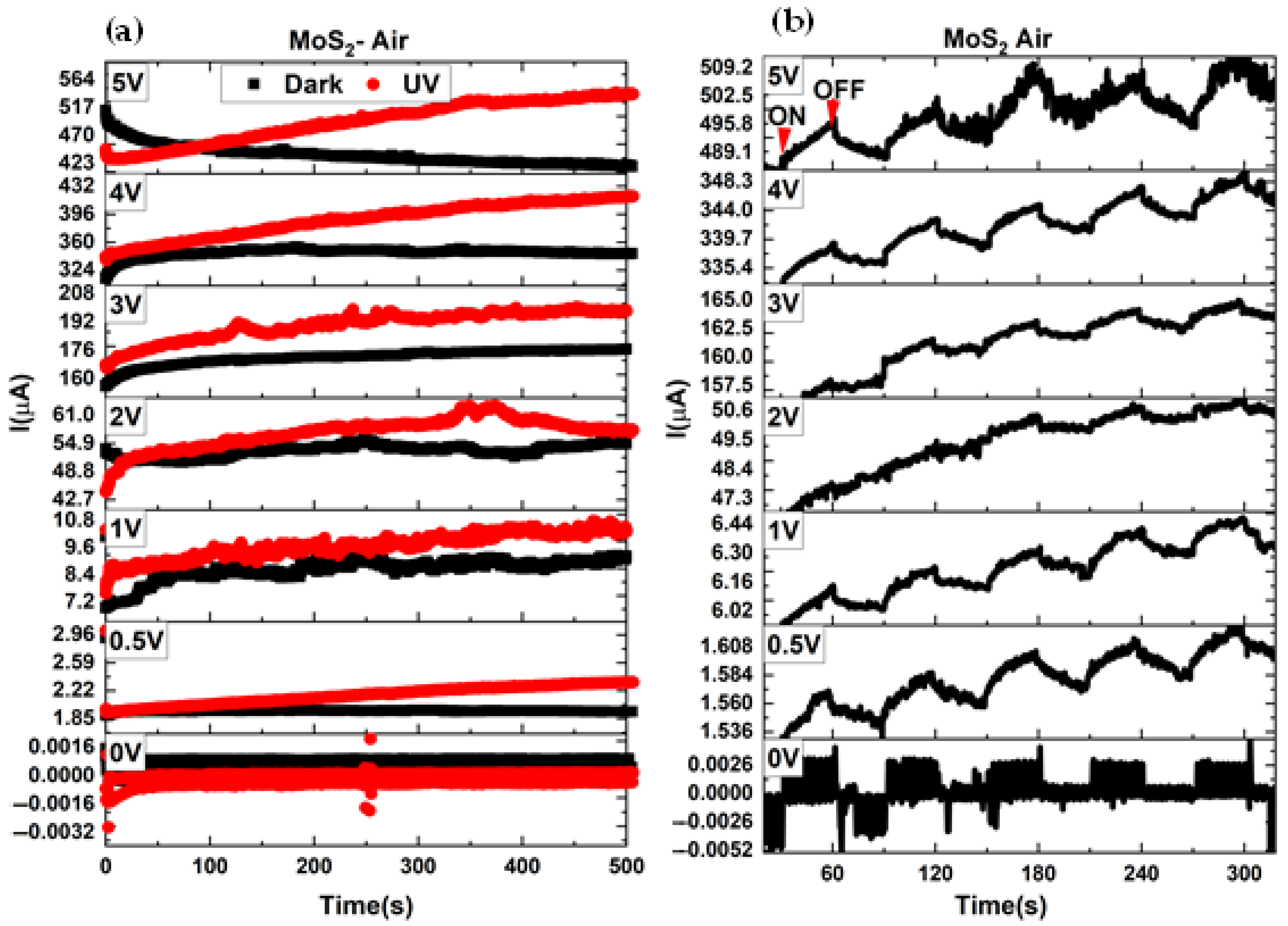
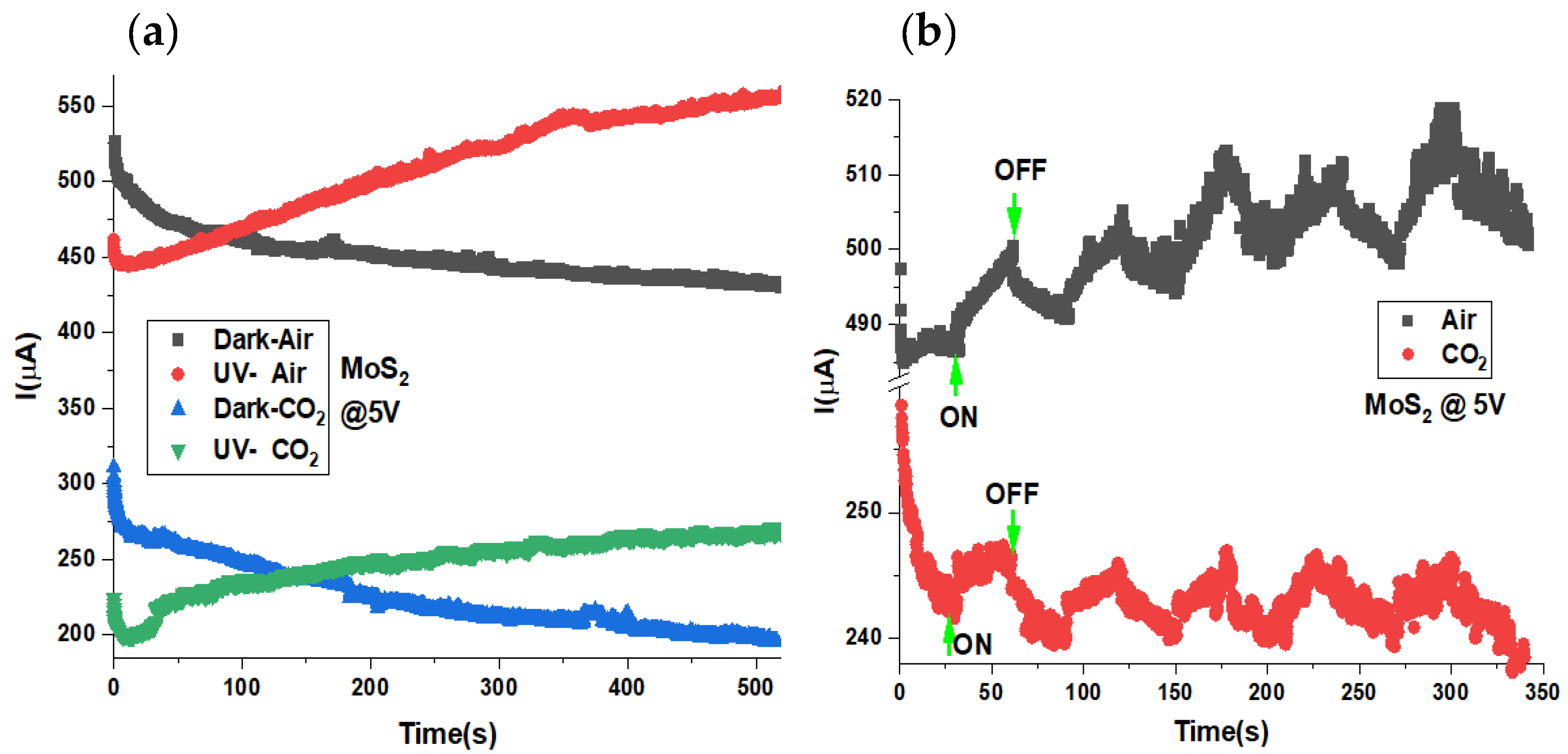
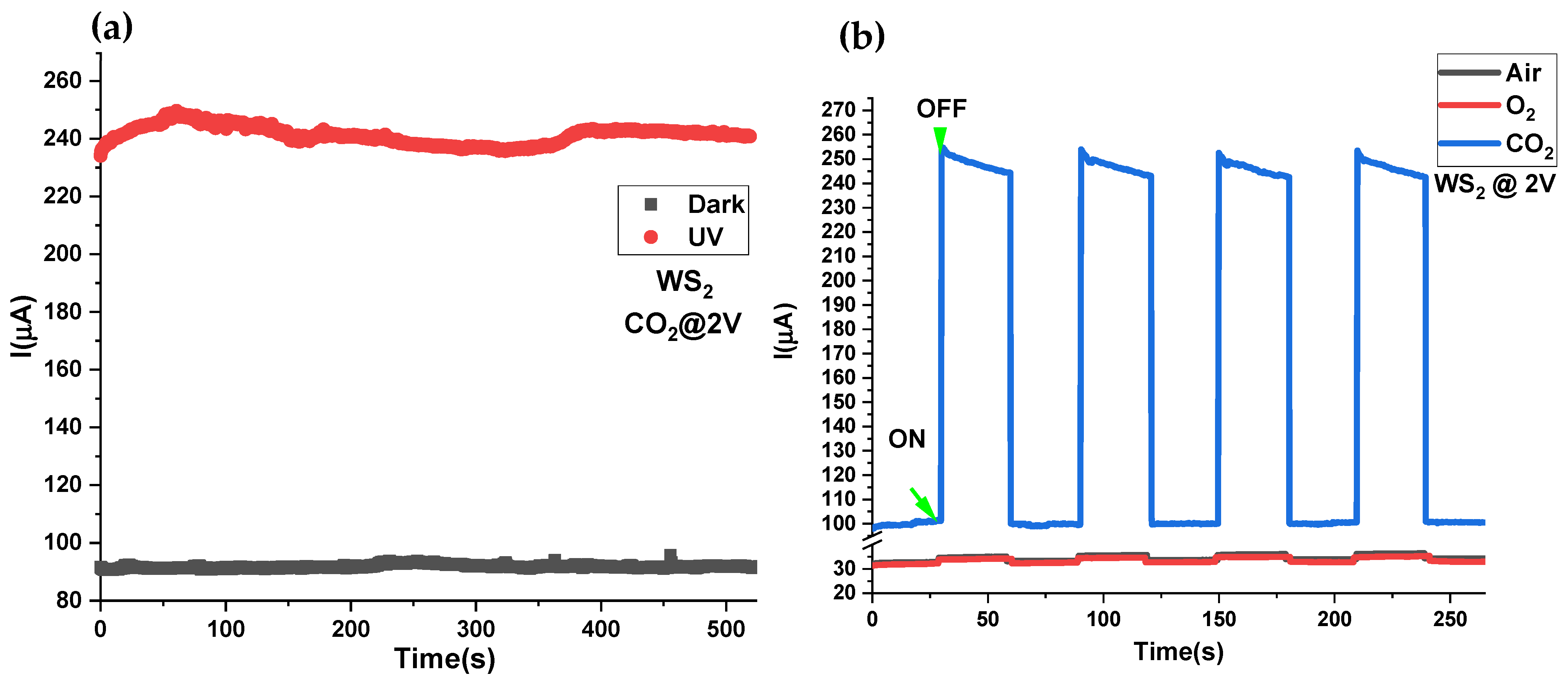
3.6. Transient Response

The MoS2 and WS2 thin-film response and recovery time under UV illumination of 365 nm are c depicted in Figure 14. The MoS2 and WS2 on–off behavior gives us a sense of the rise and fall with time under dark and illumination conditions. The response/rise time was calculated when the source of light opened, and when the light was turned off, the recovery/decay time was measured. The MoS2 thin film has a longer recovery time and faster response time in an air environment, as in Figure 14a. However, under CO2 stimuli, a longer response/recovery time is noted. The longer response time may refer to the CO2 gas adsorption on MoS2, which is faster than the desorption kinetics. The observed response/recovery time of MoS2 is in seconds, which limits the application of the MoS2 photodetector. However, for the WS2 thin film, a faster response is observed, as in Figure 14b. Generally, the WS2 thin film introduced a shorter response time than the recovery time. In addition, shorter response and recovery times are observed for the CO2 case compared with air and O2 stimuli. The CO2 adsorption/desorption kinetics on WS2 are faster than in the air and O2 gas cases. The adsorption energy and diffusion coefficient of O2 were the lowest [63].

3.7. Photocurrent Gain (Pg), Photoresponsivity ( R λ ), External Quantum Efficiency (EQE) and Detectivity ( D * )

Some other parameters may contribute to the general performance of the photodetector sensor, such as photocurrent gain (Pg), photoresponsivity ( R λ ), external quantum efficiency (EQE), and detectivity ( D * ). I ph = I Light I Dark gives the induced photocurrent I ph , where I ph increases as the applied voltage and light power increase [64]. Here, the light intensity is maintained at a consistent level and excitation wavelength of 365 nm. Photocurrent gain (Pg), responsivity ( R λ ), and external quantum efficiency can be calculated as reported before [23,24,65,66]. The detectable signal is another significant figure of merit for a photodetector referred by the specific detectivity [67]. The parameters of I ph , Pg, R λ , EQE, and D * for MoS2 and WS2 thin films are reported in Table 3. It seems that the general performance of MoS2 is weaker than WS2 thin film. The I ph of MoS2 is decreased by introducing CO2 as explained in Figure 8. Consequently, all the other parameters will get affected in a similar way. The EQE of MoS2 thin film under air is higher than that in CO2.
The photocurrent and photocurrent gain of MoS2 and WS2 under air and CO2 are represented in Figure 15. For WS2 film, a clear enhancement in both photocurrent and photocurrent gain is observed under CO2 stimuli. In the case of WS2 thin film, we introduced a p-type semiconductor with a large carrier concentration value of 5,500,000,000,000 cm−2; consequently, a high photocurrent is observed in the air. We observed a large enhancement in the EQE in the air of 2,200,000 compared with CO2 of 162,000,000, due to the fact that CO2 is an oxidizing agent interacting with p-type semiconductor materials, which can improve the electron concentrations and increase the conductivity of the film, as in Figure 15b [68]. Under O2 stimuli, we observed a lower responsivity of 0.915 µA/mW. On the other hand, for the MoS2 thin film, we have an n-type semiconductor that is interacting with oxidizing CO2 gas, which will increase the film resistance and consequently decrease the photocurrent, as in Figure 15a.

4. Conclusions

A 2D transition metal dichalcogenide heterojunctions of MoS2 and WS2 on silicon substrates for optoelectronic applications have been introduced. Using commercial chemical and physical vapor deposition techniques, we combined them for large-scale photodetector applications and beyond. For the first time, we exposed CO2 and O2 gases through a designed chamber to test their effects on the UV photodetector applications. The semiconducting behavior of MoS2 and WS2 thin films are n- and p-type with sheet carrier concentrations of 3,500,000,000,000 and 5,500,000,000,000 cm−2. The WS2 thin film showed higher carrier mobility of 2980 cm2/V compared to 946 cm2/V of MoS2 film. WS2 showed a fast response under UV illumination than MoS2 under air, CO2, and O2 environments. The calculated detectivity of WS2 showed higher values compared to the air and O2 adsorbed gases. We also observed that the EQE of WS2 under CO2 is 162,000,000 compared with 6,740,000 for the case of MoS2 thin film. Our findings provide high motivation for using MoS2 and WS2 thin films for space and industrial applications filled with environmental gases.zzzz

Author Contributions

Conceptualization, M.A.B. and S.E.Z.; methodology, M.A.B. and S.E.Z.; validation, M.A.B., S.E.Z., Y.R.E., M.Y., N.A., M.T., G.F.A. and M.S.; formal analysis, M.A.B., S.E.Z., Y.R.E., M.S. and M.Y.; investigation, M.A.B., S.E.Z., M.Y., M.T., N.A., M.S. and Y.R.E.; resources, M.A.B., Ş.A., S.E.Z., M.Y., Y.R.E., N.A., G.F.A. and M.S.; data curation, M.A.B., Ş.A., S.E.Z., N.A. and M.S.; writing—original draft preparation, M.A.B., S.E.Z. and M.Y.; writing—review and editing, M.A.B., S.E.Z., Y.R.E., M.Y., M.T., N.A., G.F.A. and M.S.; visualization, M.A.B., Ş.A., N.A., G.F.A. and M.S.; supervision, M.A.B., Y.R.E. and M.Y.; project administration, M.A.B., Ş.A., N.A. and M.S.; funding acquisition, M.A.B., N.A. and M.S. All authors have read and agreed to the published version of the manuscript.

Funding

Princess Nourah bint Abdulrahman University Researchers Supporting Project (PNURSP2022R291), Princess Nourah bint Abdulrahman University, Riyadh, Saudi Arabia.

Data Availability Statement

Not applicable.

Acknowledgments

The authors express their gratitude to Princess Nourah bint Abdulrahman University Researchers Supporting Project (PNURSP2022R291), Princess Nourah bint Abdulrahman University, Riyadh, Saudi Arabia. The first and the second authors would like to thank the Abdus Salam International Centre for Theoretical Physics (ICTP) Trieste TS, Italy for the building discussions, support, and tremendous multidisciplinary talks and events.

Conflicts of Interest

The authors declare no conflict of interest.

References

  1. Gonzaalez-Cuevas, J.A.; Refaat, T.F.; Abedin, M.N.; Elsayed-Ali, H.E. Modeling of the Temperature-Dependent Spectral Response of In_{1−x}Ga_{x}Sb Infrared Photodetectors. Opt. Eng. 2006, 45, 44001. [Google Scholar]
  2. Basyooni, M.A.; Shaban, M.; El Sayed, A.M. Enhanced Gas Sensing Properties of Spin-coated Na-doped ZnO Nanostructured Films. Sci. Rep. 2017, 7, 41716. [Google Scholar] [CrossRef] [PubMed] [Green Version]
  3. Zaki, S.E.; Basyooni, M.A. Ultra-sensitive gas sensor based fano resonance modes in periodic and fibonacci quasi-periodic Pt/PtS2 structures. Sci. Rep. 2022, 12, 9759. [Google Scholar] [CrossRef] [PubMed]
  4. Zaki, S.E.; Basyooni, M.A.; Shaban, M.; Rabia, M.; Eker, Y.R.; Attia, G.F.; Yilmaz, M.; Ahmed, A.M. Role of oxygen vacancies in vanadium oxide and oxygen functional groups in graphene oxide for room temperature CO2 gas sensors. Sens. Actuators A Phys. 2019, 294, 17–24. [Google Scholar] [CrossRef]
  5. Owen, T. The Composition and Early History of the Atmosphere of Mars; Mars Publication: Hong Kong, China, 2018; pp. 818–834. [Google Scholar]
  6. Elías, A.L.; Perea-López, N.; Castro-Beltrán, A.; Berkdemir, A.; Lv, R.; Feng, S.; Long, A.D.; Hayashi, T.; Kim, Y.A.; Endo, M.; et al. Controlled synthesis and transfer of large-area WS2 sheets: From single layer to few layers. ACS Nano 2013, 7, 5235–5242. [Google Scholar] [CrossRef]
  7. Huo, N.; Yang, S.; Wei, Z.; Li, S.S.; Xia, J.B.; Li, J. Photoresponsive and Gas Sensing Field-Effect Transistors based on Multilayer WS2 Nanoflakes. Sci. Rep. 2014, 4, 5209. [Google Scholar] [CrossRef] [PubMed] [Green Version]
  8. Georgiou, T.; Jalil, R.; Belle, B.D.; Britnell, L.; Gorbachev, R.V.; Morozov, S.V.; Kim, Y.J.; Gholinia, A.; Haigh, S.J.; Makarovsky, O.; et al. Vertical field-effect transistor based on graphene-WS2 heterostructures for flexible and transparent electronics. Nat. Nanotechnol. 2013, 8, 100–103. [Google Scholar] [CrossRef]
  9. Bernardi, M.; Palummo, M.; Grossman, J.C. Extraordinary sunlight absorption and one nanometer thick photovoltaics using two-dimensional monolayer materials. Nano Lett. 2013, 13, 3664–3670. [Google Scholar] [CrossRef]
  10. Park, J.; Kim, M.S.; Cha, E.; Kim, J.; Choi, W. Synthesis of uniform single layer WS2 for tunable photoluminescence. Sci. Rep. 2017, 7, 16121. [Google Scholar] [CrossRef] [Green Version]
  11. Das, U.; Bhattacharjee, S.; Mahato, B.; Prajapat, M.; Sarkar, P.; Roy, A. Uniform, large-scale growth of WS2 nanodomains via CVD technique for stable non-volatile RRAM application. Mater. Sci. Semicond. Process. 2020, 107, 104837. [Google Scholar] [CrossRef]
  12. Lin, Y.; Adilbekova, B.; Firdaus, Y.; Yengel, E.; Faber, H.; Sajjad, M.; Zheng, X.; Yarali, E.; Seitkhan, A.; Bakr, O.M.; et al. 17% Efficient Organic Solar Cells Based on Liquid Exfoliated WS2 as a Replacement for PEDOT:PSS. Adv. Mater. 2019, 31, 1902965. [Google Scholar] [CrossRef]
  13. Sharma, D.; Motayed, A.; Shah, P.B.; Amani, M.; Georgieva, M.; Glen Birdwell, A.; Dubey, M.; Li, Q.; Davydov, A. V Transfer characteristics and low-frequency noise in single- and multi-layer MoS2 field-effect transistors. Appl. Phys. Lett. 2015, 107, 162102. [Google Scholar] [CrossRef]
  14. Nicolosi, V.; Chhowalla, M.; Kanatzidis, M.G.; Strano, M.S.; Coleman, J.N. Liquid exfoliation of layered materials. Science 2013, 340, 1226419. [Google Scholar] [CrossRef] [Green Version]
  15. Coleman, J.N. ChemInform Abstract: Two-Dimensional Nanosheets Produced by Liquid Exfoliation of Layered Materials. ChemInform 2011, 42, 568–571. [Google Scholar] [CrossRef]
  16. Yu, X.; Prévot, M.S.; Sivula, K. Multiflake thin film electronic devices of solution processed 2D MoS2 enabled by sonopolymer assisted exfoliation and surface modification. Chem. Mater. 2014, 26, 5892–5899. [Google Scholar] [CrossRef]
  17. Paton, K.R.; Varrla, E.; Backes, C.; Smith, R.J.; Khan, U.; O’Neill, A.; Boland, C.; Lotya, M.; Istrate, O.M.; King, P.; et al. Scalable production of large quantities of defect-free few-layer graphene by shear exfoliation in liquids. Nat. Mater. 2014, 13, 624–630. [Google Scholar] [CrossRef]
  18. Varrla, E.; Backes, C.; Paton, K.R.; Harvey, A.; Gholamvand, Z.; McCauley, J.; Coleman, J.N. Large-scale production of size-controlled MoS2 nanosheets by shear exfoliation. Chem. Mater. 2015, 27, 1129–1139. [Google Scholar] [CrossRef]
  19. Knirsch, K.C.; Berner, N.C.; Nerl, H.C.; Cucinotta, C.S.; Gholamvand, Z.; McEvoy, N.; Wang, Z.; Abramovic, I.; Vecera, P.; Halik, M.; et al. Basal-Plane Functionalization of Chemically Exfoliated Molybdenum Disulfide by Diazonium Salts. ACS Nano 2015, 9, 6018–6030. [Google Scholar] [CrossRef] [PubMed]
  20. Eda, G.; Yamaguchi, H.; Voiry, D.; Fujita, T.; Chen, M.; Chhowalla, M. Photoluminescence from chemically exfoliated MoS2. Nano Lett. 2011, 11, 5111–5116. [Google Scholar] [CrossRef] [PubMed]
  21. Yang, X.Y. Photoenergy and Thin Film Materials; John Wiley & Sons: Hoboken, NJ, USA, 2019. [Google Scholar]
  22. Giannazzo, F.; Lara Avila, S.; Eriksson, J.; Sonde, S. Integration of 2D Materials for Electronics Applications. Crystals 2019, 7, 162. [Google Scholar]
  23. Ali, M.; Mohamed, B. VO2 Ince Film Içeren Iki Boyutlu Ve Çok Katmanli Yapilardaki Arayüzey Gerilmelerinin Termokromik Ve Fotodetektör Performanslara Etkisi. Ph.D. Thesis, Necmettin Erbakan University, Konya, Turkey, 2020. [Google Scholar]
  24. Basyooni, M.A.; Zaki, S.E.; Shaban, M.; Eker, Y.R.; Yilmaz, M. Efficient MoWO3/VO2/MoS2/Si UV Schottky photodetectors; MoS2 optimization and monoclinic VO2 surface modifications. Sci. Rep. 2020, 10, 15926. [Google Scholar] [CrossRef] [PubMed]
  25. Yu, J.; Li, J.; Zhang, W.; Chang, H. Synthesis of high quality two-dimensional materials via chemical vapor deposition. Chem. Sci. 2015, 6, 6705–6716. [Google Scholar] [CrossRef] [PubMed]
  26. Cai, Z.; Liu, B.; Zou, X.; Cheng, H.M. Chemical Vapor Deposition Growth and Applications of Two-Dimensional Materials and Their Heterostructures. Chem. Rev. 2018, 118, 6091–6133. [Google Scholar] [CrossRef] [PubMed]
  27. Wang, H.; Yu, L.; Lee, Y.H.; Fang, W.; Hsu, A.; Herring, P.; Chin, M.; Dubey, M.; Li, L.J.; Kong, J.; et al. Large-scale 2D electronics based on single-layer MoS2 grown by chemical vapor deposition. In Proceedings of the Technical Digest—International Electron Devices Meeting, IEDM, San Francisco, CA, USA, 10–13 December 2012. [Google Scholar]
  28. Browning, R.; Padigi, P.; Solanki, R.; Tweet, D.J.; Schuele, P.; Evans, D. Atomic layer deposition of MoS2 thin films. Mater. Res. Express 2015, 2, 025006. [Google Scholar] [CrossRef]
  29. Loh, T.A.J.; Chua, D.H.C. Growth mechanism of pulsed laser fabricated few-layer MoS2 on metal substrates. ACS Appl. Mater. Interfaces 2014, 6, 15966–15971. [Google Scholar] [CrossRef] [PubMed]
  30. Serrao, C.R.; Diamond, A.M.; Hsu, S.L.; You, L.; Gadgil, S.; Clarkson, J.; Carraro, C.; Maboudian, R.; Hu, C.; Salahuddin, S. Highly crystalline MoS2 thin films grown by pulsed laser deposition. Appl. Phys. Lett. 2015, 106, 052101. [Google Scholar] [CrossRef]
  31. Basyooni, M.A.; Al-Dossari, M.; Zaki, S.E.; Eker, Y.R.; Yilmaz, M.; Shaban, M. Tuning the Metal–Insulator Transition Properties of VO2 Thin Films with the Synergetic Combination of Oxygen Vacancies, Strain Engineering, and Tungsten Doping. Nanomaterials 2022, 12, 1470. [Google Scholar] [CrossRef] [PubMed]
  32. Ma, X.; Shi, M. Thermal evaporation deposition of few-layer MoS2 films. Nano-Micro Lett. 2013, 5, 135–139. [Google Scholar] [CrossRef]
  33. Wu, S.; Huang, C.; Aivazian, G.; Ross, J.S.; Cobden, D.H.; Xu, X. Vapor-solid growth of high optical quality MoS2 monolayers with near-unity valley polarization. ACS Nano 2013, 7, 2768–2772. [Google Scholar] [CrossRef] [PubMed] [Green Version]
  34. Pacley, S.; Hu, J.; Jespersen, M.; Hilton, A.; Waite, A.; Brausch, J.; Beck-Millerton, E.; Voevodin, A.A. Impact of reduced graphene oxide on MoS2 grown by sulfurization of sputtered MoO3 and Mo precursor films. J. Vac. Sci. Technol. A Vac. Surf. Film. 2016, 34, 041505. [Google Scholar] [CrossRef]
  35. Hussain, S.; Shehzad, M.A.; Vikraman, D.; Khan, M.F.; Singh, J.; Choi, D.C.; Seo, Y.; Eom, J.; Lee, W.G.; Jung, J. Synthesis and characterization of large-area and continuous MoS2 atomic layers by RF magnetron sputtering. Nanoscale 2016, 8, 4340–4347. [Google Scholar] [CrossRef] [PubMed]
  36. Matsuura, K.; Ohashi, T.; Muneta, I.; Ishihara, S.; Kakushima, K.; Tsutsui, K.; Ogura, A.; Wakabayashi, H. Low-Carrier-Density Sputtered MoS2 Film by Vapor-Phase Sulfurization. J. Electron. Mater. 2018, 47, 3497–3501. [Google Scholar] [CrossRef]
  37. Furchi, M.M.; Polyushkin, D.K.; Pospischil, A.; Mueller, T. Mechanisms of photoconductivity in atomically thin MoS2. Nano Lett. 2014, 14, 6165–6170. [Google Scholar] [CrossRef] [PubMed] [Green Version]
  38. Han, P.; Adler, E.R.; Liu, Y.; St Marie, L.; El Fatimy, A.; Melis, S.; van Keuren, E.; Barbara, P. Ambient effects on photogating in MoS2 photodetectors. Nanotechnology 2019, 30, 284004. [Google Scholar] [CrossRef] [Green Version]
  39. Pospischil, A.; Mueller, T. Optoelectronic devices based on atomically thin transition metal dichalcogenides. Appl. Sci. 2016, 6, 78. [Google Scholar] [CrossRef] [Green Version]
  40. Klement, P.; Steinke, C.; Chatterjee, S.; Wehling, T.O.; Eickhoff, M. Effects of the Fermi level energy on the adsorption of O2 to monolayer MoS2. 2D Mater. 2018, 5, 045025. [Google Scholar] [CrossRef]
  41. Kumar, R.; Zheng, W.; Liu, X.; Zhang, J.; Kumar, M. MoS2-Based Nanomaterials for Room-Temperature Gas Sensors. Adv. Mater. Technol. 2020, 5, 1901062. [Google Scholar] [CrossRef]
  42. Khan, M.A.; Kumawat, K.L.; Nanda, K.K.; Krupanidhi, S.B. Reduced graphene oxide-based broad band photodetector and temperature sensor: Effect of gas adsorption on optoelectrical properties. J. Nanoparticle Res. 2018, 20, 293. [Google Scholar] [CrossRef] [Green Version]
  43. Yan, H.J.; Xu, B.; Shi, S.Q.; Ouyang, C.Y. First-principles study of the oxygen adsorption and dissociation on graphene and nitrogen doped graphene for Li-air batteries. J. Appl. Phys. 2012, 112, 112602. [Google Scholar] [CrossRef]
  44. Guo, R.; Han, D.; Chen, W.; Dai, L.; Ji, K.; Xiong, Q.; Li, S.; Reb, L.K.; Scheel, M.A.; Pratap, S.; et al. Degradation mechanisms of perovskite solar cells under vacuum and one atmosphere of nitrogen. Nat. Energy 2021, 6, 977–986. [Google Scholar] [CrossRef]
  45. Karataş, A.; Yılmaz, M. Molybdenum disulfide thin films fabrication from multi-phase molybdenum oxide using magnetron sputtering and CVD systems together. Superlattices Microstruct. 2020, 143, 106555. [Google Scholar] [CrossRef]
  46. Basyooni, M.A.; Eker, Y.R.; Yilmaz, M. Van-der Waals 2-Dimensional Nanostructured Molybdenum and Tungsten Disulfide-Si Heterostructure Photodetector under Different Environment Stimuli for High Yield Optoelectronics. Mühendislik Bilimleri 2020, 2. [Google Scholar]
  47. Shanmugam, M.; Durcan, C.A.; Yu, B. Layered semiconductor molybdenum disulfide nanomembrane based Schottky-barrier solar cells. Nanoscale 2012, 4, 7399–7405. [Google Scholar] [CrossRef] [PubMed]
  48. Basyooni, M.A.; Zaki, S.E.; Tihtih, M.; Eker, Y.R.; Ateş, Ş. Photonic bandgap engineering in (VO2)n/(WSe2)nphotonic superlattice for versatile near- and mid-infrared phase transition applications. J. Phys. Condens. Matter 2022, 34, 325901. [Google Scholar] [CrossRef] [PubMed]
  49. Splendiani, A.; Sun, L.; Zhang, Y.; Li, T.; Kim, J.; Chim, C.Y.; Galli, G.; Wang, F. Emerging photoluminescence in monolayer MoS2. Nano Lett. 2010, 10, 1271–1275. [Google Scholar] [CrossRef] [PubMed]
  50. Zhu, Z.Y.; Cheng, Y.C.; Schwingenschlögl, U. Giant spin-orbit-induced spin splitting in two-dimensional transition-metal dichalcogenide semiconductors. Phys. Rev. B Condens. Matter Mater. Phys. 2011, 84, 153402. [Google Scholar] [CrossRef] [Green Version]
  51. Zhao, W.; Ghorannevis, Z.; Chu, L.; Toh, M.; Kloc, C.; Tan, P.H.; Eda, G. Evolution of electronic structure in atomically thin sheets of ws2 and wse2. ACS Nano 2013, 7, 791–797. [Google Scholar] [CrossRef] [Green Version]
  52. Yuan, L.; Huang, L. Exciton dynamics and annihilation in WS2 2D semiconductors. Nanoscale 2015, 7, 7402–7408. [Google Scholar] [CrossRef]
  53. Hwang, J.D.; Chang, W.T.; Chen, Y.H.; Kung, C.Y.; Hu, C.H.; Chen, P.S. Suppressing the dark current of metal-semiconductor-metal SiGe/Si heterojunction photodetector by using asymmetric structure. Thin Solid Films 2007, 515, 3837–3839. [Google Scholar] [CrossRef]
  54. Liu, D.; Wang, Q.; Shen, W.; Wang, D. Self-cleaning antireflective coating with a hierarchical texture for light trapping in micromorph solar cells. J. Mater. Chem. C 2017, 5, 103–109. [Google Scholar] [CrossRef]
  55. Chang, K.; Chen, W.; Ma, L.; Li, H.; Li, H.; Huang, F.; Xu, Z.; Zhang, Q.; Lee, J.Y. Graphene-like MoS2/amorphous carbon composites with high capacity and excellent stability as anode materials for lithium ion batteries. J. Mater. Chem. 2011, 21, 6251–6257. [Google Scholar] [CrossRef]
  56. He, H.Y. Assembly of 1T-WSe2: Sn nanosheets/graphene by a modified hydrothermal process for water splitting. J. Sol-Gel Sci. Technol. 2020, 93, 554–562. [Google Scholar] [CrossRef]
  57. Xiong, M.; Qian, J.; Yang, K.; Chen, Z.; Mei, T.; Wang, J.; Li, J.; Yu, L.; Wang, X. Efficient polysulfide anchor: Brain coral-like WS2 nanosheets. J. Mater. Sci. 2020, 55, 12031–12040. [Google Scholar] [CrossRef]
  58. Ko, T.S.; Huang, C.C.; Lin, D.Y. Optical and transport properties of Ni-MoS2. Appl. Sci. 2016, 6, 227. [Google Scholar] [CrossRef] [Green Version]
  59. Method of Making an Integrated Photodetector in Which a Silicon Nitride Layer Forms an Anti-Reflective Film and Part of Multi-Layer Insulator within Transistor Structures. U.S. Patents US6803249B2, 12 October 2014. Available online: https://patents.google.com/patent/US6803249B2/en (accessed on 2 July 2020).
  60. Oliva, N.; Casu, E.A.; Yan, C.; Krammer, A.; Rosca, T.; Magrez, A.; Stolichnov, I.; Schueler, A.; Martin, O.J.F.; Ionescu, A.M. van der Waals MoS2/VO2 heterostructure junction with tunable rectifier behavior and efficient photoresponse. Sci. Rep. 2017, 7, 14250. [Google Scholar] [CrossRef] [PubMed] [Green Version]
  61. Basyooni, M.A.; Zaki, S.E.; Ertugrul, S.; Yilmaz, M.; Eker, Y.R. Fast response of CO2 room temperature gas sensor based on Mixed-Valence Phases in Molybdenum and Tungsten Oxide nanostructured thin films. Ceram. Int. 2020, 46, 9839–9853. [Google Scholar] [CrossRef]
  62. Tongay, S.; Zhou, J.; Ataca, C.; Liu, J.; Kang, J.S.; Matthews, T.S.; You, L.; Li, J.; Grossman, J.C.; Wu, J. Broad-range modulation of light emission in two-dimensional semiconductors by molecular physisorption gating. Nano Lett. 2013, 13, 2831–2836. [Google Scholar] [CrossRef] [PubMed]
  63. Wang, Y.; Hu, X.; Guo, T.; Tian, W.; Hao, J.; Guo, Q. The competitive adsorption mechanism of CO2, H2O and O2 on a solid amine adsorbent. Chem. Eng. J. 2021, 416, 129007. [Google Scholar] [CrossRef]
  64. Ko, P.J.; Abderrahmane, A.; Kim, N.H.; Sandhu, A. High-performance near-infrared photodetector based on nano-layered MoSe2. Semicond. Sci. Technol. 2017, 32, 065015. [Google Scholar] [CrossRef]
  65. Wu, J.M.; Chang, W.E. Ultrahigh responsivity and external quantum efficiency of an ultraviolet-light photodetector based on a single VO2 microwire. ACS Appl. Mater. Interfaces 2014, 6, 14286–14292. [Google Scholar] [CrossRef] [PubMed]
  66. Chao, C.-H.; Weng, W.-J.; Wei, D.-H. Enhanced UV photodetector response and recovery times using a nonpolar ZnO sensing layer. J. Vac. Sci. Technol. A Vac. Surf. Films 2016, 34, 02D106. [Google Scholar] [CrossRef]
  67. Liu, X.; Gu, L.; Zhang, Q.; Wu, J.; Long, Y.; Fan, Z. All-printable band-edge modulated ZnO nanowire photodetectors with ultra-high detectivity. Nat. Commun. 2014, 5, 4007. [Google Scholar] [CrossRef] [PubMed] [Green Version]
  68. Bachmeier, A.; Hall, S.; Ragsdale, S.W.; Armstrong, F.A. Selective visible-light-driven CO2 reduction on a p-type dye-sensitized nio photocathode. J. Am. Chem. Soc. 2014, 136, 13518–13521. [Google Scholar] [CrossRef] [PubMed]
Scheme 1. Electrical and optoelectrical systems under different gas environments and different temperature conditions.
Nanomaterials 12 03585 sch001
Figure 1. (a,b) Raman spectra of MoS2 and WS2 on Si substrates, respectively.
Nanomaterials 12 03585 g001
Figure 2. (a,b) PL spectra of MoS2 and WS2 on Si substrates, respectively.
Nanomaterials 12 03585 g002
Figure 3. (a) MoS2 and (b) WS2 thin-film optical microscopy images.
Nanomaterials 12 03585 g003
Figure 4. (a,b) FE-SEM morphology of MoS2 and WS2 thin films.
Nanomaterials 12 03585 g004
Figure 5. AFM topography and the horizontal line profile: (a,b) 3D topography images and corresponding line profile of MoS2 and WS2 samples, respectively.
Nanomaterials 12 03585 g005
Figure 6. (a,b) General XPS survey spectrum distributions of both MoS2 and WS2 thin films.
Nanomaterials 12 03585 g006
Figure 7. The MoS2 and WS2 photodetector under the illumination of UV light and the device’s actual image as seen through the probe station. The measurements were carried out in the air, O2, and CO2 environments.
Nanomaterials 12 03585 g007
Figure 8. I-V characteristic of MoS2 in the absence of light and UV illumination conditions under air and CO2.
Nanomaterials 12 03585 g008
Figure 9. (a) Photocurrent behavior with time of MoS2 under dark and UV illumination conditions in air, and (b) the on–off time-resolved photoresponse of MoS2 thin film under bias voltages of 0–5 V.
Nanomaterials 12 03585 g009
Figure 10. (a,b) Photocurrent behavior with time and on–off time-resolved photoresponse of MoS2 thin film under dark and UV illumination conditions in both air and 50 sccm CO2 environments at a bias voltage of 5 V.
Nanomaterials 12 03585 g010
Figure 11. Characteristic I-V curve of WS2 under dark and UV illumination conditions under (a) air environment, (b) O2 environment and (c) CO2 environment.
Nanomaterials 12 03585 g011aNanomaterials 12 03585 g011b
Figure 12. (a) Photocurrent behavior with the time of WS2 thin film under a dark condition in the air at a different bias voltage of 0, 0.5, 1, and 2 V. (b) The on–off dynamics of the current with a time of WS2 thin film in air and 50 sccm O2 environments under a different bias voltage of 0–2 V.
Nanomaterials 12 03585 g012
Figure 13. (a) Photocurrent behavior with time of WS2 thin film under dark and UV conditions in CO2 at a bias voltage of 2 V. (b) The on–off dynamics of the photoresponse with a time of WS2 thin film in air, 50 sccm O2, and 50 sccm CO2 environments under a bias voltage of 2 V.
Nanomaterials 12 03585 g013
Figure 14. Shows the response and therecovery times for (a) MoS2 and (b) WS2 thin films under gas stimuli.
Nanomaterials 12 03585 g014
Figure 15. (a,b) Photocurrent and photocurrent gain of MoS2 and WS2 thin film under gas stimuli.
Nanomaterials 12 03585 g015
Table 1. AFM roughness parameters of MoS2 and WS2 samples.
SampleRegionMin (nm)Max (nm)Mid (nm)Rq (nm)Ra (nm)Rz (nm)RskRku
MoS2Line−24.58422.080−1.25246.66410.6899.20045.3290.439
WS2Line−4.9646.6820.85911.6462.7612.09911.374−0.645
Table 2. Room-temperature surface resistance and Hall-effect measurements for MoS2 and WS2 on a silicon substrate.
SampleRs
(Ω/sq)
Rho
(/Ω-cm)
VH
(V)
RH
(m3/C)
TypeNs/Ps
(/cm2)
N/P
(/cm3)
Mobility
(cm2/V)
MoS218900.00284−0.0129−0.00000268N−3,500,000,000,000−2,330,000,000,000,000,000946
WS238,2000.05730.008190.00000171P5,500,000,000,0003,670,000,000,000,000,0002980
Table 3. The photocurrent ( I ph ), photocurrent gain (Pg), photoresponsivity ( R λ ), external quantum efficiency (EQE), and detectivity ( D * ) of MoS2 and WS2 samples.
SampleGasPhotocurrent
(A)
Photocurrent Gain (a.u.)Responsivity
(µA/mW)
EQE D *
MoS2Air0.00001310.02706.574513,900,000372.05
CO20.000006350.02653.17656,740,000256.34
WS2Air0.000002070.06311.0352,200,000225.76
CO20.0001531.5176.50162,000,0009509.10
O20.000001830.05680.9151,940,000201.34
Publisher’s Note: MDPI stays neutral with regard to jurisdictional claims in published maps and institutional affiliations.

