

Indirect Band Gap in Scrolled MoS2 Monolayers

 , , , , , and
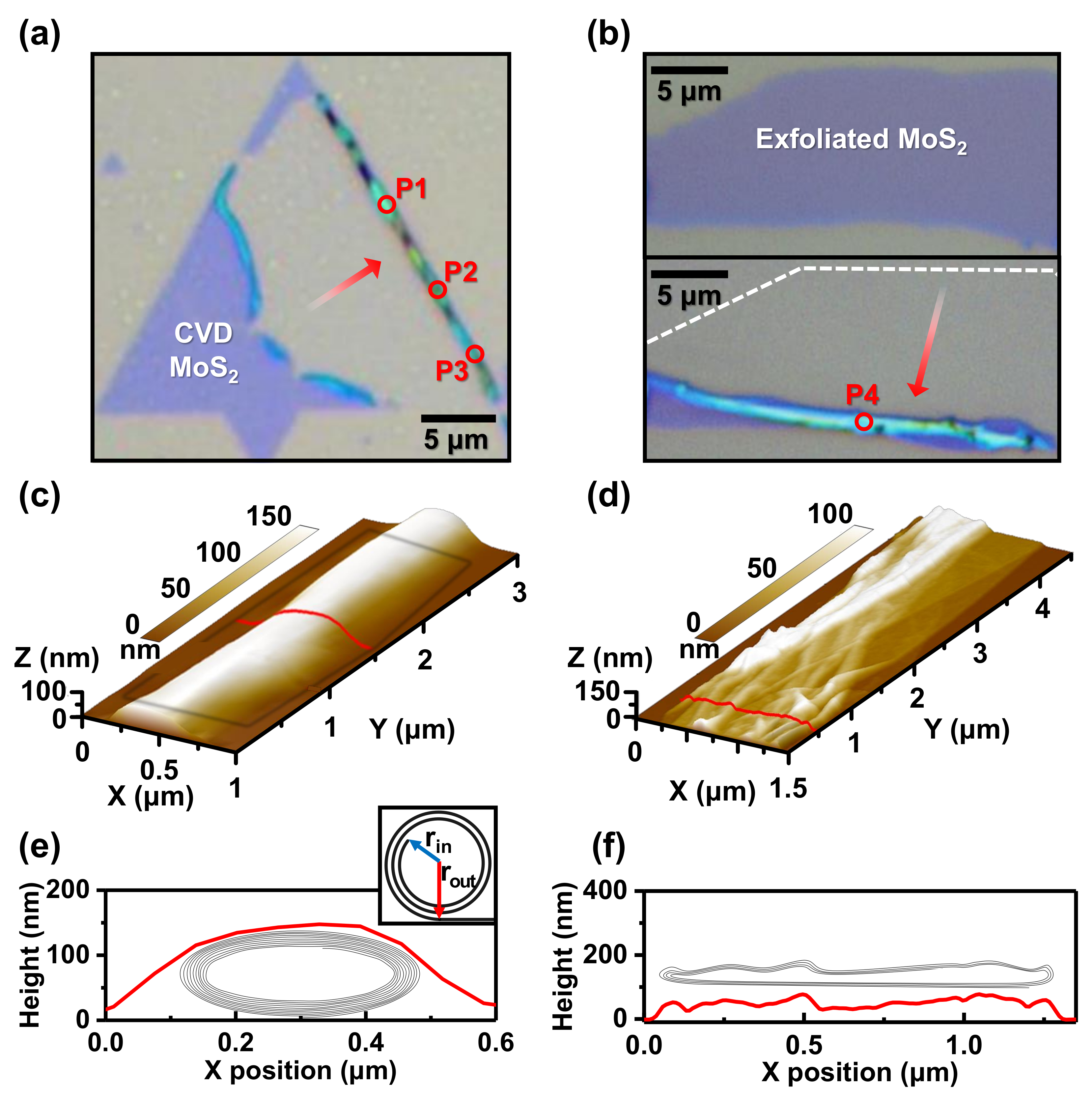
Abstract
1. Introduction
2. Materials and Methods
3. Results and Discussion
3.1. Structure of Scrolled MoS2
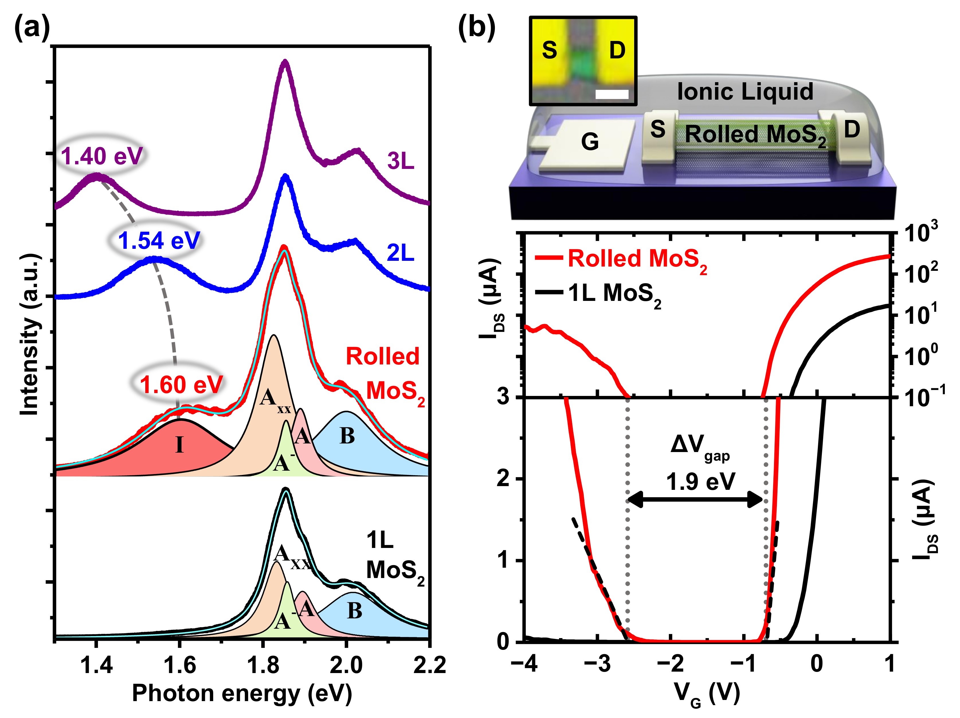
3.2. Band Gap of Scrolled MoS
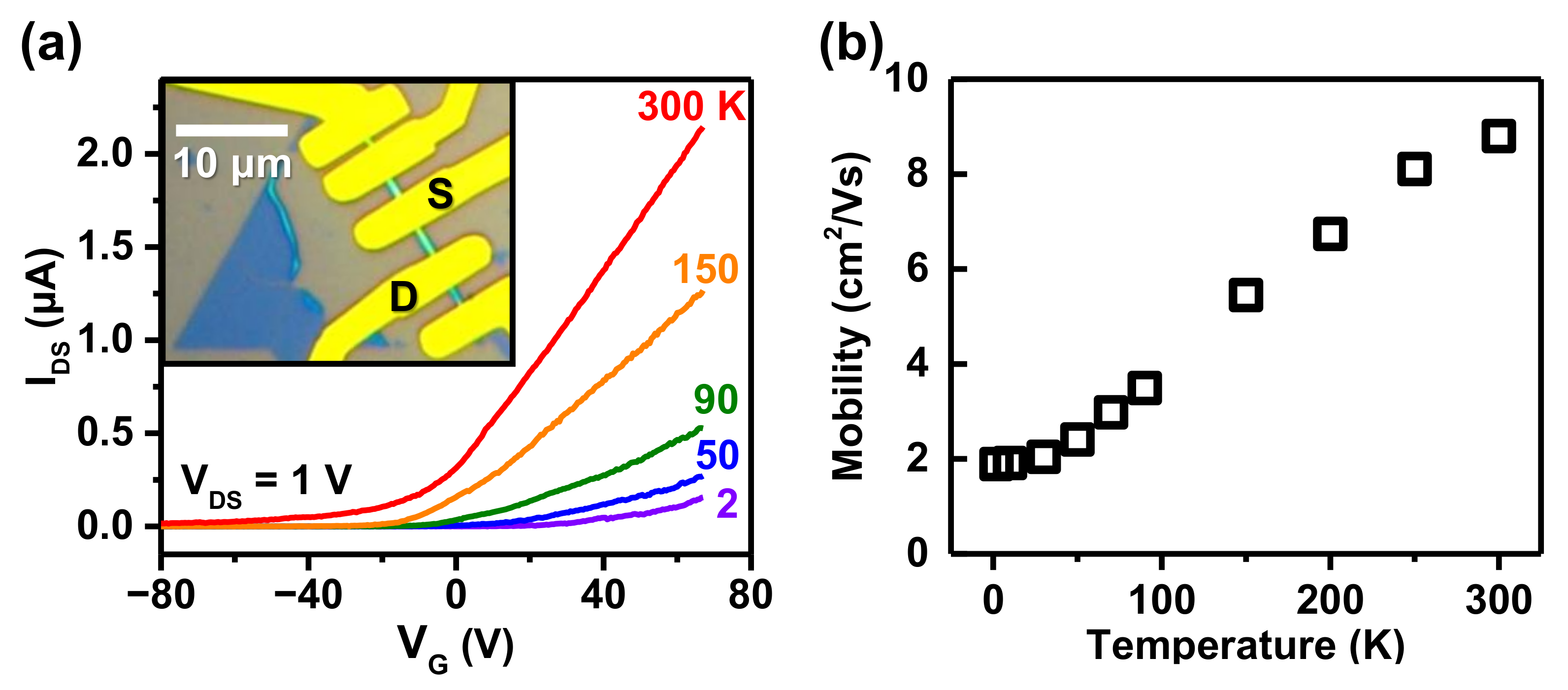
3.3. Back-Gated Field Effect Transistor Based on Scrolled MoS
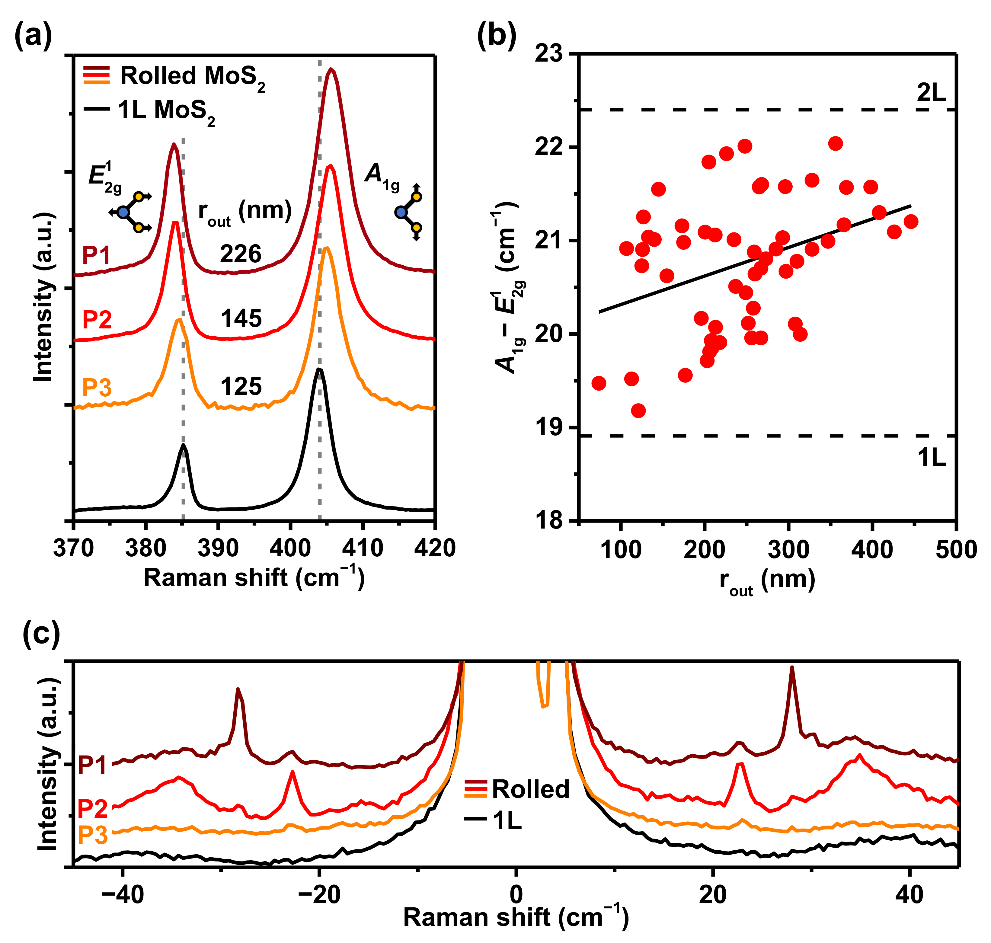
3.4. Raman Spectra of Scrolled MoS
4. Conclusions
Author Contributions
Funding
Data Availability Statement
Conflicts of Interest
References
- Manzeli, S.; Ovchinnikov, D.; Pasquier, D.; Yazyev, O.V.; Kis, A. 2D transition metal dichalcogenides. Nat. Rev. Mater. 2017, 2, 17033. [Google Scholar] [CrossRef]
- Deng, S.; Gao, E.; Xu, Z.; Berry, V. Adhesion energy of MoS2 thin films on silicon-based substrates determined via the attributes of a single MoS2 wrinkle. ACS Appl. Mater. Interfaces 2017, 9, 7812–7818. [Google Scholar] [CrossRef] [PubMed]
- Castellanos-Gomez, A.; van der Zant, H.S.; Steele, G.A. Folded MoS2 layers with reduced interlayer coupling. Nano Res. 2014, 7, 572–578. [Google Scholar] [CrossRef]
- Xie, X.; Ju, L.; Feng, X.; Sun, Y.; Zhou, R.; Liu, K.; Fan, S.; Li, Q.; Jiang, K. Controlled fabrication of high-quality carbon nanoscrolls from monolayer graphene. Nano Lett. 2009, 9, 2565–2570. [Google Scholar] [CrossRef]
- Xu, B.; Lin, X.; Mei, Y. Versatile rolling origami to fabricate functional and smart materials. Cell Rep. Phys. Sci. 2020, 1, 100244. [Google Scholar] [CrossRef]
- Uhm, T.; Na, J.; Lee, J.U.; Cheong, H.; Lee, S.W.; Campbell, E.E.; Jhang, S.H. Structural configurations and Raman spectra of carbon nanoscrolls. Nanotechnology 2020, 31, 315707. [Google Scholar] [CrossRef]
- Baptista-Pires, L.; Orozco, J.; Guardia, P.; Merkoçi, A. Architecting graphene oxide rolled-up micromotors: A simple paper-based manufacturing technology. Small 2018, 14, 1702746. [Google Scholar] [CrossRef]
- Liu, Y.; Wang, L.; Zhang, H.; Ran, F.; Yang, P.; Li, H. Graphene oxide scroll meshes encapsulated Ag nanoparticles for humidity sensing. RSC Adv. 2017, 7, 40119–40123. [Google Scholar] [CrossRef]
- Suh, D.H.; Hwang, D.Y. Formation of hexagonal boron nitride nanoscrolls induced by inclusion and exclusion of self-assembling molecules in solution process. Nanoscale 2014, 6, 5686–5690. [Google Scholar]
- Cui, X.; Kong, Z.; Gao, E.; Huang, D.; Hao, Y.; Shen, H.; Di, C.a.; Xu, Z.; Zheng, J.; Zhu, D. Rolling up transition metal dichalcogenide nanoscrolls via one drop of ethanol. Nat. Commun. 2018, 9, 1301. [Google Scholar] [CrossRef]
- Hao, S.; Yang, B.; Gao, Y. Fracture-induced nanoscrolls from CVD-grown monolayer molybdenum disulfide. Phys. Status Solidi (RRL) Rapid Res. Lett. 2016, 10, 549–553. [Google Scholar] [CrossRef]
- Meng, J.; Wang, G.; Li, X.; Lu, X.; Zhang, J.; Yu, H.; Chen, W.; Du, L.; Liao, M.; Zhao, J.; et al. Rolling up a monolayer MoS2 sheet. Small 2016, 12, 3770–3774. [Google Scholar] [CrossRef] [PubMed]
- Wang, Z.; Wu, H.H.; Li, Q.; Besenbacher, F.; Zeng, X.C.; Dong, M. Self-scrolling MoS2 metallic wires. Nanoscale 2018, 10, 18178–18185. [Google Scholar] [CrossRef]
- Deng, W.; Chen, X.; Li, Y.; You, C.; Chu, F.; Li, S.; An, B.; Ma, Y.; Liao, L.; Zhang, Y. Strain Effect Enhanced Ultrasensitive MoS2 Nanoscroll Avalanche Photodetector. J. Phys. Chem. Lett. 2020, 11, 4490–4497. [Google Scholar] [CrossRef] [PubMed]
- Qian, Q.; Zu, R.; Ji, Q.; Jung, G.S.; Zhang, K.; Zhang, Y.; Buehler, M.J.; Kong, J.; Gopalan, V.; Huang, S. Chirality-Dependent Second Harmonic Generation of MoS2 Nanoscroll with Enhanced Efficiency. ACS Nano 2020, 14, 13333–13342. [Google Scholar] [CrossRef] [PubMed]
- Fang, X.; Wei, P.; Wang, L.; Wang, X.; Chen, B.; He, Q.; Yue, Q.; Zhang, J.; Zhao, W.; Wang, J.; et al. Transforming monolayer transition-metal dichalcogenide nanosheets into one-dimensional nanoscrolls with high photosensitivity. ACS Appl. Mater. Interfaces 2018, 10, 13011–13018. [Google Scholar] [CrossRef] [PubMed]
- Zhao, B.; Wan, Z.; Liu, Y.; Xu, J.; Yang, X.; Shen, D.; Zhang, Z.; Guo, C.; Qian, Q.; Li, J.; et al. High-order superlattices by rolling up van der Waals heterostructures. Nature 2021, 591, 385–390. [Google Scholar] [CrossRef] [PubMed]
- Zhang, S.; Gao, F.; Feng, W.; Yang, H.; Hu, Y.; Zhang, J.; Xiao, H.; Li, Z.; Hu, P. High-responsivity photodetector based on scrolling monolayer MoS2 hybridized with carbon quantum dots. Nanotechnology 2021, 33, 105301. [Google Scholar] [CrossRef]
- Yue, Q.; Wang, L.; Fan, H.; Zhao, Y.; Wei, C.; Pei, C.; Song, Q.; Huang, X.; Li, H. Wrapping plasmonic silver nanoparticles inside one-dimensional nanoscrolls of transition-metal dichalcogenides for enhanced photoresponse. Inorg. Chem. 2020, 60, 4226–4235. [Google Scholar] [CrossRef]
- Wang, L.; Yue, Q.; Pei, C.; Fan, H.; Dai, J.; Huang, X.; Li, H.; Huang, W. Scrolling bilayer WS2/MoS2 heterostructures for high-performance photo-detection. Nano Res. 2020, 13, 959–966. [Google Scholar] [CrossRef]
- Jiang, Z.; Zhou, W.; Hong, A.; Guo, M.; Luo, X.; Yuan, C. MoS2 Moiré superlattice for hydrogen evolution reaction. ACS Energy Lett. 2019, 4, 2830–2835. [Google Scholar] [CrossRef]
- Khaledian, M.; Ismail, R.; Akbari, E. Band structures of graphene nanoscrolls and their dispersion relation near the Fermi point. RSC Adv. 2016, 6, 38753–38760. [Google Scholar] [CrossRef]
- Wang, Y.; Jiang, C.; Chen, Q.; Zhou, Q.; Wang, H.; Wan, J.; Ma, L.; Wang, J. Highly promoted carrier mobility and intrinsic stability by rolling up monolayer black phosphorus into nanoscrolls. J. Phys. Chem. Lett. 2018, 9, 6847–6852. [Google Scholar] [CrossRef]
- Xiao, J.; Long, M.; Li, X.; Xu, H.; Huang, H.; Gao, Y. Theoretical prediction of electronic structure and carrier mobility in single-walled MoS2 nanotubes. Sci. Rep. 2014, 4, 4327. [Google Scholar] [CrossRef]
- Desai, S.B.; Madhvapathy, S.R.; Amani, M.; Kiriya, D.; Hettick, M.; Tosun, M.; Zhou, Y.; Dubey, M.; Ager III, J.W.; Chrzan, D.; et al. Gold-mediated exfoliation of ultralarge optoelectronically-perfect monolayers. Adv. Mater. 2016, 28, 4053–4058. [Google Scholar] [CrossRef] [PubMed]
- Pandey, J.; Soni, A. Unraveling biexciton and excitonic excited states from defect bound states in monolayer MoS2. Appl. Surf. Sci. 2019, 463, 52–57. [Google Scholar] [CrossRef]
- Pugno, N.M. The design of self-collapsed super-strong nanotube bundles. J. Mech. Phys. Solids 2010, 58, 1397–1410. [Google Scholar] [CrossRef]
- Shi, X.; Pugno, N.M.; Gao, H. Tunable core size of carbon nanoscrolls. J. Comput. Theor. Nanosci. 2010, 7, 517–521. [Google Scholar] [CrossRef]
- Liu, Z.; Gao, J.; Zhang, G.; Cheng, Y.; Zhang, Y.W. From two-dimensional nano-sheets to roll-up structures: Expanding the family of nanoscroll. Nanotechnology 2017, 28, 385704. [Google Scholar] [CrossRef]
- Blees, M.K.; Barnard, A.W.; Rose, P.A.; Roberts, S.P.; McGill, K.L.; Huang, P.Y.; Ruyack, A.R.; Kevek, J.W.; Kobrin, B.; Muller, D.A.; et al. Graphene kirigami. Nature 2015, 524, 204–207. [Google Scholar] [CrossRef]
- Reynolds, M.F.; McGill, K.L.; Wang, M.A.; Gao, H.; Mujid, F.; Kang, K.; Park, J.; Miskin, M.Z.; Cohen, I.; McEuen, P.L. Capillary origami with atomically thin membranes. Nano Lett. 2019, 19, 6221–6226. [Google Scholar] [CrossRef] [PubMed]
- Splendiani, A.; Sun, L.; Zhang, Y.; Li, T.; Kim, J.; Chim, C.Y.; Galli, G.; Wang, F. Emerging photoluminescence in monolayer MoS2. Nano Lett. 2010, 10, 1271–1275. [Google Scholar] [CrossRef] [PubMed]
- Liu, K.; Zhang, L.; Cao, T.; Jin, C.; Qiu, D.; Zhou, Q.; Zettl, A.; Yang, P.; Louie, S.G.; Wang, F. Evolution of interlayer coupling in twisted molybdenum disulfide bilayers. Nat. Commun. 2014, 5, 4966. [Google Scholar] [CrossRef] [PubMed]
- Li, Y.; Qi, Z.; Liu, M.; Wang, Y.; Cheng, X.; Zhang, G.; Sheng, L. Photoluminescence of monolayer MoS2 on LaAlO3 and SrTiO3 substrates. Nanoscale 2014, 6, 15248–15254. [Google Scholar] [CrossRef]
- Shi, W.; Ye, J.; Zhang, Y.; Suzuki, R.; Yoshida, M.; Miyazaki, J.; Inoue, N.; Saito, Y.; Iwasa, Y. Superconductivity series in transition metal dichalcogenides by ionic gating. Sci. Rep. 2015, 5, 12534. [Google Scholar] [CrossRef] [PubMed]
- Braga, D.; Gutieérrez Lezama, I.; Berger, H.; Morpurgo, A.F. Quantitative determination of the band gap of WS2 with ambipolar ionic liquid-gated transistors. Nano Lett. 2012, 12, 5218–5223. [Google Scholar] [CrossRef] [PubMed]
- Berghäuser, G.; Malic, E. Analytical approach to excitonic properties of MoS2. Phys. Rev. B 2014, 89, 125309. [Google Scholar] [CrossRef]
- Ponomarev, E.; Pásztor, Á.; Waelchli, A.; Scarfato, A.; Ubrig, N.; Renner, C.; Morpurgo, A.F. Hole transport in exfoliated monolayer MoS2. ACS Nano 2018, 12, 2669–2676. [Google Scholar] [CrossRef]
- Ponomarev, E.; Gutiérrez-Lezama, I.; Ubrig, N.; Morpurgo, A.F. Ambipolar light-emitting transistors on chemical vapor deposited monolayer MoS2. Nano Lett. 2015, 15, 8289–8294. [Google Scholar] [CrossRef]
- Chu, L.; Schmidt, H.; Pu, J.; Wang, S.; Özyilmaz, B.; Takenobu, T.; Eda, G. Charge transport in ion-gated mono-, bi-and trilayer MoS2 field effect transistors. Sci. Rep. 2014, 4, 7293. [Google Scholar] [CrossRef]
- Zhang, C.; Gong, C.; Nie, Y.; Min, K.A.; Liang, C.; Oh, Y.J.; Zhang, H.; Wang, W.; Hong, S.; Colombo, L.; et al. Systematic study of electronic structure and band alignment of monolayer transition metal dichalcogenides in Van der Waals heterostructures. 2D Mater. 2016, 4, 015026. [Google Scholar] [CrossRef]
- Huang, Y.L.; Chen, Y.; Zhang, W.; Quek, S.Y.; Chen, C.H.; Li, L.J.; Hsu, W.T.; Chang, W.H.; Zheng, Y.J.; Chen, W.; et al. Bandgap tunability at single-layer molybdenum disulphide grain boundaries. Nat. Commun. 2015, 6, 6298. [Google Scholar] [CrossRef] [PubMed]
- Schmidt, H.; Wang, S.; Chu, L.; Toh, M.; Kumar, R.; Zhao, W.; Castro Neto, A.; Martin, J.; Adam, S.; Özyilmaz, B.; et al. Transport properties of monolayer MoS2 grown by chemical vapor deposition. Nano Lett. 2014, 14, 1909–1913. [Google Scholar] [CrossRef]
- Li, H.; Zhang, Q.; Yap, C.C.R.; Tay, B.K.; Edwin, T.H.T.; Olivier, A.; Baillargeat, D. From bulk to monolayer MoS2: Evolution of Raman scattering. Adv. Funct. Mater. 2012, 22, 1385–1390. [Google Scholar] [CrossRef]
- Huang, S.; Liang, L.; Ling, X.; Puretzky, A.A.; Geohegan, D.B.; Sumpter, B.G.; Kong, J.; Meunier, V.; Dresselhaus, M.S. Low-frequency interlayer Raman modes to probe interface of twisted bilayer MoS2. Nano Lett. 2016, 16, 1435–1444. [Google Scholar] [CrossRef] [PubMed]
- Lloyd, D.; Liu, X.; Christopher, J.W.; Cantley, L.; Wadehra, A.; Kim, B.L.; Goldberg, B.B.; Swan, A.K.; Bunch, J.S. Band gap engineering with ultralarge biaxial strains in suspended monolayer MoS2. Nano Lett. 2016, 16, 5836–5841. [Google Scholar] [CrossRef]
- Zhang, X.; Han, W.; Wu, J.; Milana, S.; Lu, Y.; Li, Q.; Ferrari, A.; Tan, P. Raman spectroscopy of shear and layer breathing modes in multilayer MoS2. Phys. Rev. B 2013, 87, 115413. [Google Scholar] [CrossRef]


Publisher’s Note: MDPI stays neutral with regard to jurisdictional claims in published maps and institutional affiliations. |
© 2022 by the authors. Licensee MDPI, Basel, Switzerland. This article is an open access article distributed under the terms and conditions of the Creative Commons Attribution (CC BY) license (https://creativecommons.org/licenses/by/4.0/).
Share and Cite
Na, J.; Park, C.; Lee, C.H.; Choi, W.R.; Choi, S.; Lee, J.-U.; Yang, W.; Cheong, H.; Campbell, E.E.B.; Jhang, S.H. Indirect Band Gap in Scrolled MoS2 Monolayers. Nanomaterials 2022, 12, 3353. https://doi.org/10.3390/nano12193353
Na J, Park C, Lee CH, Choi WR, Choi S, Lee J-U, Yang W, Cheong H, Campbell EEB, Jhang SH. Indirect Band Gap in Scrolled MoS2 Monolayers. Nanomaterials. 2022; 12(19):3353. https://doi.org/10.3390/nano12193353
Chicago/Turabian StyleNa, Jeonghyeon, Changyeon Park, Chang Hoi Lee, Won Ryeol Choi, Sooho Choi, Jae-Ung Lee, Woochul Yang, Hyeonsik Cheong, Eleanor E. B. Campbell, and Sung Ho Jhang. 2022. "Indirect Band Gap in Scrolled MoS2 Monolayers" Nanomaterials 12, no. 19: 3353. https://doi.org/10.3390/nano12193353
APA StyleNa, J., Park, C., Lee, C. H., Choi, W. R., Choi, S., Lee, J.-U., Yang, W., Cheong, H., Campbell, E. E. B., & Jhang, S. H. (2022). Indirect Band Gap in Scrolled MoS2 Monolayers. Nanomaterials, 12(19), 3353. https://doi.org/10.3390/nano12193353