Abstract
Silver nanowires (AgNWs) are used as transparent electrodes (TE) in many devices. However, the contact mode between the nanowires is the biggest reason why the sheet resistance of silver nanowires is limited. Here, simple and effective ultraviolet (UV) irradiation welding is chosen to solve this problem. The influence of the power density of the UV irradiation on welding of the silver nanowires is studied and the fixed irradiation time is chosen as one minute. The range of the UV (380 nm) irradiation power is chosen from 30 mW/cm2 to 150 mW/cm2. First of all, the transmittance of the silver nanowire film is not found to be affected by the UV welding (400–11,000 nm). The sheet resistance of the silver nanowires decreases to 73.9% at 60 mW/cm2 and increases to 127.6% at 120 mW/cm2. The investigations on the UV irradiation time reveal that the sheet resistance of the AgNWs decreases continuously when the UV irradiation time is varied from 0 to 3 min, and drops to 57.3% of the initial value at 3 min. From 3–6 min of the continuous irradiation time, the change of the sheet resistance is not obvious, which reflects the self-limiting and self-termination of AgNWs welding. By changing the wavelength of the UV irradiation from 350–400 nm, it is found that the welding effect is best when the UV wavelength is 380 nm. The average transmittance, square resistance, and the figure of merit of the welded AgNWs at 400–780 nm are 95.98%, 56.5 Ω/sq, and 117.42 × 10⁻⁴ Ω−1, respectively. The UV-welded AgNWs are also used in silicon-based photodetectors, and the quantum efficiency of the device is improved obviously.
1. Introduction
The rapid development in flexible transparent electrodes (TE) has opened up possibilities for using them in a wide range of applications, such as optoelectronic devices. At present, many devices still use indium tin oxide (ITO) as a transparent electrode. This is because ITO has excellent conductivity (10–20 Ω/sq) and high transparency (transmittance of 90%) [1]. However, ITO is brittle, and its constituent raw materials are scarce. These factors prevent ITO from being widely used in future flexible optoelectronic devices [2,3,4,5]. Overall, this impacts the development of flexible electronic devices.
In order to overcome these limitations, a number of alternative transparent electrode materials have been suggested for replacing ITO, including carbon nanotubes (CNTs) [6], graphene [7], metal grids [8], copper and silver metal nanowires [9,10], and electrospun metal nanofibers. Among the transparent conductive films (TCFs), metal nanowires, especially AgNWs, exhibit superior performance, including low sheet resistance (10–20 Ω/sq), and high transparency (80–90%) [11,12,13]. Moreover, it can also be applied to flexible devices, which widens its application range greatly. However, AgNW-based TCFs exhibit some drawbacks including high surface roughness, high resistance between the AgNW junctions, and weak adhesion to various substrates. Furthermore, AgNW-based TCFs are easily oxidized when they are exposed to water or air, which results in a sharp increase in the sheet resistance [14,15].
In recent years, the optimization of AgNWs has been widely studied. The sheet resistance of AgNWs depends on the close connection at the junction [16], and the contact resistance at the junction strongly affects the total sheet resistance of AgNWs electrodes. Through welding, the sheet resistance and the roughness of the film can be reduced without reducing the transmittance of the AgNWs. Many welding methods have been proposed, such as thermal welding [17], plasmonic welding [18,19], chemical welding [20,21,22], and UV irradiation welding [23]. Among these, the UV irradiation welding does not cause other effects on the film compared to the other welding methods. It also does not produce a large amount of heat to damage the substrate. The UV irradiation welding, therefore, has a better potential of improving the properties of AgNWs films. Liang et al. studied the efficient welding of AgNWs by using ultraviolet A (UVA) nano-photothermal process with A wavelength range of ~320 to ~400 nm [23]. They obtained AgNWs with a low sheet resistance of 25 Ω/sq, a high transmittance of 90%, and exhibiting excellent flexibility. KOU et al. found that the AgNWs network still achieved sheet resistance of less than 20 Ω/sq, transmittance of ~87% at 550 nm wavelength, and good mechanical flexibility after 1 h or more of sunlight exposure [24]. During the UV welding, the light-induced welding was a self-limiting process due to the gradually weakened plasmonic effect during the formation of nanowire joints. However, the current experimental light sources mostly have a fixed optical power and a broad spectral range. Therefore, there is a lack of systematic research on the optical power density and irradiation wavelength of UV irradiation.
In this work, the light power irradiated on the film was changed with a fixed irradiation time of 1 min. It was found that when the UV power irradiated on the AgNWs was too high, the resulting sheet resistance was also high. At the same time, the silver nanowires were irradiated by the UV light at 60 mW/cm2 for 0–6 min. After the irradiation for 1 min, the initial welding of the AgNWs occurred, and the wire-to-wire contact changed significantly as compared to that before the welding. After 3 min of the irradiation, the welding was basically over, and the sheet resistance did not change significantly. Under the condition of changing the wavelength of the UV light, the most suitable UV wavelength was determined by comparing the change of sheet resistance. Finally, the soldered AgNWs were applied to silicon-based photodetectors.
2. Materials and Methods
2.1. Preparation of the AgNWs
AgNWs with diameters of 30 nm were purchased from KECHUANG. In this experiment, 2.0 mg/mL AgNWs were selected. In order to avoid an uneven dispersion of the AgNWs, the reagent had to be placed on the vortex mixer and was made to vibrate for 1 min before the spin coating. The AgNWs were then spread all over the BaF2 substrate with a pipette. In order to evenly distribute the solution on the substrate, the homogenizer should be started after the solution on the substrate is stationary for 10 s. The speed of the homogenizer is 1500 r/min, and the time is 1 min.
2.2. UV Irradiation Welding of AgNWs
The UV irradiation process is shown in Figure 1. The AgNWs film coated on BaF2 substrate was irradiated by a Microenerg 500 W UV light source. The distance between the sample and the UV light source was adjusted by a lifting platform to control the light power density of the UV lamp. As can be seen in Figure 1, the overlapping regions of the silver nanowires will become more tightly connected when exposed to UV radiation. The wavelength of the UV lamp was controlled by the filter installed in the light outlet.
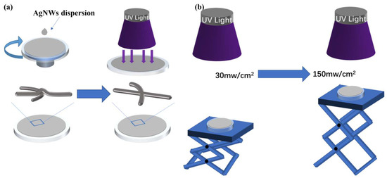
Figure 1.
Schematic diagram of the UV irradiation of AgNWs. (a) Schematic diagram of welding principle. (b) Schematic diagram of optical power regulation principle.
2.3. Characterization
The optical transmittance spectra were obtained by using a spectrophotometer (Lambda 950, Perkin Elmer, MA, USA) and Fourier infrared spectrometer (VERTEX 70V, BRUKER, Saarbrücken, Germany). The sheet resistance and the electrical properties of the films were measured by a four-probe square resistance tester (ST2558B-F01, SUZHOU JINGGE, Suzhou, China). Field emission scanning electron microscopy (SEM, Zeiss, Sigma300, Oberkochen, Germany) was also used to investigate the microstructure of thin films. The optical power shining on the sample was measured by an optical power meter (Thorlabs, PM160, Newton, MA, USA).
3. Results and Discussion
3.1. Optical Properties
It is well known that the two absorption peaks of AgNWs in the UV-visible range generally appear at about 350 and 380 nm, which is derived from the plasmon resonance of AgNWs, similar to bulk silver film and the transverse plasmon mode of AgNWs, respectively [25,26]. Optical properties are one of the most important properties of transparent conductive films. Figure 2 shows the transmittance curve of AgNWs on the BaF2 substrate after 0–6 min of the UV irradiation.
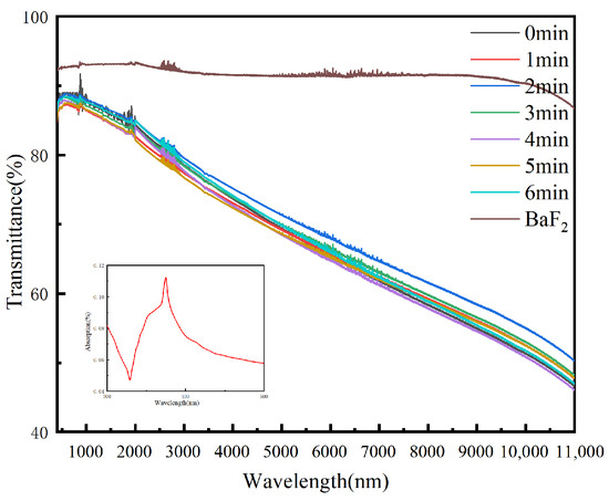
Figure 2.
Transmittance of AgNWs with different UV irradiation times (400–11,000 nm). Insert of the figure shows the absorption of AgNWs at 300–500 nm.
As can be seen from the figure, the transmittance of AgNW film has not been affected significantly after the UV irradiation (380 nm, 60 mW/cm2) at different irradiation times. It also does not exhibit any appreciable change compared to that before the irradiation. When AgNWs network is irradiated by the UV light, surface plasmon resonance is generated, which is a photothermal effect on AgNWs network. This increases the local temperature of AgNWs network and forms a so-called “hot spot” [27]. Therefore, the way the UV light is irradiated on the sample does not affect the transmittance of AgNWs. The results presented in Figure 2 also prove this phenomenon. With the change of irradiation time, the transmittance fluctuates only slightly irregularly, which may be caused by the subtle differences between the samples coated with spins and the substrate preparation process. At the same time, when the influence of other factors of the UV welding on the transmittance of AgNWs are investigated, the same conclusions are drawn.
3.2. Electrical Properties
The most valuable benefit of the UV irradiation on AgNWs is to improve their electrical properties. The effects of the UV irradiation with different optical power densities on the properties of AgNWs are studied. The irradiation time is controlled at 1 min because the influence of the first minute of the irradiation on the AgNW film can be readily observed. The optical power density of the UV light varies from 30 to 150 mW/cm2. In order to avoid the error of sheet resistance affecting the experimental law, the relative sheet resistance value is adopted. It can be seen from Figure 3a (Rs/Rs0, Rs: real-time sheet resistance, Rs0: initial sheet resistance) that the Rs/Rs0 decreases to 0.70484 when the UV power density is 60 mW/cm2, and increases to 1.56775 when the UV power density is 150 mW/cm2. The increase in the sheet resistance can be attributed to the high power of the UV light accelerating the precipitation of degradation particles on the surface of the AgNWs. Accelerated oxidation and vulcanization by the UV light result in the presence of small nanoparticles and thus increase the sheet resistance [28]. When studying the effect of UV irradiation time on silver nanowire film, the UV power density is fixed as 60 mW/cm2. As can be seen from Figure 3b (380 nm, 60 mW/cm2), the change of the sheet resistance of the AgNWs is obvious in the first 3 min, and Rs/Rs0 reaches 0.56596 in the third minute. It can also be seen in Figure 3b that 3 min after the welding, the AgNW sheet resistance does not decrease further. This is due to the fact that the welding process of AgNWs has been concluded. This implies that the UV irradiation welding of AgNWs is a self-limiting process [14]. This characteristic, as compared to the heat-welding method [17] has an obvious advantage. It can be seen from Figure 3c that the fixed irradiation power is 60 mW/cm2 and the time is 3 min. When the UV wavelength is 380 nm, Rs/Rs0 is the lowest, which is the same as the UV absorption peak of AgNWs. This phenomenon also proves that the UV welding of the AgNWs depends on the absorption of the UV light. Table 1 shows the variation of square resistance of silver nanowires before and after welding under the influence of different factors.
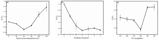
Figure 3.
Influence of different factors on the sheet resistance of the UV welded AgNWs. (a) Sheet resistance of AgNWs varies with the UV irradiation power. (b) Sheet resistance of AgNWs varies with the UV irradiation time. (c) Sheet resistance of AgNWs varies with the UV wavelength.

Table 1.
Variation of sheet resistance of AgNWs under ultraviolet irradiation under different influencing factors.
In Figure 3a, when the UV welding light power is too low, the influence on the film is relatively small, and the error bar is very small. However, with the gradual increase in the optical power, the welding effect and particle precipitation become more obvious, which also leads to the increase in the error bar. As shown in Figure 3b, with the extension of welding time, the error bar is large in the second minute because the welding is not completely completed, and the error bar is small when the welding is basically completed three minutes later. In Figure 3c, the error bar of the test results near the UV irradiation wavelength of 380 nm is small. This is caused by the strong absorption capacity of silver nanowires to 380 nm UV light, resulting in better welding results.
3.3. Figure of Merit
The transmittance and sheet resistance of transparent electrodes is of high importance for their application. The film transmittance and sheet resistance define the figure of merit of a transparent electrode. Haacke equation [29] is used for the calculation of the figure of merit, which is given as:
where Rsh is the average sheet resistance and T is the optical transmittance (here, transmittance has been averaged over the wavelength range of 400–11,000 nm). The ΦTC values of AgNWs films are shown in Figure 4 [30].
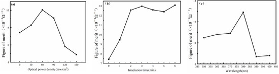
Figure 4.
Figure of merit diagram showing the influence of different factors on UV welding. (a) Optical power density (b) Irradiation time (c) Ultraviolet wavelength.
The results of the figure of merit calculation also confirm the previous conclusions. According to these results, it can be concluded that the best welding effect is obtained by selecting the optical power density of 60 mW/cm2, the irradiation time of 3 min, and the irradiation wavelength of 380 nm.
3.4. Microstructural Properties
SEM images give an insight into the welding process of AgNWs. Figure 5a–c show SEM images of the AgNWs welded for 0 min, 1 min, and 3 min, respectively. The areas highlighted by the black circles are where the silver nanowires are welded. Before the UV irradiation, the connection mode between the AgNWs is mostly lap connection, which is an important factor affecting its electrical properties. After 1 min of the UV irradiation, it can be seen that the AgNWs have changed from the lap to preliminary welding. At 3 min, the welding of the AgNWs is basically finished, and the welding degree is significantly higher than that observed for the irradiation time of 1 min. By comparing the effects of different UV irradiation times on the microstructure of AgNWs, it can be concluded that the UV irradiation plays a key role in the welding of the AgNWs.
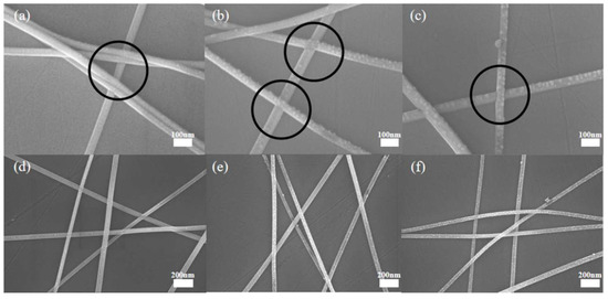
Figure 5.
SEM image of AgNWs: (a–c) are oblique (30°) SEM images to observe the overlapping of AgNWs, (d–f) are the inclined plane SEM images to observe the precipitation of AgNW small particles. (a,d) have UV irradiation for 0 min, (b,e) for 1 min, and (c,f) for 3 min.
Figure 5d–f are the inclined plane SEM images that were obtained for observing the precipitation of small particles of AgNWs. The surface of the AgNWs without the UV irradiation is smooth, and no small particles appear on the surface. When comparing the surface of AgNWs before and after the welding, it can be clearly seen that the precipitation of small nanoparticles on the surface increases significantly after the UV irradiation. This also indicates that the welding optimization and degradation effect of the UV irradiation on AgNWs occur simultaneously [28]. Figure 6 is a supplement to the previous microscopic morphological representation. Figure 6a mainly shows the welding effect of silver nanowires in many places, and Figure 6b mainly shows the phenomenon of particle precipitation after ultraviolet light irradiation.
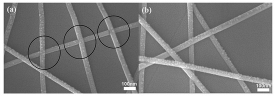
Figure 6.
SEM images of AgNWs irradiated by the UV light. (a) AgNW welding. (b) AgNWs precipitate small particles.
3.5. The Device Application
The AgNWs welding technology is applied to simple silicon devices [31]. The structure of the device is Ag/Si/AgNWs/Ag, in which the upper and lower silver are ring electrodes for eliciting test signals, the silver nanowire is coated on the upper surface of the whole silicon as a transparent electrode, and silicon is the active layer of the whole device. AgNW-contained solution is spin-coated on a Si substrate, which spontaneously forms a Schottky device. Compared with unwelded silver nanowires, due to the good transparency of the AgNWS conductive layer, more photons can be driven into the photoactive Si material, thus enhancing the light response. However, the contact between the welded silver nanowires and Si substrate is closer, and it provides more ways to transmit electrons. UV welding reduces the sheet resistance of the Ag nanowires. UV light is used to treat AgNWs coated on silicon, and a comparison of the device performance for two methods is made. It can be seen from Figure 7 that the quantum efficiency at 550 nm increases from 36.1% to 57.5% before and after the UV welding. The sheet resistance of the welded AgNWs decreases and more carriers are injected into the organic layer through the anode, thus improving the quantum efficiency of the device [32,33].
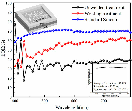
Figure 7.
Comparison of quantum efficiency of silicon devices before and after the UV welding. Insert of the figure shows the transmittance of AgNWs at 400–780 nm as well as the values of the average transmittance, the sheet resistance, the figure of merit after the irradiation, and the device structure diagram.
Since the transparent electrode of silver nanowire is generally located above the whole device, UV irradiation will affect the whole device. The effect is not too great when the photosensitive layer is more stable silicon, but should be discussed when UV sensitive materials act as photosensitive layers. For example, ZnO-based inverted quantum dot light-emitting diode (QLED) can improve the carrier injection of QLED after UV irradiation, which causes the device to exhibit high quantum efficiency [34]. However, some studies have shown that the perovskite materials in the perovskite base will decompose after UV irradiation, resulting in the reduction of the photostability of the device [35,36]. Therefore, before using UV irradiation welding, it is necessary to determine whether there is an effect on other layers of the device.
Based on the device performance comparison, it can be concluded that the UV welding can improve the performance of the device, which provides help for the fabrication of the device in the future. It should be noted here that the quantum efficiency value of the standard silicon is the standard value in this test system (the device structure and type of standard silicon are different from this device).
4. Conclusions
Influences of the UV irradiation power, time, and wavelength on the welding of AgNWs were studied. The welding of the AgNWs was realized based on the nanoscale photothermal process. Under the UVA irradiation, the sheet resistance of the AgNW films decreased rapidly within 3 min without affecting the optical transmittance. When the average transmittance of the AgNW films was 85.2% at 400–2000 nm and 76.6% at 2000–10,000 nm, the sheet resistance of the AgNW films decreased to 57.3%. Overall, an improvement in the photoelectric performance of the films was observed when the UV power was gradually increased. It was also observed that when the UV power is too high, the precipitation of small particles on the surface of the AgNWs was accelerated, thus improving the sheet resistance of the AgNWs. The welding effect was best when the UV wavelength was 380 nm, which was consistent with the absorption peak of the AgNWs. Finally, this method (380 nm, 60 mW/cm2, 3 min) was applied to silicon devices, and the performance was found to be significantly improved compared with those without the UV irradiation.
Author Contributions
Conceptualization, S.W. (Shengyong Wang); Data Management, S.W. (Shengyong Wang). Formal analysis, S.W. (Shuai Wen) and Y.Z.; Access to capital, H.L. and Y.P.; Investigation, J.Z. and F.X.; Methods, S.W. (Shengyong Wang); Software, F.G.; Supervision, H.L.; Writing—original manuscripts, S.W. (Shengyong Wang). Writing—review and editing, H.L. and Y.P. All authors have read and agreed to the published version of the manuscript.
Funding
This research was funded by Key Research and Development Program of Shaanxi Province (2019ZDLGY 16-01).
Institutional Review Board Statement
Not applicable.
Informed Consent Statement
Not applicable.
Data Availability Statement
The data supporting the findings of this study are available by reasonable request to wangshengyong@st.xatu.edu.cn.
Acknowledgments
The authors acknowledge financial support by the basic research project of Key Research and Development Program of Shaanxi Province (Grant No. 2019ZDLGY 16-01). The authors would like to thank Song Meiling (www.shiyanjia.com, accessed on 16 June 2022) for the SEM analysis.
Conflicts of Interest
All co-authors have seen and agree with the contents of the manuscript and there is no financial interest to report. We certify that the submission is original work and is not under review at any other publication.
References
- Liu, Y.; Zhang, J.; Gao, H.; Wang, Y.; Liu, Q.; Huang, S.; Guo, C.F.; Ren, Z. Capillary-Force-Induced Cold Welding in Silver-Nanowire-Based Flexible Transparent Electrodes. Nano Lett. 2017, 17, 1090–1096. [Google Scholar] [CrossRef] [PubMed]
- Liang, X.; Zhao, T.; Zhu, P.; Hu, Y.; Sun, R.; Wong, C.-P. Room-Temperature Nanowelding of a Silver Nanowire Network Triggered by Hydrogen Chloride Vapor for Flexible Transparent Conductive Films. ACS Appl. Mater. Interfaces 2017, 9, 40857–40867. [Google Scholar] [CrossRef] [PubMed]
- Kiristi, M.; Gulec, A.; Bozduman, F.; Oksuz, L.; Oksuz, A.U.; Hala, A. Radio Frequency-H2O Plasma Treatment on Indium Tin Oxide Films Produced by Electron Beam and Radio Frequency Magnetron Sputtering Methods. Thin Solid Films 2014, 567, 32–37. [Google Scholar] [CrossRef]
- He, W.; Ye, C. Flexible Transparent Conductive Films on the Basis of Ag Nanowires: Design and Applications: A Review. J. Mater. Sci. Technol. 2015, 31, 581–588. [Google Scholar] [CrossRef]
- Lin, Y.; Li, Q.; Ding, C.; Wang, J.; Yuan, W.; Liu, Z.; Su, W.; Cui, Z. High-Resolution and Large-Size Stretchable Electrodes Based on Patterned Silver Nanowires Composites. Nano Res. 2022, 15, 4590–4598. [Google Scholar] [CrossRef]
- Hecht, D.S.; Hu, L.; Irvin, G. Emerging Transparent Electrodes Based on Thin Films of Carbon Nanotubes, Graphene, and Metallic Nanostructures. Adv. Mater. 2011, 23, 1482–1513. [Google Scholar] [CrossRef]
- Kim, K.S.; Zhao, Y.; Jang, H.; Lee, S.Y.; Kim, J.M.; Kim, K.S.; Ahn, J.-H.; Kim, P.; Choi, J.-Y.; Hong, B.H. Large-Scale Pattern Growth of Graphene Films for Stretchable Transparent Electrodes. Nature 2009, 457, 706–710. [Google Scholar] [CrossRef]
- Pirlot, P.; Bernier, R. Brain Growth and Differentiation in Two Fetal Bats: Qualitative and Quantitative Aspects. Am. J. Anat. 1991, 190, 167–181. [Google Scholar] [CrossRef]
- De, S.; Higgins, T.M.; Lyons, P.E.; Doherty, E.M.; Nirmalraj, P.N.; Blau, W.J.; Boland, J.J.; Coleman, J.N. Silver Nanowire Networks as Flexible, Transparent, Conducting Films: Extremely High DC to Optical Conductivity Ratios. ACS Nano 2009, 3, 1767–1774. [Google Scholar] [CrossRef]
- Hu, L.; Wu, H.; Cui, Y. Metal Nanogrids, Nanowires, and Nanofibers for Transparent Electrodes. MRS Bull. 2011, 36, 760–765. [Google Scholar] [CrossRef] [Green Version]
- Hu, L.; Kim, H.S.; Lee, J.-Y.; Peumans, P.; Cui, Y. Scalable Coating and Properties of Transparent, Flexible, Silver Nanowire Electrodes. ACS Nano 2010, 4, 2955–2963. [Google Scholar] [CrossRef] [PubMed]
- Lee, J.-Y.; Connor, S.T.; Cui, Y.; Peumans, P. Solution-Processed Metal Nanowire Mesh Transparent Electrodes. Nano Lett. 2008, 8, 689–692. [Google Scholar] [CrossRef] [PubMed]
- Wu, J.; Que, X.; Hu, Q.; Luo, D.; Liu, T.; Liu, F.; Russell, T.P.; Zhu, R.; Gong, Q. Multi-Length Scaled Silver Nanowire Grid for Application in Efficient Organic Solar Cells. Adv. Funct. Mater. 2016, 26, 4822–4828. [Google Scholar] [CrossRef]
- Ye, N.; Yan, J.; Xie, S.; Kong, Y.; Liang, T.; Chen, H.; Xu, M. Silver Nanowire–Graphene Hybrid Transparent Conductive Electrodes for Highly Efficient Inverted Organic Solar Cells. Nanotechnology 2017, 28, 305402. [Google Scholar] [CrossRef]
- Wang, S.; Liu, H.; Pan, Y.; Bai, M.; Xie, F.; Zhao, J.; Xue, K.; Wen, S.; Chen, P. Demonstration of Wide Spectrum Transparent Conductive Composite Films Based on Silver Nanowires and Graphene. Infrared Phys. Technol. 2022, 124, 104172. [Google Scholar] [CrossRef]
- Kang, H.; Kim, Y.; Cheon, S.; Yi, G.-R.; Cho, J.H. Halide Welding for Silver Nanowire Network Electrode. ACS Appl. Mater. Interfaces 2017, 9, 30779–30785. [Google Scholar] [CrossRef]
- Song, T.-B.; Chen, Y.; Chung, C.-H.; Yang, Y.; Bob, B.; Duan, H.-S.; Li, G.; Tu, K.-N.; Huang, Y.; Yang, Y. Nanoscale Joule Heating and Electromigration Enhanced Ripening of Silver Nanowire Contacts. ACS Nano 2014, 8, 2804–2811. [Google Scholar] [CrossRef]
- Garnett, E.C.; Cai, W.; Cha, J.J.; Mahmood, F.; Connor, S.T.; Greyson Christoforo, M.; Cui, Y.; McGehee, M.D.; Brongersma, M.L. Self-Limited Plasmonic Welding of Silver Nanowire Junctions. Nat. Mater. 2012, 11, 241–249. [Google Scholar] [CrossRef]
- Park, J.H.; Hwang, G.-T.; Kim, S.; Seo, J.; Park, H.-J.; Yu, K.; Kim, T.-S.; Lee, K.J. Flash-Induced Self-Limited Plasmonic Welding of Silver Nanowire Network for Transparent Flexible Energy Harvester. Adv. Mater. 2017, 29, 1603473. [Google Scholar] [CrossRef]
- Yoon, S.-S.; Khang, D.-Y. Room-Temperature Chemical Welding and Sintering of Metallic Nanostructures by Capillary Condensation. Nano Lett. 2016, 16, 3550–3556. [Google Scholar] [CrossRef]
- Chang, Y.-M.; Yeh, W.-Y.; Chen, P.-C. Highly Foldable Transparent Conductive Films Composed of Silver Nanowire Junctions Prepared by Chemical Metal Reduction. Nanotechnology 2014, 25, 285601. [Google Scholar] [CrossRef] [PubMed]
- Lu, H.; Zhang, D.; Cheng, J.; Liu, J.; Mao, J.; Choy, W.C.H. Locally Welded Silver Nano-Network Transparent Electrodes with High Operational Stability by a Simple Alcohol-Based Chemical Approach. Adv. Funct. Mater. 2015, 25, 4211–4218. [Google Scholar] [CrossRef]
- Liang, X.; Lu, J.; Zhao, T.; Yu, X.; Jiang, Q.; Hu, Y.; Zhu, P.; Sun, R.; Wong, C. Facile and Efficient Welding of Silver Nanowires Based on UVA-Induced Nanoscale Photothermal Process for Roll-to-Roll Manufacturing of High-Performance Transparent Conducting Films. Adv. Mater. Interfaces 2018, 6, 1801635. [Google Scholar] [CrossRef]
- Kou, P.; Yang, L.; Chang, C.; He, S. Improved Flexible Transparent Conductive Electrodes Based on Silver Nanowire Networks by a Simple Sunlight Illumination Approach. Sci. Rep. 2017, 7, 42052. [Google Scholar] [CrossRef]
- Sun, Y.; Gates, B.; Mayers, B.; Xia, Y. Crystalline Silver Nanowires by Soft Solution Processing. Nano Lett. 2002, 2, 165–168. [Google Scholar] [CrossRef]
- Sun, Y.; Yin, Y.; Mayers, B.T.; Herricks, T.; Xia, Y. Uniform Silver Nanowires Synthesis by Reducing AgNO3 with Ethylene Glycol in the Presence of Seeds and Poly (Vinyl Pyrrolidone). Chem. Mater. 2002, 14, 4736–4745. [Google Scholar] [CrossRef]
- Guan, P.; Zhu, R.; Zhu, Y.; Chen, F.; Wan, T.; Xu, Z.; Joshi, R.; Han, Z.; Hu, L.; Wu, T.; et al. Performance Degradation and Mit-igation Strategies of Silver Nanowire Networks. Crit. Rev. Solid State Mater. Sci. 2022, 47, 435–459. [Google Scholar] [CrossRef]
- Wang, J.; Jiu, J.; Zhang, S.; Sugahara, T.; Nagao, S.; Suganuma, K.; He, P. The Comprehensive Effects of Visible Light Irradition on Silver Nanowire Transparent Electrode. Nanotechnology 2018, 29, 435701. [Google Scholar] [CrossRef]
- Haacke, G. New Figure of Merit for Transparent Conductors. J. Appl. Phys. 1976, 47, 4086–4089. [Google Scholar] [CrossRef]
- Li, H.; Gao, Y.-J.; Yuan, S.-H.; Wuu, D.-S.; Wu, W.-Y.; Zhang, S. Improvement in the Figure of Merit of ITO-Metal-ITO Sandwiched Films on Poly Substrate by High-Power Impulse Magnetron Sputtering. Coatings 2021, 11, 144. [Google Scholar] [CrossRef]
- Zhao, J.; Liu, H.; Deng, L.; Bai, M.; Xie, F.; Wen, S.; Liu, W. High Quantum Efficiency and Broadband Photodetector Based on Graphene/Silicon Nanometer Truncated Cone Arrays. Sensors 2021, 21, 6146. [Google Scholar] [CrossRef] [PubMed]
- Choi, J.; Shim, Y.S.; Park, C.H.; Hwang, H.; Kwack, J.H.; Lee, D.J.; Park, Y.W.; Ju, B.-K. Junction-Free Electrospun Ag Fiber Electrodes for Flexible Organic Light-Emitting Diodes. Small 2018, 14, 1702567. [Google Scholar] [CrossRef] [PubMed]
- Kim, H.-S.; Patel, M.; Kim, H.; Kim, J.-Y.; Kwon, M.-K.; Kim, J. Solution-Processed Transparent Conducting Ag Nanowires Layer for Photoelectric Device Applications. Mater. Lett. 2015, 160, 305–308. [Google Scholar] [CrossRef]
- Luo, Y.; Wang, J.; Wang, P.; Mai, C.; Wang, J.; Yap, B.K.; Peng, J. Effects of UV Irradiation and Storage on the Performance of Inverted Red Quantum-Dot Light-Emitting Diodes. Nanomaterials 2021, 11, 1606. [Google Scholar] [CrossRef] [PubMed]
- Aristidou, N.; Sanchez-Molina, I.; Chotchuangchutchaval, T.; Brown, M.; Martinez, L.; Rath, T.; Haque, S.A. The Role of Oxygen in the Degradation of Methylammonium Lead Trihalide Perovskite Photoactive Layers. Angew. Chem. Int. Ed. 2015, 54, 8208–8212. [Google Scholar] [CrossRef]
- Nan, G.; Zhang, X.; Lu, G. Self-Healing of Photocurrent Degradation in Perovskite Solar Cells: The Role of Defect-Trapped Excitons. J. Phys. Chem. Lett. 2019, 10, 7774–7780. [Google Scholar] [CrossRef] [PubMed]
Publisher’s Note: MDPI stays neutral with regard to jurisdictional claims in published maps and institutional affiliations. |
© 2022 by the authors. Licensee MDPI, Basel, Switzerland. This article is an open access article distributed under the terms and conditions of the Creative Commons Attribution (CC BY) license (https://creativecommons.org/licenses/by/4.0/).