1. Introduction
NiSe and NiSe
2 are members of the VIII-VI binary transition metal chalcogenides group (TMCs). They are p-type semiconductors that scientists are preparing and studying due to their helpful electronic, magnetic, optical, and electrochemical properties applicable in novel smart technologies. NiSe can be used in optical recording materials, optical fibers, sensors, solar cells, laser materials, and conductivity fields [
1]. It has also been proposed as a platinum-free catalyst for hydrogen production [
2]. In the field of energy storage, NiSe can be a component of Li-ion cells [
3]. On the other hand, NiSe
2 presents promising cathode material for future rechargeable Li-ion batteries [
4,
5] and recently also the anode material for Na-ion batteries [
6]. Methods such as solvothermal [
3], hydrothermal [
7,
8,
9], single-source precursor method, thermolysis [
1], heating with subsequent milling of the product [
10], and polyol technique [
10] have so far been used for the synthesis of NiSe. Moreover, different morphologies of NiSe, such as spheres, tubes, nanowires, and flower-shaped structures have been obtained [
3,
8].
NiSe
2 thin film was prepared by pulsed laser deposition [
4], and cubic particles and nanofibers of NiSe
2 were synthesized by one-step solvothermal-reduction [
5] and electrospinning process [
6]. Zhang and co-workers used a new green acetate-paraffin route for NiSe
2 synthesis [
11]. In 2003, Campos and co-authors reported that the problem with the synthesis of binary nickel selenides alloys which have a substantive difference between the melting point of Ni (1455 °C) and Se (221 °C), could be overcome using the mechanical alloying technique [
12]. They successfully obtained nanocrystalline NiSe
2 in the SPEX shaker mill after 10 h of milling.
In terms of a crystal structure, NiSe usually has the hexagonal structure of NiAs. However, the thermodynamically stable rhombohedral structure with a greater anisotropism may also exist. NiSe
2 crystallizes in the cubic-FeS
2 type structure, which has dumbbell-shaped Se
2 units between two Ni atoms [
9].
Our several papers and a book chapter deal with the preparation of binary metal selenides and TMCs by the prospective mechanochemical synthesis that can be carried out not only by milling in a laboratory but also in an industrial mill [
13,
14,
15,
16]. This research describes the hitherto unreported simple mechanosynthesis of nickel mono-NiSe and diselenide NiSe
2 by high-energy milling in a planetary ball mill. Both products were characterized from a structural and morphological point of view; their electrical and optical properties were measured and compared.
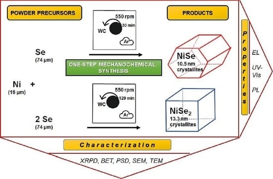
2. Materials and Methods
Mechanosynthesis of NiSe and NiSe
2 was performed in the planetary ball mill Pulverisette 6 (Fritsch, Idar-Oberstein, Germany) by the milling of nickel (98.8%, 16 μm, Penta Chemicals Ltd., Prague, Czech Republic) and selenium (99.5%, 74 μm, Aldrich, Darmstadt, Germany) powders according to these reactions:
The negative values of enthalpy change of the reactions (1) and (2) reported in Gmelin’s Handbook of Inorganic Chemistry for NiSe
1.
052 and NiSe
2 compounds support their thermodynamic feasibility [
17]. The milling conditions were as follows. The calculated amounts of Ni powder, 2.13 g and 1.36 g, and Se powder 2.87 g and 3.64 g with a total mass of 5 g for NiSe and NiSe
2 reactions, were homogenized before milling and put into a tungsten carbide milling chamber with a volume of 250 mL and 50 tungsten carbide balls with a diameter of 10 mm. Subsequently, the milling chamber was filled with an argon atmosphere. The rotation speed was 550 rpm, ball-to-powder ratio 73:1, and milling time from 5 to 120 min.
X-ray powder diffraction patterns (XRPD) of the milled samples were recorded on a Panalytical Empyrean diffractometer working in θ–2θ Bragg-Brentano geometry using a Cu
Kα1,2 X-ray source (0.154439 nm). For the incident beam path, 1/4° fixed divergence slit, 1/2° anti-scatter slit, the mask of 10 mm, and Soller slit (0.02 rad) were used. The diffractometer was equipped with a PIXcel3D detector. The phases were identified using the JCPDS PDF database. The data were analyzed utilizing the Fullprof suite software package [
18]. For the Rietveld refinement, the diffraction lines were modeled using the Thomas–Cox–Hastings function. During the refinement, lattice parameters, profile parameters, sample displacement, and background points were refined with atomic parameters kept fixed.
The specific surface area measurements were performed on a Gemini 2360 sorption apparatus (Micromeritics, Norcross, GA, USA) by the low-temperature nitrogen adsorption method.
The particle size analyzer Mastersizer 2000E with a laser diffraction system (Malvern Pananalytical, Malvern, UK), a dry feeder Scirocco 2000M, and the measuring range 0.02–2000 μm were used for the particle size distributions (PSD) measurements.
Scanning electron microscopy (SEM) observations were done with the microscope MIRA3 FE-SEM (TESCAN, Brno, Czech Republic), including an EDX detector (Oxford Instrument, Oxford, UK) for the energy dispersive X-ray analysis (EDX) of the observed samples.
A transmission electron microscopy (TEM) study was performed using a JEOL 2100F UHR microscope operated at 200 kV with a Schottky field emission source. The high-resolution mode was used for taking the images, and the selected area electron diffraction (SAED) was used for the structure identification. Regarding SAED experiments, the microscope was precisely calibrated using MoO3 crystal. Gold nanoparticles were used for double-checking, as well. The studied samples were dispersed in absolute ethanol and ultrasonicated for 10 min before observation to reduce the agglomeration of the crystals. These sample dispersions were placed on a copper support grid covered with ultra-thin flat carbon film and stored in a vacuum.
A standard four-point probe technique was used to study the electrical properties of the samples [
19,
20]. The samples in the form of pellets were pressed from 0.41 g of NiSe and NiSe
2 powder products under the pressure of 3 t, without retention time, and at room temperature, in a laboratory hydraulic press (Specac, Fort Washington, PA, USA). The four-point test head (Ossila Ltd., Sheffield, UK) was placed on the measured pellet and fixed to its geometrical center during the measurements with a source-measure unit as reported in our previous work [
16]. The probe tips were fixed at the same position and loaded with a constant contact force to obtain reproducible results. The distance between the probe tips was 1.27 mm. The diameter of the circular NiSe and NiSe
2 pellets was 7.06 ± 0.01 mm, and their average room temperature densities of 7.2 and 6.88 g.cm
−3 were taken from the commonly available literature.
The UV–Vis spectrophotometer Helios Gamma (Thermo Electron Corporation, Warwickshire, UK) was used to measure the optical absorption spectra of the samples. The studied samples were dispersed in absolute ethanol by ultrasonic stirring and poured into the quartz cell.
A photon-counting spectrofluorometer PC1 (ISS, San Antonio, TX, USA) recorded photoluminescence spectra (PL) of the samples at room temperature and with a photoexcitation wavelength of 360 nm. The excitation source was a 300 W xenon lamp, and the widths of the excitation and emission slits were set to 0.5 and 1 mm. The studied samples were dispersed in absolute ethanol by ultrasonic stirring and placed into the quartz cell cuvette for spectral analysis.
3. Results and Discussion
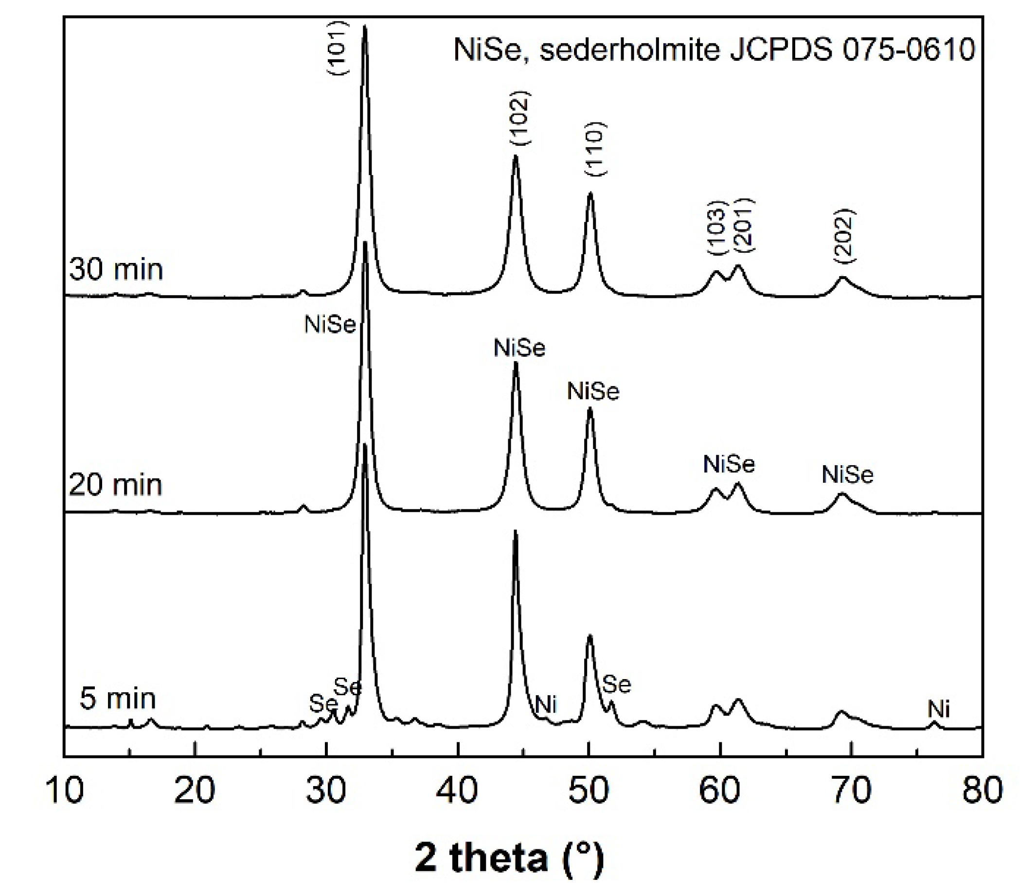
The results of XRPD indicate that the mechanochemical reaction of Ni with Se according to Equation (1), starts with the formation of the NiSe phase (JCPDS 075-0610), which is already present in the system after 5 min of milling (see
Figure 1). After the additional 15 min of milling, the product mainly shows the diffraction peaks belonging to the hexagonal NiSe (sederholmite,
P6
3/
mmc space group) with cell parameters
a = 3.66 Å nm,
c = 5.33 Å. Only traces of unreacted elemental nickel metal (JCPDS 004-0850) were detected. Moreover, a weak reflection at 16.5° 2θ might be assigned to the monoclinic wilkmanite Ni
3Se
4 phase (JCPDS 018-0890,
I2/
m space group), which would be in accordance with the observation of unreacted nickel metal. After 30 min of milling, the weight ratio of the NiSe/Ni
3Se
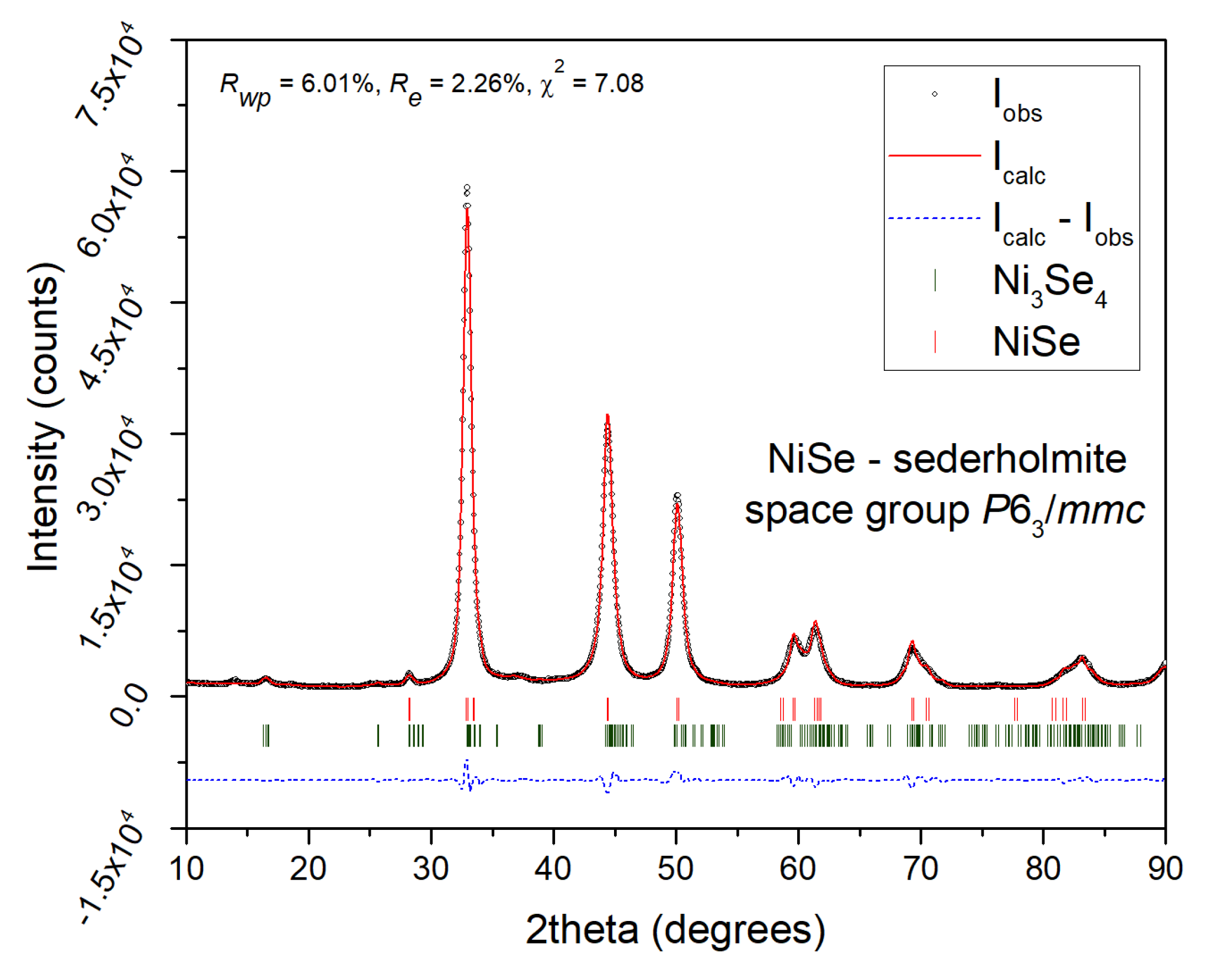
4 phases was determined to be approximately 90/10. The graphical output of the Rietveld refinement in
Figure 2 proved that the refined lattice parameters of the NiSe phase are as follows:
a =
b = 3.6278(2) Å,
c = 5.3318(4) Å. The average NiSe crystallite size of 10.5 nm was calculated using the Scherrer formula corrected for instrumental broadening. For the calculation, the integral breadth of (101), (102), (110), and (103) crystallographic planes were used. The provided value is rather informative due to a strong overlap of reflections, high FWHM values, and admixture formation.
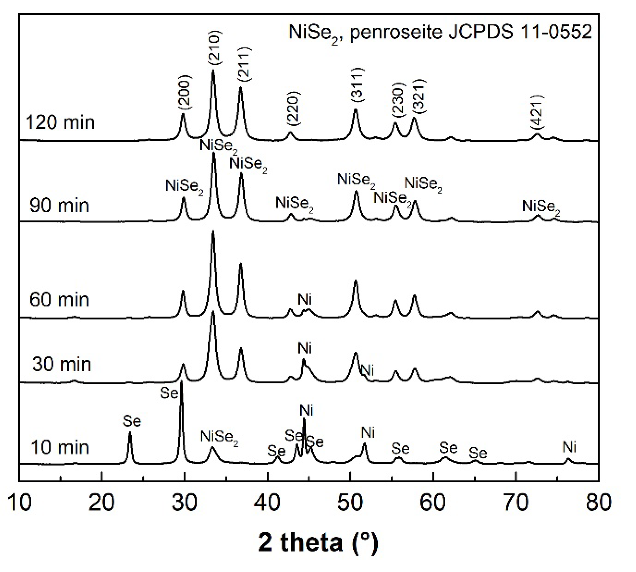
The XRPD patterns depicted in
Figure 3 confirm the start of the mechanochemical reaction of Ni with 2 Se according to Equation (2) with the formation of the NiSe
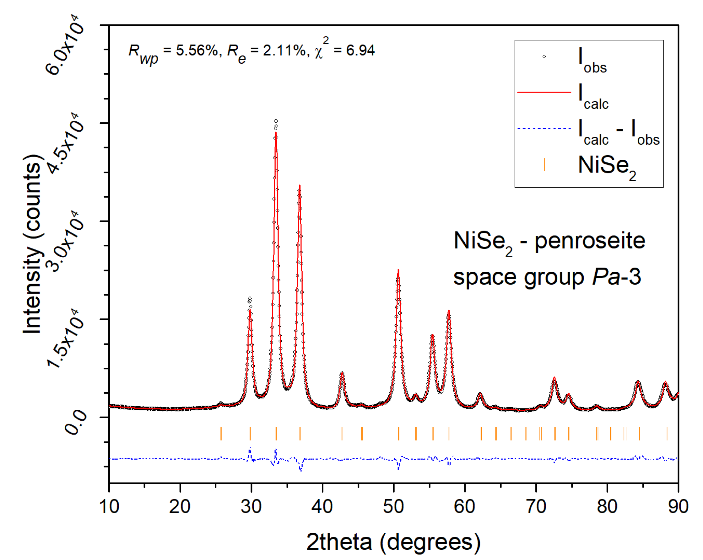
2 (JCPDS 011-0552) already after 10 min of milling as well as for NiSe mechanochemical synthesis, following the more negative formation enthalpy compared to the hexagonal NiSe phase. However, the unreacted nickel (JCPDS 004-0850) and selenium (JCPDS 073-0465) peaks clearly predominate. After 90 min of milling, the penroseite NiSe
2 phase with the cubic structure (
Pa-3 space group) and the cell parameter
a = 5.9604 Å as the major product crystallizes. Only traces of unreacted nickel are present in the pattern. The Rietveld refinement of the XRPD data of the 120 min sample (
Figure 4) confirmed NiSe
2 phase purity with the refined crystal lattice parameter
a = 5.960 Å, and the average size of crystallites 13.3 nm.
The phase structure, composition, and morphology of mechanochemically synthesized NiSe and NiSe2 can affect the physical and chemical properties of such uniquely prepared materials.
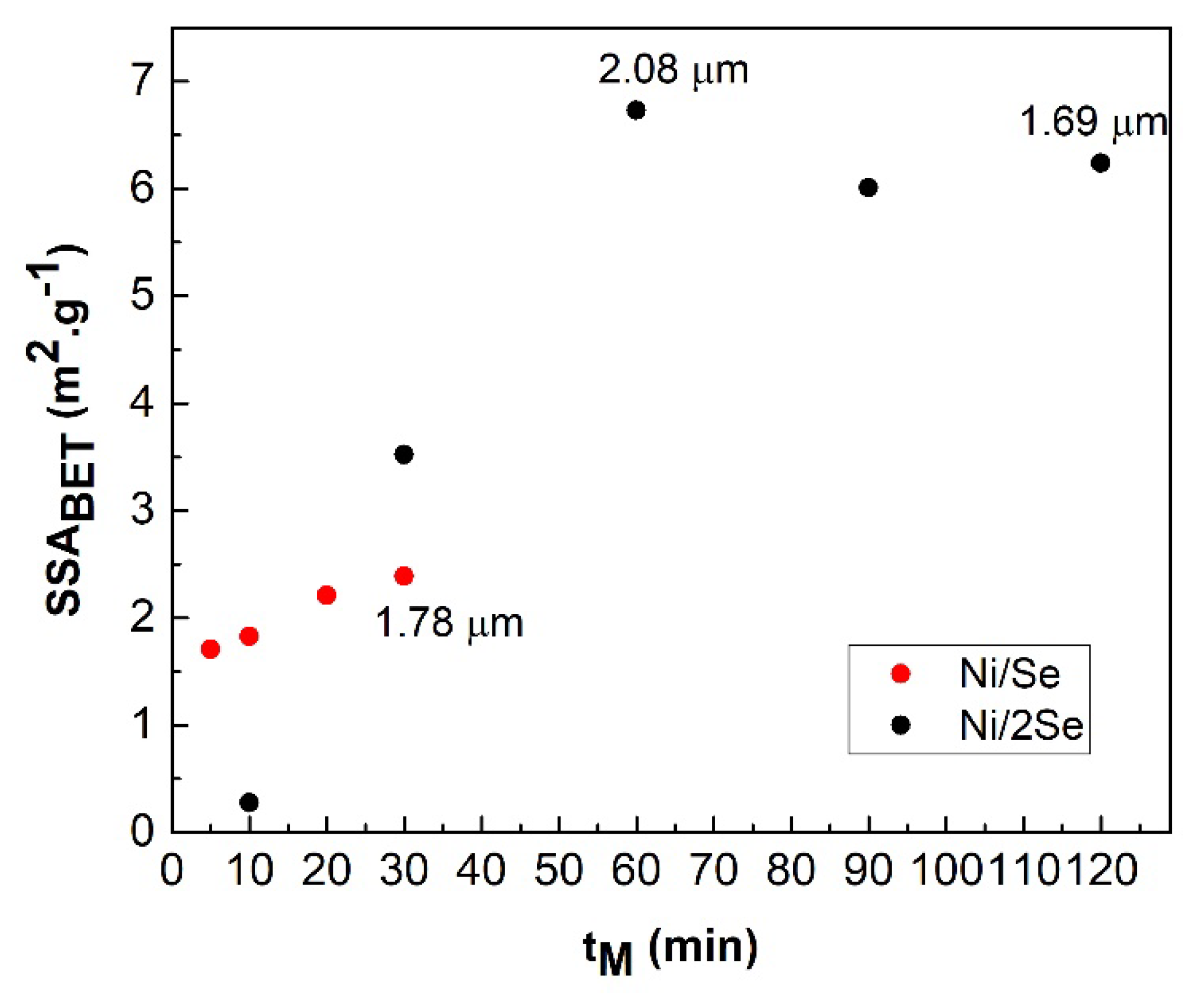
From the dependences in
Figure 5, it follows that the specific surface area, SSA
BET of both Ni/Se and Ni/2Se samples increases with the time of milling. The maximum value of 2.39 m
2.g
−1 for the Ni/Se sample milled for 30 min indicates the completion of the mechanochemical reaction with the formation of the NiSe phase, while the sample Ni/2Se reaches the maximum SSA
BET value of 6.73 m
2.g
−1 after 60 min of milling. Subsequently, the mean particle size of this sample decreases from 2.08 to 1.69 μm with increasing milling time, but due to the mutual agglomeration of the particles of the NiSe
2 product, the specific surface area decreases. It is known from the literature that the maximum value of SS
A is reached at the end of the mechanochemical reaction for TMCs, but this does not correspond to the case of NiSe
2 [
15,
21,
22].
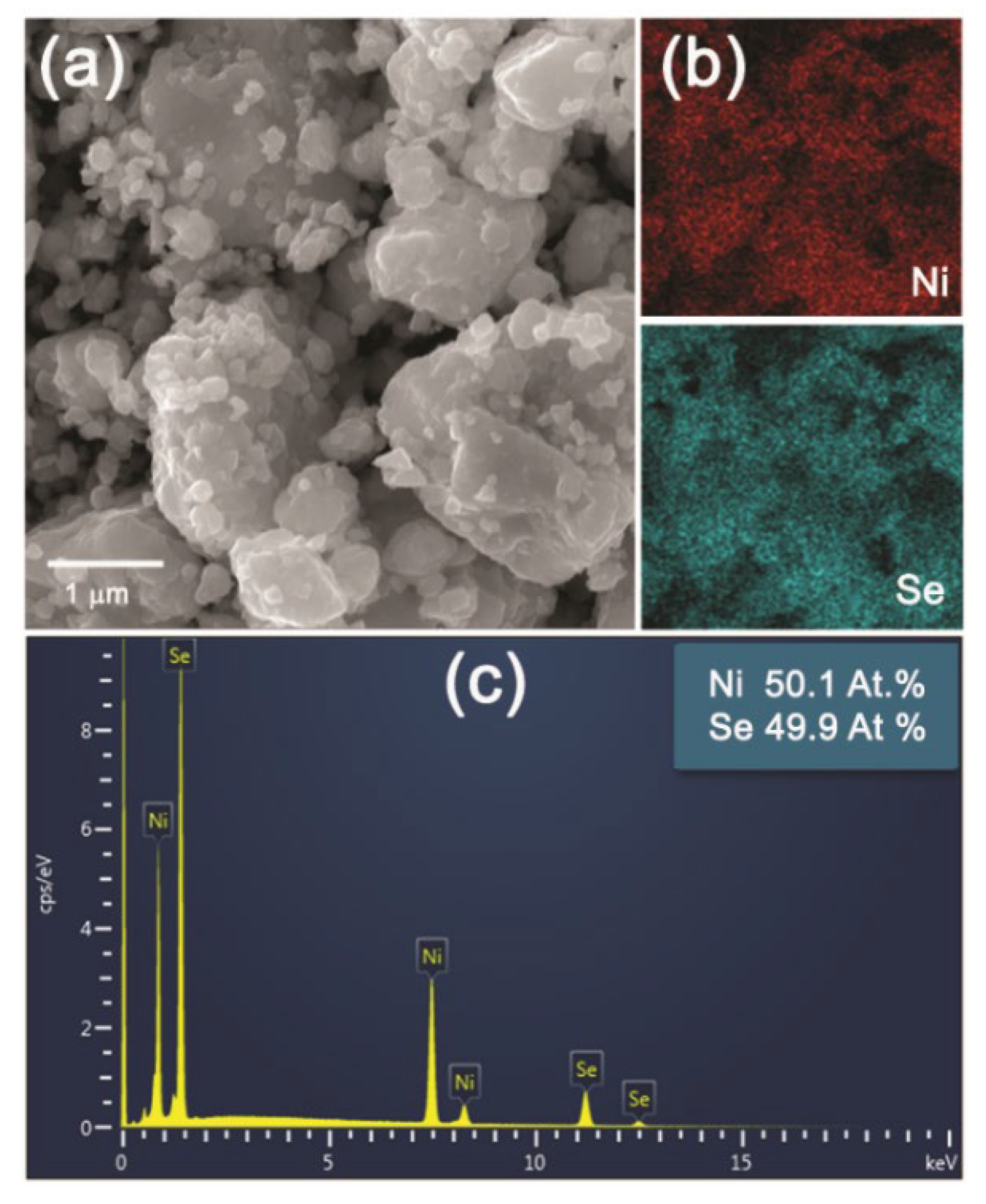
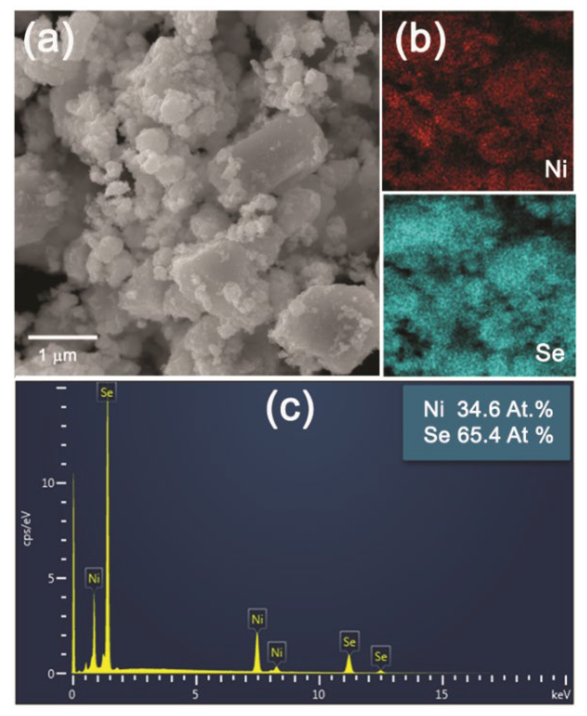
Lower magnification SEM images of the NiSe and NiSe
2 products in
Figure 6a and
Figure 7a demonstrated the similar agglomerated grains having an irregular shape with inhomogeneous size distribution. The mapping of Ni and Se elements evidenced their homogeneous distribution in both products (
Figure 6b and
Figure 7b). The quantitative EDX analyses in
Figure 6c and
Figure 7c confirmed close to the stoichiometric chemical composition of both nickel selenides with atomic ratios of almost 1:1 and 1:2 for NiSe and NiSe
2. A certain deviation in the determination of the elemental composition of the products can probably be caused by their surface which is not entirely flat. The crystallinity and the crystallite size of the products were also examined in more detail by TEM analysis.
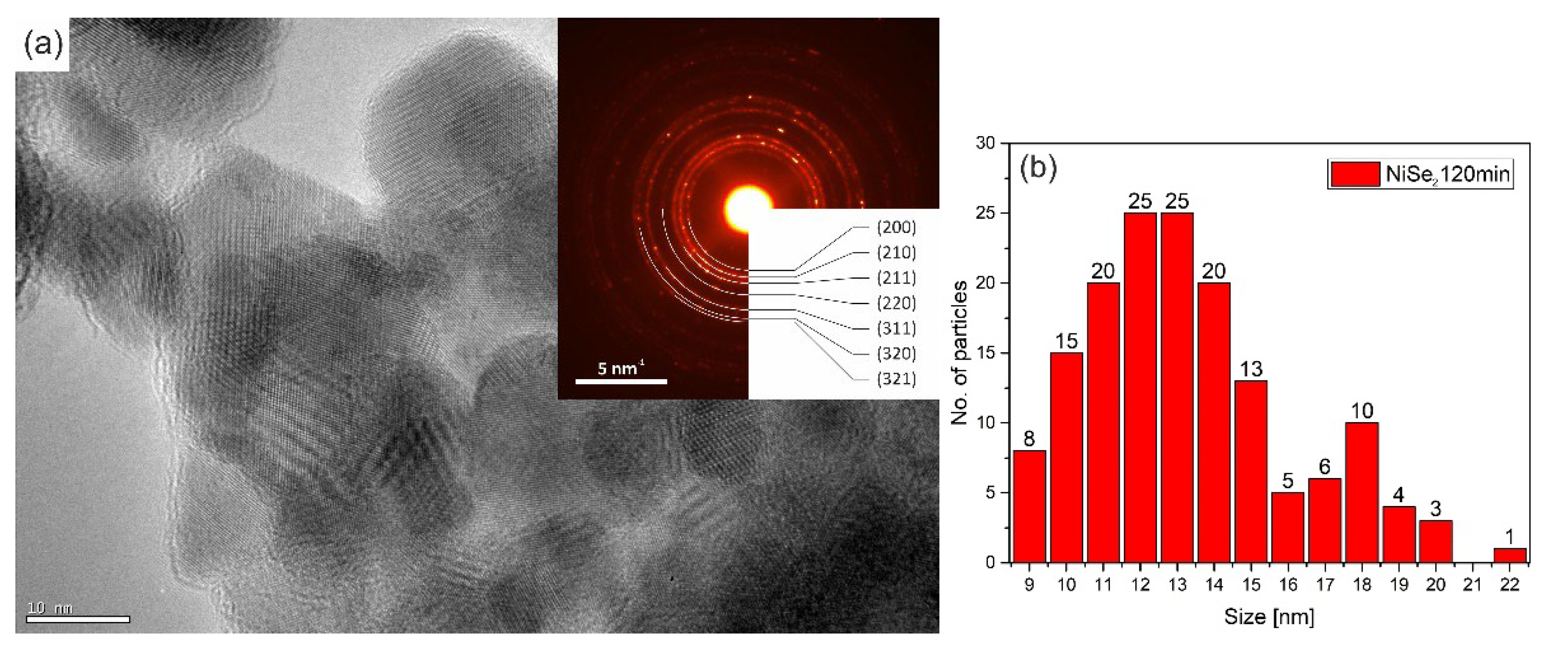
The crystallite size of the NiSe and NiSe
2 samples was calculated based on several images taken in bright field STEM mode to avoid the unwanted diffraction effect. More than 50 crystallites were included in the statistics for each sample.
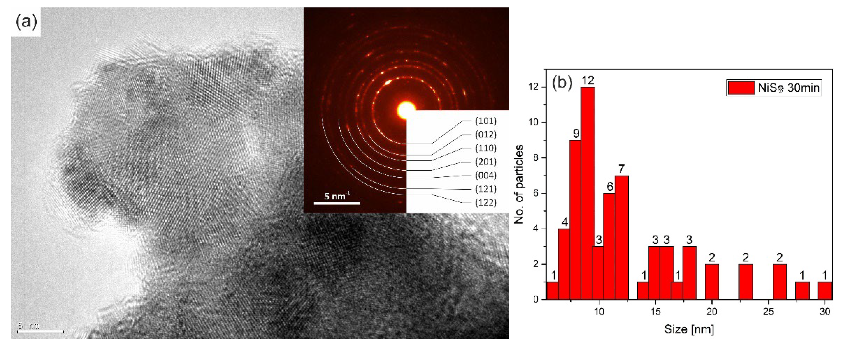
Figure 8b showed the result of the statistics for the sample NiSe in the form of a skewed right histogram. The crystallite size in interval 7–12 nm was observed with the highest frequency.
Figure 8a illustrates the agglomerates of crystallites in which some displayed atomic layers. The embedded diffraction pattern confirmed NiSe hexagonal phase with space group
P6
3/
mmc (194). The calculated average crystallite size of sample NiSe
2 was in the interval of 10–15 nm (
Figure 9b), which is a bit more than for sample NiSe. The crystallites of the NiSe
2 sample are visualized in
Figure 9a as agglomerated particles. Most of them have distinguishable atomic planes. Analysis of diffraction pattern proved the cubic NiSe
2 phase with space group
Pa-3 (205). Analyses of selected area electron diffraction are consistent with XRPD results. When comparing the two TEM images
Figure 8a and
Figure 9a, it should be taken into account that the images were not acquired at the same magnification.
As data on the electrical properties of nickel selenides are very rare in the literature, the electrical conductivity, resistivity, and sheet resistance values of mechanochemically synthesized NiSe and NiSe
2 were investigated and measured.
Table 1 shows the resulting values of individual electrical quantities coming from 200 measured values for each product.
The conductivity of NiSe
2 is slightly higher than that of NiSe, which is related to the larger crystallite size of NiSe
2 (10–15 nm). This crystallite and/or grain size effect is even more evident at the resistivity value, which is significantly lower for NiSe
2 than for NiSe (7–12 nm). The electrical resistivity values at room temperature are of the same order as the values reported for nickel selenide prepared by chemical deposition [
23], and the solid-state reaction method [
24]. The descriptive statistics were performed from the values measured on 20 samples. High standard deviations for the NiSe sample indicate a problem with reproducing the electrical properties of the sample prepared by mechanochemical synthesis. We note that separate statistics for individual samples provide the expected standard deviation, however with significant variation in their mean values.
Nickel selenides are classified as p-type semiconductors, and their bandgap energy value is 620 nm (2.0 eV). According to the literature, the bandgaps of NiSe and NiSe
2 are narrower than that of nickel oxide (3.6–4.0 eV) and wider than bulk nickel sulphide (0.4 eV). Therefore, they also become potential candidates for solar cells [
10].
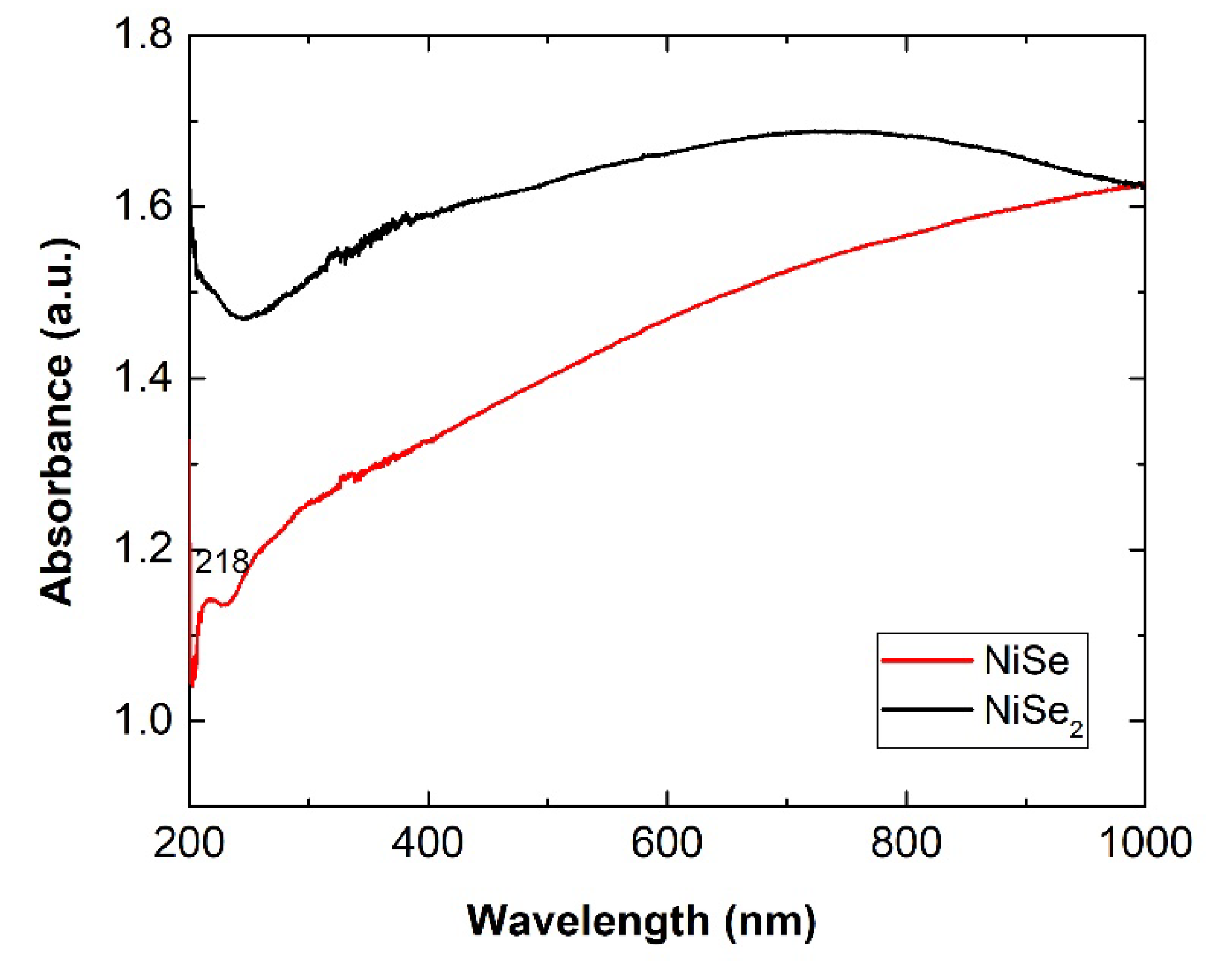
Figure 10 shows the measured UV–Vis optical absorption spectra of both mechanochemically synthesized nickel mono- and diselenides. Both nickel selenides absorbed UV–Vis radiation in the entire range from 200 to 1000 nm, which fits well when using the solar spectrum. The slightly smaller particles and nanocrystallites of NiSe likely caused the weak excitonic peak at 218 nm (5.65 eV).
For NiSe
2, no excitonic peak was observed in the spectrum. The linear part of the Tauc plots in
Figure 11 indicates that the NiSe and NiSe
2 semiconductors involve a direct optical transition. The bandgaps 1.35 eV for NiSe and 1.9 eV for NiSe
2 were determined by extrapolating the linear regions of the plots to (αhν)
2 = 0. The bandgap value of NiSe is red-shifted compared to the value of bulk NiSe as well as the value of 1.61 eV for NiSe thin films prepared by chemical deposition and reported by Hankare and co-authors [
23]. The determined value of NiSe
2 bandgap energy more or less corresponds to the bandgap of bulk nickel selenide (2.0 eV).
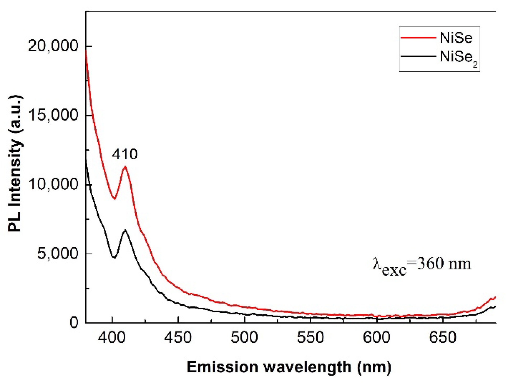
The room temperature PL emission spectra of nickel selenides are shown in
Figure 12. Light with a wavelength of 360 nm and corresponding to a photon energy of 3.42 eV was used for irradiation—photoexcitation of the samples. This photon energy is absorbed to excite the transition of electrons from the valence band to the conduction band.
Regarding the peak position, the situation is similar in both samples. The samples have a broad violet emission around 410 nm (3 eV). However, the emission peak of the NiSe
2 sample has a slightly lower luminescence intensity than NiSe one. Since the emission of PL radiation is mainly due to the recombination of photo-excited electrons and holes, the lower PL intensity could indicate a lower rate of electron/holes recombination in NiSe
2. Our results are in accordance with previously published papers [
1,
8,
25]. The emission peak situated at 410 nm may be attributed to the defects. These defects occurring in the nanocrystals are generated as a result of high-energy milling. Nevertheless, both samples exhibit only weak photoluminescence.
Table 2 summarizes literature data on NiSe and NiSe
2 synthesized by various techniques, including mechanochemical synthesis. By comparing the energy and time requirements of individual preparation methods, mechanosynthesis in the planetary mill is a fast, one step, and takes place at ambient temperature. In addition, it does not require solvents, additional reagents, or subsequent operations such as washing and drying the product. The crystallite sizes of NiSe and NiSe
2 prepared by our procedure reach low values, which could enable their possible applications listed in
Table 2 for nickel selenides synthesized by other conventional methods. However, verification and further research are needed.


 ,
, 

