
Conductive Inks Based on Melamine Intercalated Graphene Nanosheets for Inkjet Printed Flexible Electronics


 , ,
, ,
Abstract
:
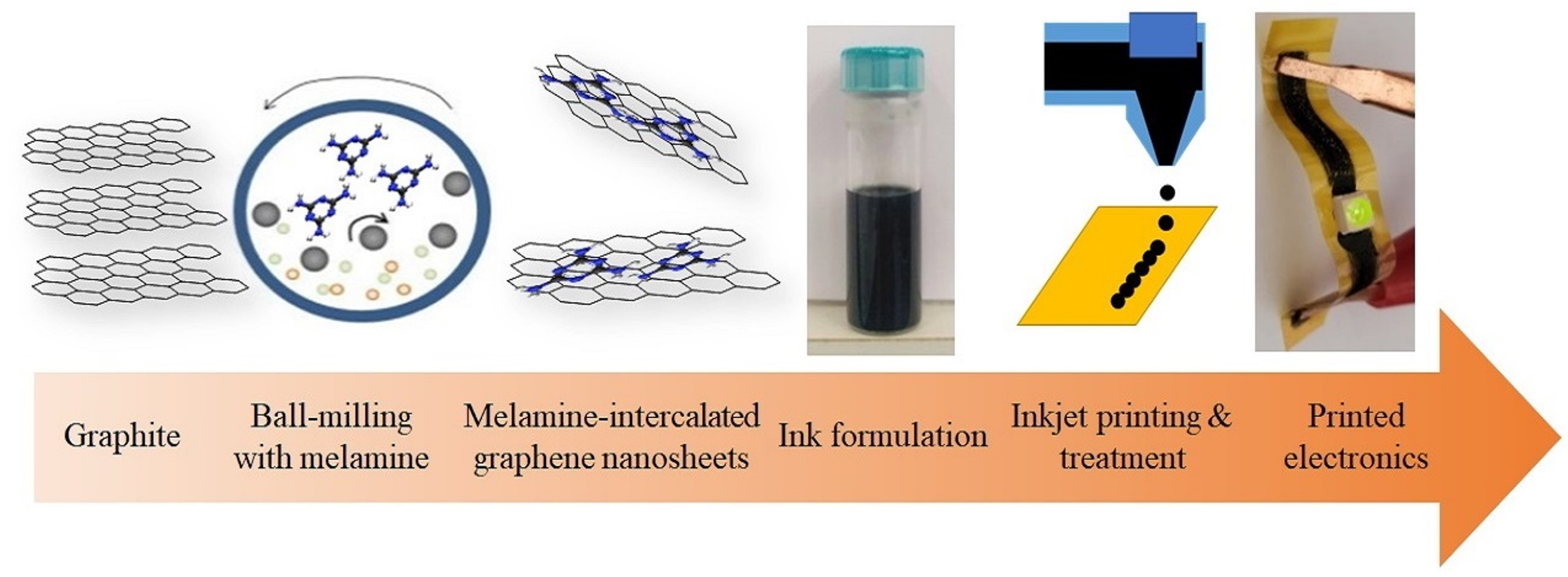
1. Introduction
2. Materials and Methods
2.1. Materials
2.2. Mechanochemical Synthesis of Melamine-Intercalated Graphene Nanosheets (M-GNS)
2.3. Preparation of M-GNS Inks
2.4. Inkjet Printing of M-GNS Inks and Post-Printing Processing
2.5. Characterization
3. Results and Discussion
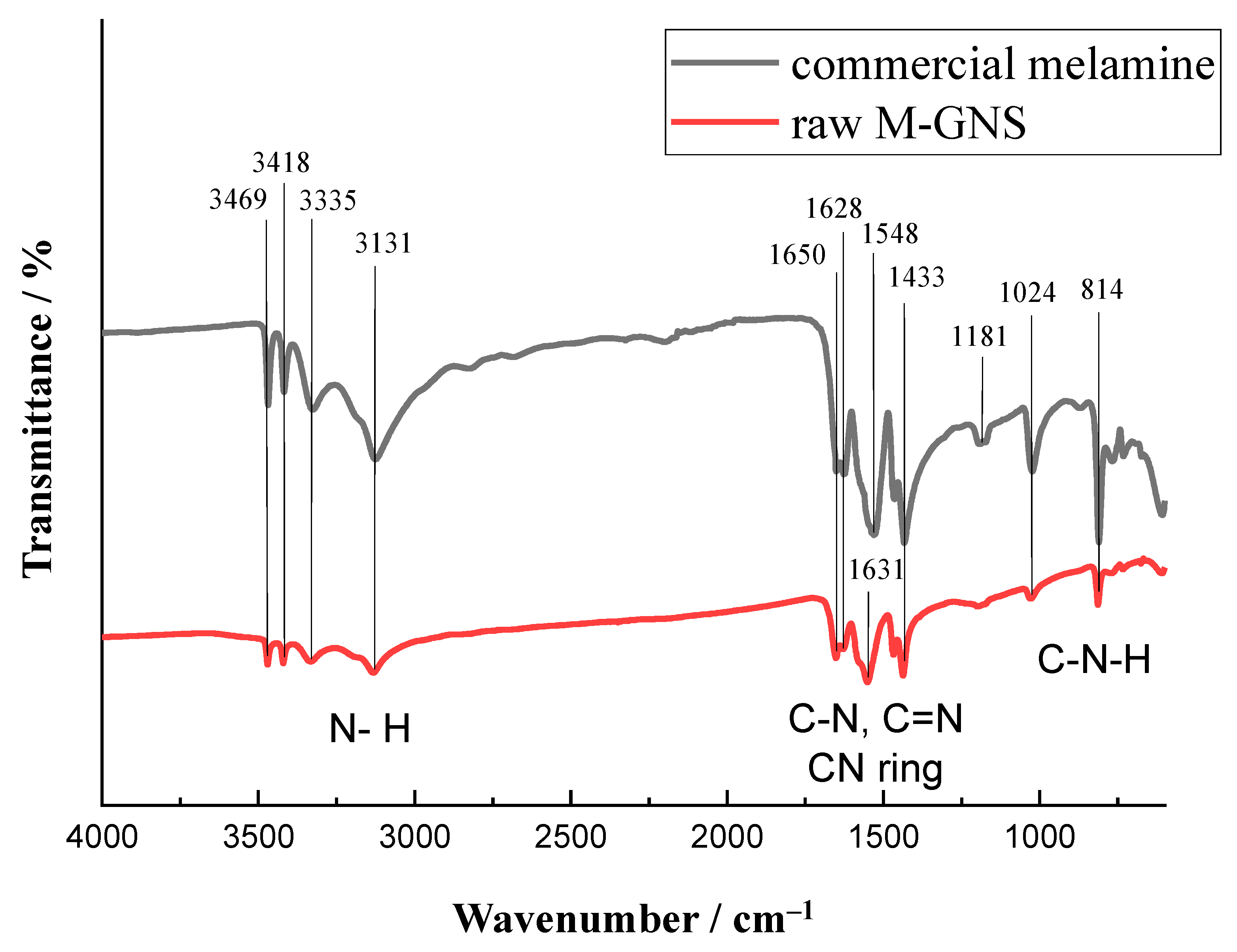
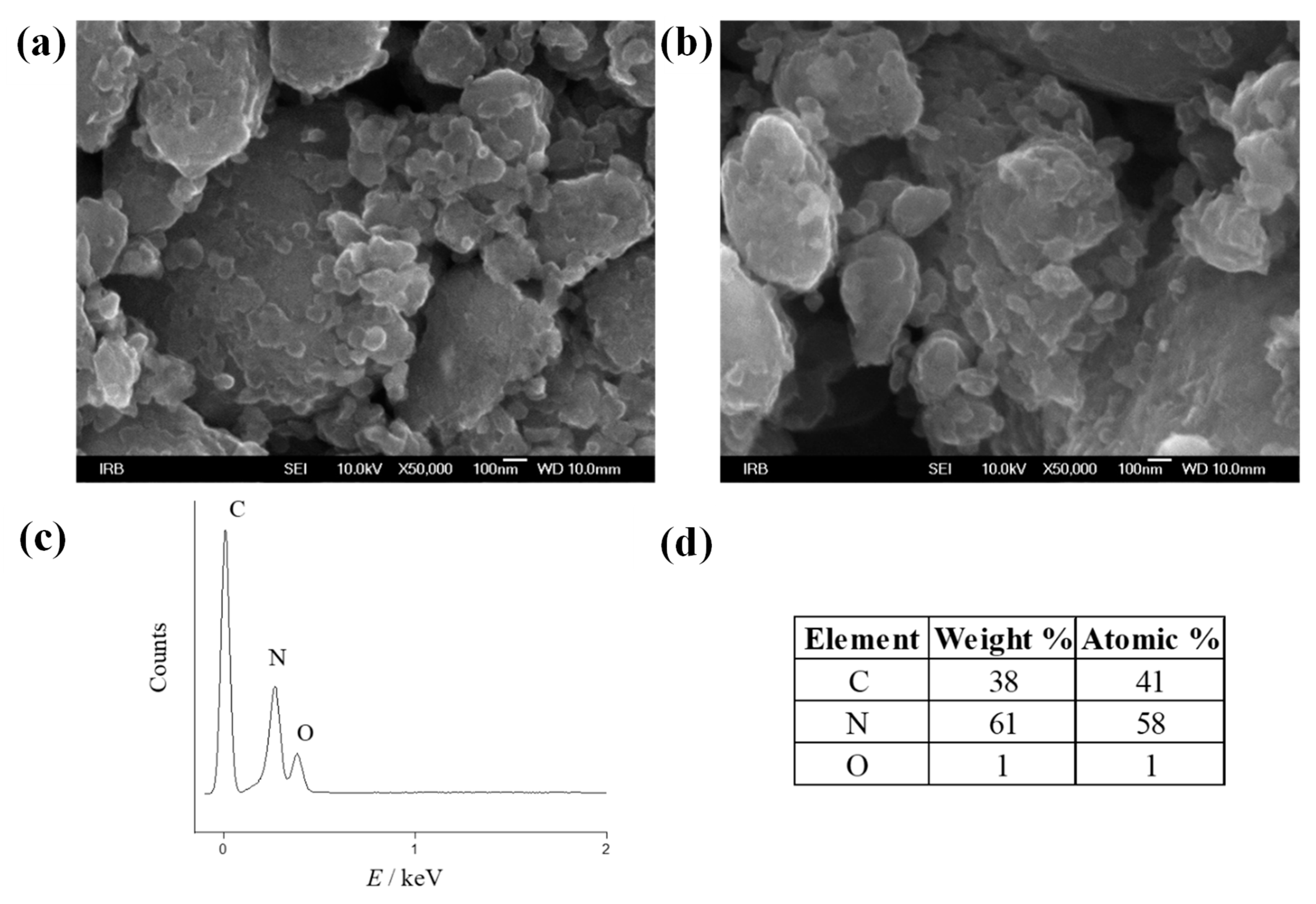
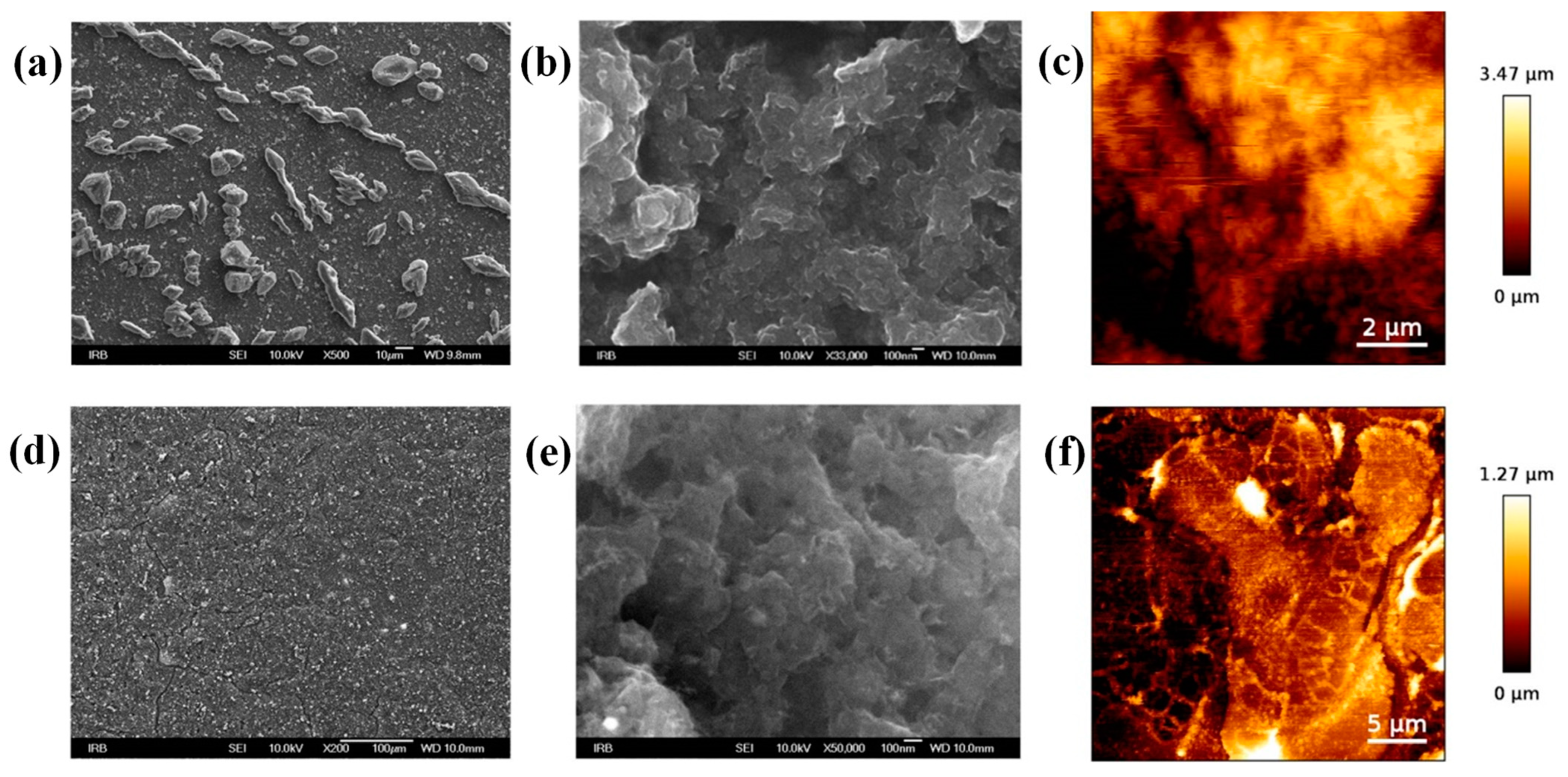
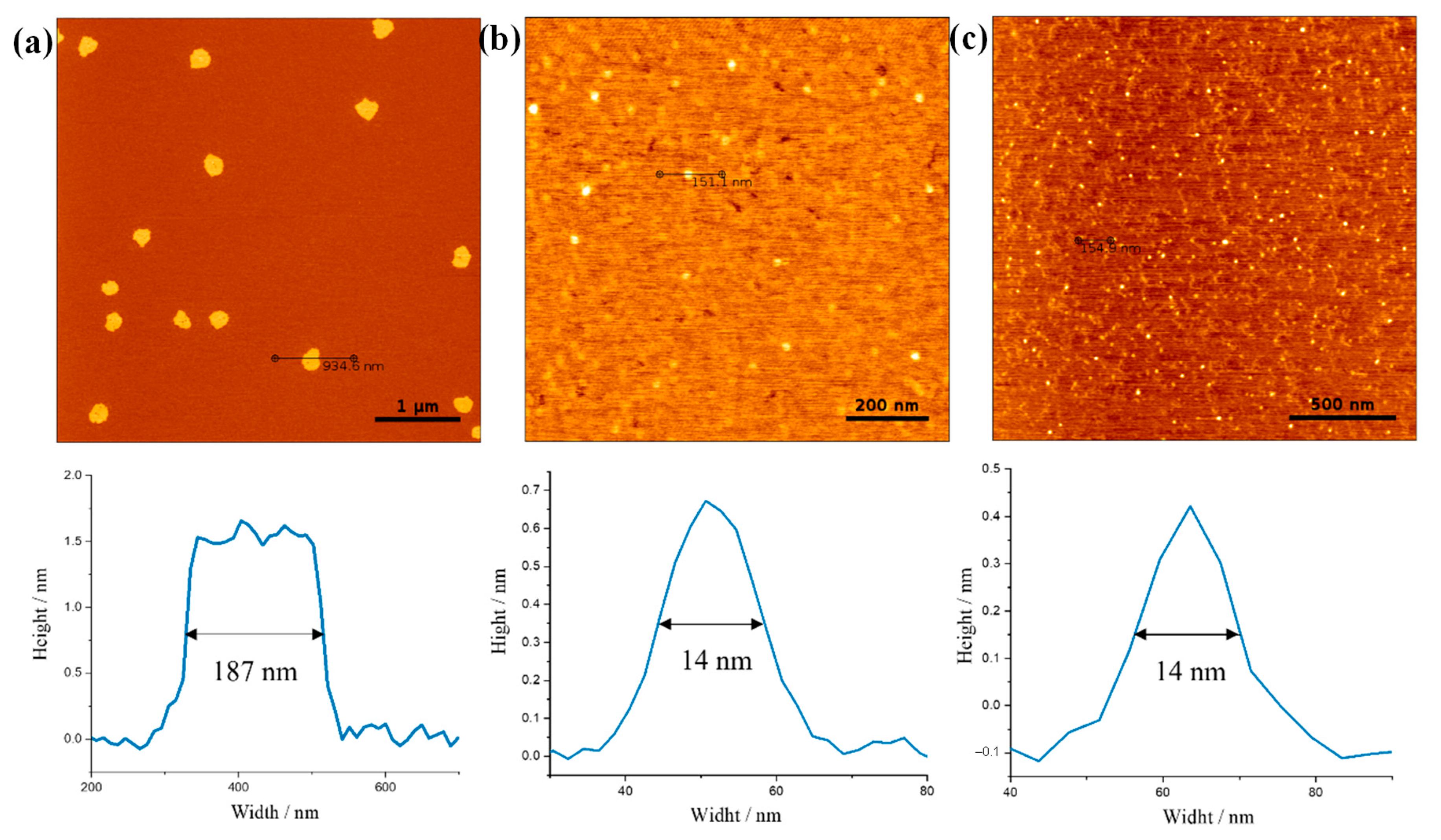
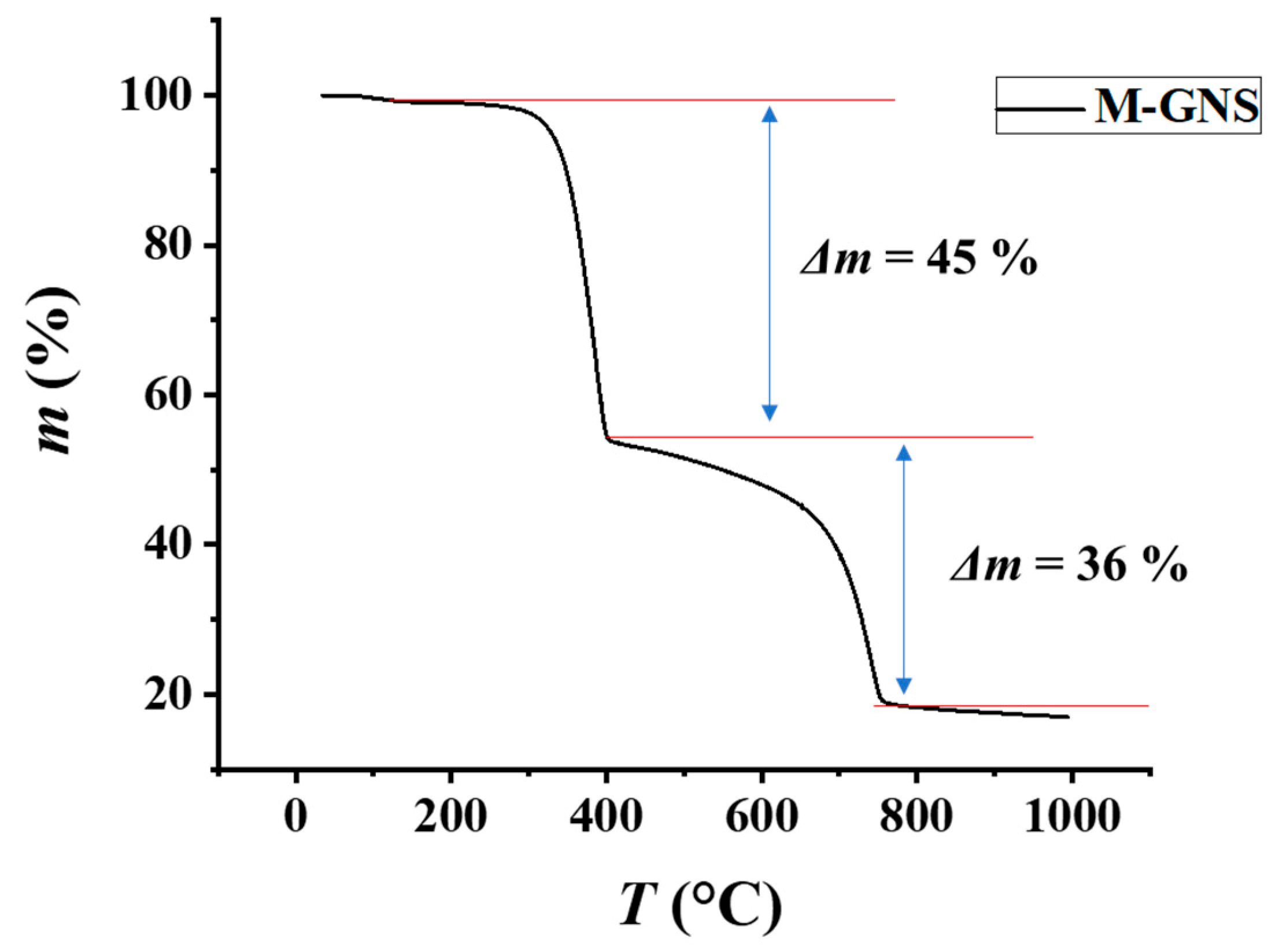
3.1. Synthesis and Characterization of Melamine-Intercalated Graphene Nanosheets
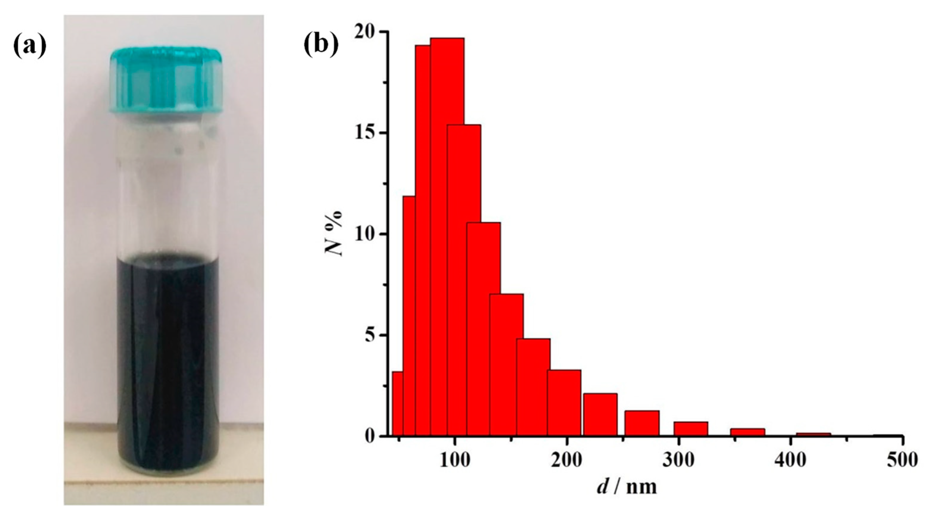
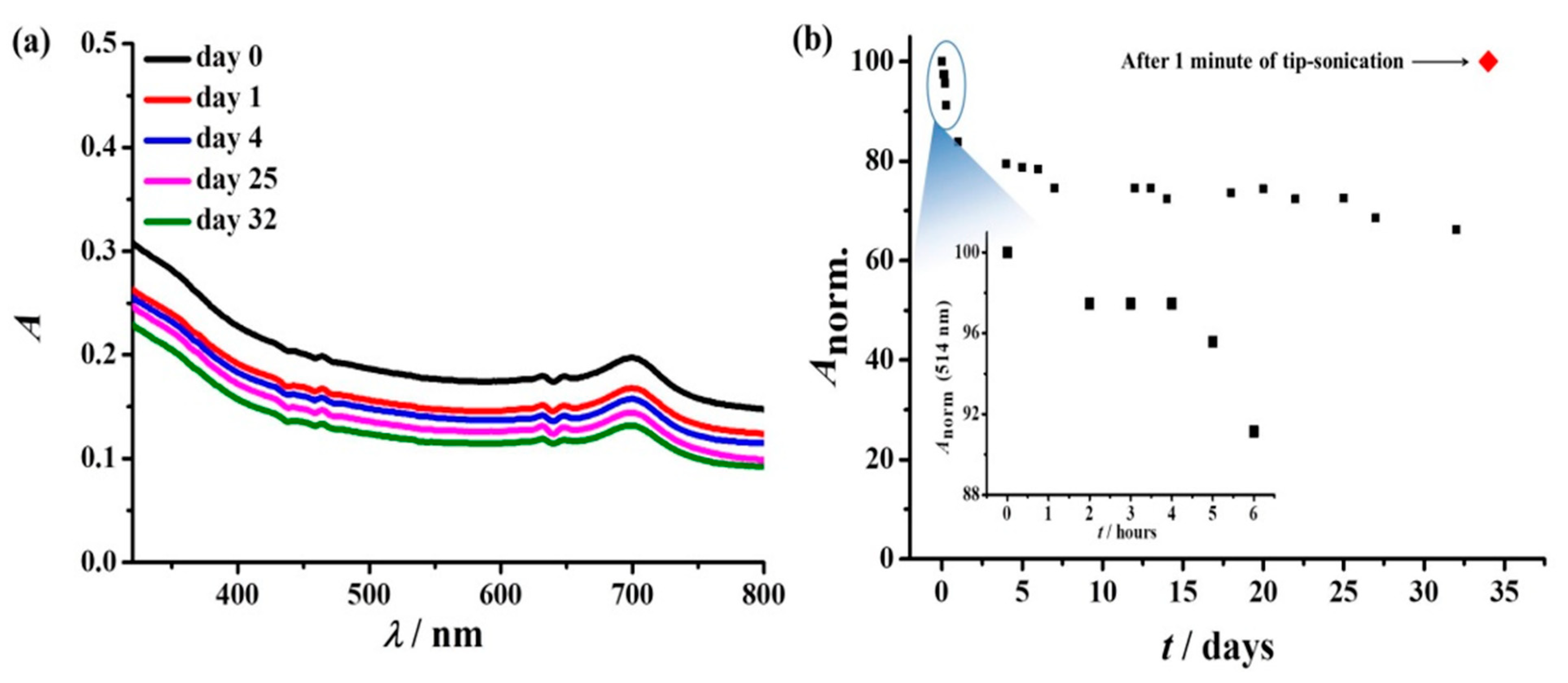
3.2. Preparation and Characterization of M-GNS Inks
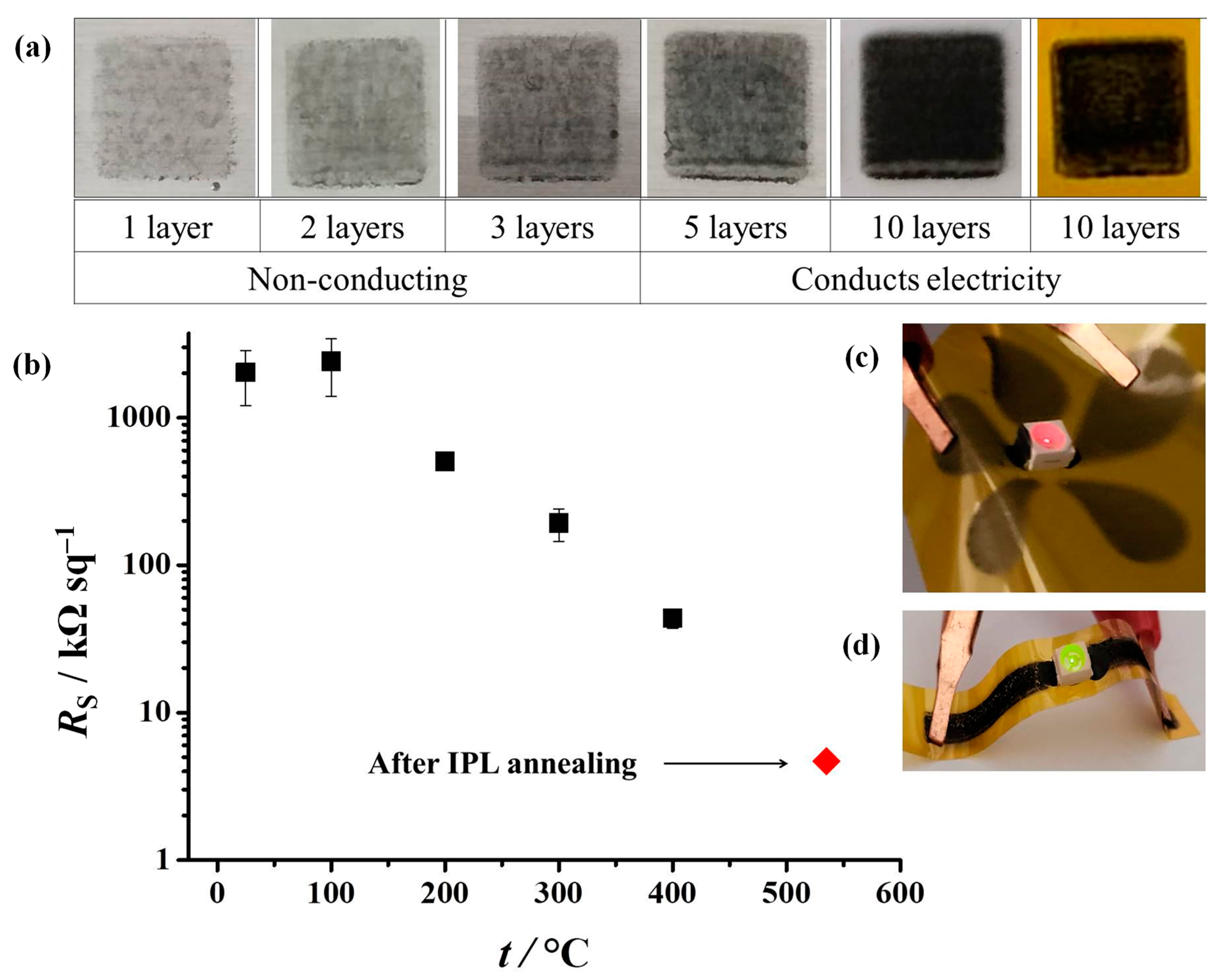
3.3. Inkjet Printing and Post-Printing Processing
4. Conclusions
Supplementary Materials
Author Contributions
Funding
Institutional Review Board Statement
Informed Consent Statement
Data Availability Statement
Acknowledgments
Conflicts of Interest
References
- Raut, N.C.; Al-Shamery, K. Inkjet printing metals on flexible materials for plastic and paper electronics. J. Mater. Chem. C 2018, 6, 1618–1641. [Google Scholar] [CrossRef]
- Nayak, L.; Mohanty, S.; Nayak, S.K.; Ramadoss, A. A review on inkjet printing of nanoparticle inks for flexible electronics. J. Mater. Chem. C 2019, 7, 8771–8795. [Google Scholar] [CrossRef]
- Wu, W. Inorganic nanomaterials for printed electronics: A review. Nanoscale 2017, 9, 7342–7372. [Google Scholar] [CrossRef] [PubMed]
- Khan, Y.; Thielens, A.; Muin, S.; Ting, J.; Baumbauer, C.; Arias, A.C. A New Frontier of Printed Electronics: Flexible Hybrid Electronics. Adv. Mater. 2020, 32, 1905279. [Google Scholar] [CrossRef]
- Huang, L.; Huang, Y.; Liang, J.; Wan, X.; Chen, Y. Graphene-based conducting inks for direct inkjet printing of flexible conductive patterns and their applications in electric circuits and chemical sensors. Nano Res. 2011, 4, 675–684. [Google Scholar] [CrossRef]
- Pietsch, M.; Schlisske, S.; Held, M.; Strobel, N.; Wieczorek, A.; Hernandez-Sosa, G. Biodegradable inkjet-printed electrochromic display for sustainable short-lifecycle electronics. J. Mater. Chem. C 2020, 8, 16716–16724. [Google Scholar] [CrossRef]
- Ali, Z.; Perret, E.; Barbot, N.; Siragusa, R.; Hely, D.; Bernier, M.; Garet, F. Authentication Using Metallic Inkjet-Printed Chipless RFID Tags. IEEE Trans. Antennas Propag. 2020, 68, 4137–4142. [Google Scholar] [CrossRef]
- Baby, T.T.; Rommel, M.; von Seggern, F.; Friederich, P.; Reitz, C.; Dehm, S.; Kübel, C.; Wenzel, W.; Hahn, H.; Dasgupta, S. Sub-50 nm Channel Vertical Field-Effect Transistors using Conventional Ink-Jet Printing. Adv. Mater. 2017, 29, 1603858. [Google Scholar] [CrossRef]
- Ivanisevic, I.; Milardović, S.; Ressler, A.; Kassal, P. Fabrication of an All-Solid-State Ammonium Paper Electrode Using a Graphite-Polyvinyl Butyral Transducer Layer. Chemosensors 2021, 9, 333. [Google Scholar] [CrossRef]
- Cummins, G.; Desmulliez, M.P.Y. Inkjet printing of conductive materials: A review. Circuit World 2012, 38, 193–213. [Google Scholar] [CrossRef]
- Derby, B. Inkjet Printing of Functional and Structural Materials: Fluid Property Requirements, Feature Stability, and Resolution. Ann. Rev. Mater. Res. 2010, 40, 395–414. [Google Scholar] [CrossRef]
- Kamyshny, A.; Magdassi, S. Conductive nanomaterials for 2D and 3D printed flexible electronics. Chem. Soc. Rev. 2019, 48, 1712–1740. [Google Scholar] [CrossRef] [PubMed]
- Kamyshny, A.; Magdassi, S. Conductive Nanomaterials for Printed Electronics. Small 2014, 10, 3515–3535. [Google Scholar] [CrossRef] [PubMed]
- Zea, M.; Moya, A.; Fritsch, M.; Ramon, E.; Villa, R.; Gabriel, G. Enhanced Performance Stability of Iridium Oxide-Based pH Sensors Fabricated on Rough Inkjet-Printed Platinum. Acs Appl. Mater. Interfaces 2019, 11, 15160–15169. [Google Scholar] [CrossRef] [PubMed]
- Sjoberg, P.; Määttänen, A.; Vanamo, U.; Novell, M.; Ihalainen, P.; Andrade, F.J.; Bobacka, J.; Peltonen, J. Paper-based potentiometric ion sensors constructed on ink-jet printed gold electrodes. Sens. Actuators B-Chem. 2016, 224, 325–332. [Google Scholar] [CrossRef]
- Milardovic, S.; Ivanišević, I.; Rogina, A.; Kassal, P. Synthesis and Electrochemical Characterization of AgNP Ink Suitable for Inkjet Printing. Int. J. Electrochem. Sci. 2018, 13, 11136–11149. [Google Scholar] [CrossRef]
- Park, J.; Yoon, H.; Kim, G.; Lee, B.; Lee, S.; Jeong, S.; Kim, T.; Seo, J.; Chung, S.; Hong, Y. Highly Customizable All Solution-Processed Polymer Light Emitting Diodes with Inkjet Printed Ag and Transfer Printed Conductive Polymer Electrodes. Adv. Funct. Mater. 2019, 29, 1902412. [Google Scholar] [CrossRef]
- Kulkarni, M.V.; Apte, S.K.; Naik, S.D.; Ambekar, J.; Kale, B. Ink-jet printed conducting polyaniline based flexible humidity sensor. Sens. Actuators B-Chem. 2013, 178, 140–143. [Google Scholar] [CrossRef]
- Gbaguidi, A.; Madiyar, F.; Kim, D.; Namilae, S. Multifunctional inkjet printed sensors for MMOD impact detection. Smart Mater. Struct. 2020, 29, 085052. [Google Scholar] [CrossRef]
- Tortorich, R.P.; Song, E.; Choi, J.W. Inkjet-Printed Carbon Nanotube Electrodes with Low Sheet Resistance for Electrochemical Sensor Applications. J. Electrochem. Soc. 2014, 161, B3044–B3048. [Google Scholar] [CrossRef]
- Vasiljevic, D.Z.; Mansouri, A.; Anzi, L.; Sordan, R.; Stojanovic, G.M. Performance Analysis of Flexible Ink-Jet Printed Humidity Sensors Based on Graphene Oxide. IEEE Sens. J. 2018, 18, 4378–4383. [Google Scholar] [CrossRef]
- Huang, Q.J.; Zhu, Y. Printing Conductive Nanomaterials for Flexible and Stretchable Electronics: A Review of Materials, Processes, and Applications. Adv. Mater. Technol. 2019, 4, 1800546. [Google Scholar] [CrossRef]
- Htwe, Y.Z.N.; Mariatti, M. Printed graphene and hybrid conductive inks for flexible, stretchable, and wearable electronics: Progress, opportunities, and challenges. J. Sci. Adv. Mater. Devices 2022, 7, 100435. [Google Scholar] [CrossRef]
- Htwe, Y.Z.N.; Mariatti, M. Surfactant-assisted water-based graphene conductive inks for flexible electronic applications. J. Taiwan Inst. Chem. Eng. 2021, 125, 402–412. [Google Scholar] [CrossRef]
- Maribou, K.; Gil, W.; Al Ghaferi, A.; Saadat, I.; Alhammadi, K.; Khair, A.M.; Younes, H. Assessing the Stability of Inkjet-Printed Carbon Nanotube for Brine Sensing Applications. J. Nanosci. Nanotechnol. 2020, 20, 7644–7652. [Google Scholar] [CrossRef]
- Jelbuldina, M.; Younes, H.; Saadat, I.; Tizani, L.; Sofela, S.; Al Ghaferi, A. Fabrication and design of CNTs inkjet-printed based micro FET sensor for sodium chloride scale detection in oil field. Sens. Actuators A Phys. 2017, 263, 349–356. [Google Scholar] [CrossRef]
- Xu, L.; Wang, H.; Wu, Y.; Wang, Z.; Wu, L.; Zheng, L. A one-step approach to green and scalable production of graphene inks for printed flexible film heaters. Mater. Chem. Front. 2021, 5, 1895–1905. [Google Scholar] [CrossRef]
- Agudosi, E.S.; Abdullah, E.C.; Numan, A.; Mubarak, N.M.; Khalid, M.; Omar, N. A Review of the Graphene Synthesis Routes and its Applications in Electrochemical Energy Storage. Crit. Rev. Solid State Mater. Sci. 2020, 45, 339–377. [Google Scholar] [CrossRef]
- Wang, C.Y.; Xia, K.; Wang, H.; Liang, X.; Yin, Z.; Zhang, Y. Advanced Carbon for Flexible and Wearable Electronics. Adv. Mater. 2019, 31, 1801072. [Google Scholar] [CrossRef]
- Backes, C.; Higgins, T.M.; Kelly, A.; Boland, C.; Harvey, A.; Hanlon, D.; Coleman, J.N. Guidelines for Exfoliation, Characterization and Processing of Layered Materials Produced by Liquid Exfoliation. Chem. Mater. 2017, 29, 243–255. [Google Scholar] [CrossRef]
- Capasso, A.; Castillo, A.D.R.; Sun, H.; Ansaldo, A.; Pellegrini, V.; Bonaccorso, F. Ink-jet printing of graphene for flexible electronics: An environmentally-friendly approach. Solid State Commun. 2015, 224, 53–63. [Google Scholar] [CrossRef]
- Backes, C.; Abdelkader, A.M.; Alonso, C.; Andrieux-Ledier, A.; Arenal, R.; Azpeitia, J.; Balakrishnan, N.; Banszerus, L.; Barjon, J.; Bartali, R.; et al. Production and processing of graphene and related materials. 2D Mater. 2020, 7, 022001. [Google Scholar] [CrossRef]
- Kamarudin, S.F.; Mustapha, M.; Kim, J.K. Green Strategies to Printed Sensors for Healthcare Applications. Polym. Rev. 2021, 61, 116–156. [Google Scholar] [CrossRef]
- He, Q.; Das, S.R.; Garland, N.T.; Jing, D.; Hondred, J.A.; Cargill, A.A.; Ding, S.; Karunakaran, C.; Claussen, J.C. Enabling Inkjet Printed Graphene for Ion Selective Electrodes with Postprint Thermal Annealing. Acs Appl. Mater. Interfaces 2017, 9, 12719–12727. [Google Scholar] [CrossRef] [PubMed]
- Pandhi, T.; Cornwell, C.; Fujimoto, K.; Barnes, P.; Cox, J.; Xiong, H.; Davis, P.H.; Subbaraman, H.; Koehne, J.E.; Estrada, D. Fully inkjet-printed multilayered graphene-based flexible electrodes for repeatable electrochemical response. Rsc Adv. 2020, 10, 38205–38219. [Google Scholar] [CrossRef]
- Parvez, K.; Worsley, R.; Alieva, A.; Felten, A.; Casiraghi, C. Water-based and inkjet printable inks made by electrochemically exfoliated graphene. Carbon 2019, 149, 213–221. [Google Scholar] [CrossRef]
- Majee, S.; Song, M.; Zhang, S.-L.; Zhang, Z.-B. Scalable inkjet printing of shear-exfoliated graphene transparent conductive films. Carbon 2016, 102, 51–57. [Google Scholar] [CrossRef]
- Kudr, J.; Zhao, L.; Nguyen, E.P.; Arola, H.; Nevanen, T.K.; Adam, V.; Zitka, O.; Merkoçi, A. Inkjet-printed electrochemically reduced graphene oxide microelectrode as a platform for HT-2 mycotoxin immunoenzymatic biosensing. Biosens. Bioelectron. 2020, 156, 112109. [Google Scholar] [CrossRef]
- Ji, A.; Chen, Y.; Wang, X.; Xu, C. Inkjet printed flexible electronics on paper substrate with reduced graphene oxide/carbon black ink. J. Mater. Sci.-Mater. Electron. 2018, 29, 13032–13042. [Google Scholar] [CrossRef]
- Kumar, N.; Salehiyan, R.; Chauke, V.; Botlhoko, O.J.; Setshedi, K.; Scriba, M.; Masukume, M.; Ray, S.S. Top-down synthesis of graphene: A comprehensive review. Flatchem 2021, 27, 100224. [Google Scholar] [CrossRef]
- Kang, S.; Jeong, Y.K.; Jung, K.H.; Son, Y.; Choi, S.-C.; An, G.S.; Han, H.; Kim, K.M. Simple preparation of graphene quantum dots with controllable surface states from graphite. RSC Adv. 2019, 9, 38447–38453. [Google Scholar] [CrossRef]
- Hummers, W.S.; Offeman, R.E. Preparation of Graphitic Oxide. J. Am. Chem. Soc. 1958, 80, 1339. [Google Scholar] [CrossRef]
- Munuera, J.; Britnell, L.; Santoro, C.; Cuéllar-Franca, R.; Casiraghi, C. A review on sustainable production of graphene and related life cycle assessment. 2D Mater. 2022, 9, 012002. [Google Scholar] [CrossRef]
- Bonaccorso, F.; Lombardo, A.; Hasan, T.; Sun, Z.; Colombo, L.; Ferrari, A.C. Production and processing of graphene and 2d crystals. Mater. Today 2012, 15, 564–589. [Google Scholar] [CrossRef]
- Yan, Y.X.; Nashath, F.Z.; Chen, S.; Manickam, S.; Lim, S.S.; Zhao, H.; Lester, E.; Wu, T.; Pang, C.H. Synthesis of graphene: Potential carbon precursors and approaches. Nanotechnol. Rev. 2020, 9, 1284–1314. [Google Scholar] [CrossRef]
- Do, J.L.; Friscic, T. Mechanochemistry: A Force of Synthesis. Acs Cent. Sci. 2017, 3, 13–19. [Google Scholar] [CrossRef]
- Chang, D.W.; Choi, H.-J.; Jeon, I.-Y.; Seo, J.-M.; Dai, L.; Baek, J.-B. Solvent-free mechanochemical reduction of graphene oxide. Carbon 2014, 77, 501–507. [Google Scholar] [CrossRef]
- Jeon, I.Y.; Shin, Y.-R.; Sohn, G.-J.; Choi, H.-J.; Bae, S.-Y.; Mahmood, J.; Jung, S.-M.; Seo, J.-M.; Kim, M.-J.; Chang, D.W.; et al. Edge-carboxylated graphene nanosheets via ball milling. Proc. Natl. Acad. Sci. USA 2012, 109, 5588–5593. [Google Scholar] [CrossRef]
- Yan, L.; Lin, M.; Zeng, C.; Chen, Z.; Zhang, S.; Zhao, X.; Wu, A.; Wang, Y.; Dai, L.; Qu, J.; et al. Electroactive and biocompatible hydroxyl-functionalized graphene by ball milling. J. Mater. Chem. 2012, 22, 8367–8371. [Google Scholar] [CrossRef]
- Leon, V.; Rodriguez, A.M.; Prieto, P.; Prato, M.; Vázquez, E. Exfoliation of Graphite with Triazine Derivatives under Ball-Milling Conditions: Preparation of Few-Layer Graphene via Selective Noncovalent Interactions. Acs Nano 2014, 8, 563–571. [Google Scholar] [CrossRef]
- Chen, C.H.; Yang, S.-W.; Chuang, M.-C.; Woon, W.-Y.; Su, C.-Y. Towards the continuous production of high crystallinity graphene via electrochemical exfoliation with molecular in situ encapsulation. Nanoscale 2015, 7, 15362–15373. [Google Scholar] [CrossRef] [PubMed]
- Ma, H.; Shen, Z. Exfoliation of graphene nanosheets in aqueous media. Ceram. Int. 2020, 5, 1895–1905. [Google Scholar] [CrossRef]
- Shi, G.; Araby, S.; Gibson, C.T.; Meng, Q.; Zhu, S.; Ma, J. Graphene Platelets and Their Polymer Composites: Fabrication, Structure, Properties, and Applications. Adv. Funct. Mater. 2018, 28, 1706705. [Google Scholar] [CrossRef]
- Samoechip, W.; Pattananuwat, P.; Potiyaraj, P. Synthesis of Graphene Functionalized Melamine and its Application for Supercapacitor Electrode. Key Eng. Mater. 2018, 773, 128–132. [Google Scholar]
- Deng, M.J.; Cao, X.; Guo, L.; Cao, H.; Wen, Z.; Mao, C.; Zuo, K.; Chen, X.; Yu, X.; Yuan, W. Graphene quantum dots: Efficient mechanosynthesis, white-light and broad linear excitation-dependent photoluminescence and growth inhibition of bladder cancer cells. Dalton Trans. 2020, 49, 2308–2316. [Google Scholar] [CrossRef]
- Wirnhier, E.; Mesch, M.B.; Senker, J.; Schnick, W. Formation and Characterization of Melam, Melam Hydrate, and a Melam-Melem Adduct. Chem.-A Eur. J. 2013, 19, 2041–2049. [Google Scholar] [CrossRef]
- Lotsch, B.V.; Schnick, W. New Light on an Old Story: Formation of Melam during Thermal Condensation of Melamine. Chem.-A Eur. J. 2007, 13, 4956–4968. [Google Scholar] [CrossRef]
- Liu, X.; Hao, J.W.; Gaan, S. Recent studies on the decomposition and strategies of smoke and toxicity suppression for polyurethane based materials. Rsc Adv. 2016, 6, 74742–74756. [Google Scholar] [CrossRef]
- Costa, L.; Camino, G. Thermal behaviour of melamine. J. Therm. Anal. 1988, 34, 423–429. [Google Scholar] [CrossRef]
- May, H. Pyrolysis of melamine. J. Appl. Chem. 1959, 9, 340–344. [Google Scholar] [CrossRef]
- Fang, L.; Ohfuji, H.; Shinmei, T.; Irifune, T. Experimental study on the stability of graphitic C3N4 under high pressure and high temperature. Diam. Relat. Mater. 2011, 20, 819–825. [Google Scholar] [CrossRef]
- Hernandez, Y.; Nicolosi, V.; Lotya, M.; Blighe, F.M.; Sun, Z.; De, S.; McGovern, I.T.; Holland, B.; Byrne, M.; Gun’Ko, Y.K.; et al. High-yield production of graphene by liquid-phase exfoliation of graphite. Nat. Nanotechnol. 2008, 3, 563–568. [Google Scholar] [CrossRef] [PubMed]
- Hu, G.H.; Kang, J.; Ng, L.W.T.; Zhu, X.; Howe, R.C.T.; Jones, C.G.; Hersam, M.C.; Hasan, T. Functional inks and printing of two-dimensional materials. Chem. Soc. Rev. 2018, 47, 3265–3300. [Google Scholar] [CrossRef]
- Li, D.D.; Lai, W.-Y.; Zhang, Y.-Z.; Huang, W. Printable Transparent Conductive Films for Flexible Electronics. Adv. Mater. 2018, 30, 1704738. [Google Scholar] [CrossRef] [PubMed]
- Bhattacharjee, S. DLS and zeta potential—What they are and what they are not? J. Control. Release 2016, 235, 337–351. [Google Scholar] [CrossRef]
- Krishnamoorthy, K.; Veerapandian, M.; Yun, K.; Kim, S.-J. The Chemical and structural analysis of graphene oxide with different degrees of oxidation. Carbon 2013, 53, 38–49. [Google Scholar] [CrossRef]
- Lyklema, J.; van Leeuwen, H.P.; Minor, M. DLVO-theory, a dynamic re-interpretation. Adv. Colloid Interface Sci. 1999, 83, 33–69. [Google Scholar] [CrossRef]
- Backes, C.; Paton, K.R.; Hanlon, D.; Yuan, S.; Katsnelson, M.I.; Houston, J.; Smith, R.J.; McCloskey, D.; Donegan, J.F.; Coleman, J.N. Spectroscopic metrics allow in situ measurement of mean size and thickness of liquid-exfoliated few-layer graphene nanosheets. Nanoscale 2016, 8, 4311–4323. [Google Scholar] [CrossRef]
- Lotya, M.; Hernandez, Y.; King, P.J.; Smith, R.J.; Nicolosi, V.; Karlsson, L.S.; Blighe, F.M.; De, S.; Wang, Z.; McGovern, I.T.; et al. Liquid Phase Production of Graphene by Exfoliation of Graphite in Surfactant/Water Solutions. J. Am. Chem. Soc. 2009, 131, 3611–3620. [Google Scholar] [CrossRef]
- Tiwari, S.K.; Huczko, A.; Oraon, R.; De Adhikari, A.; Nayak, G.C. Facile electrochemical synthesis of few layered graphene from discharged battery electrode and its application for energy storage. Arab. J. Chem. 2017, 10, 556–565. [Google Scholar] [CrossRef]
- Zang, D.Y.; Tarafdar, S.; Tarasevich, Y.Y.; Choudhury, M.D.; Dutta, T. Evaporation of a Droplet: From physics to applications. Phys. Rep.-Rev. Sect. Phys. Lett. 2019, 804, 1–56. [Google Scholar] [CrossRef]
- Ivanisevic, I.; Kassal, P.; Milinković, A.; Rogina, A.; Milardović, S. Combined Chemical and Thermal Sintering for High Conductivity Inkjet-printed Silver Nanoink on Flexible Substrates. Chem. Biochem. Eng. Q. 2019, 33, 377–384. [Google Scholar] [CrossRef]
- Wunscher, S.; Abbel, R.; Perelaer, J.; Schubert, U.S. Progress of alternative sintering approaches of inkjet-printed metal inks and their application for manufacturing of flexible electronic devices. J. Mater. Chem. C 2014, 2, 10232–10261. [Google Scholar] [CrossRef]
- Arapov, K.; Jaakkola, K.; Ermolov, V.; Bex, G.; Rubingh, E.; Haque, S.; Sandberg, H.; Abbel, R.; De With, G.; Friedrich, H.H. Graphene screen-printed radio-frequency identification devices on flexible substrates. Phys. Status Solidi-Rapid Res. Lett. 2016, 10, 812–818. [Google Scholar] [CrossRef]
- Secor, E.B.; Gao, T.Z.; Dos Santos, M.H.; Wallace, S.G.; Putz, K.W.; Hersam, M.C. Combustion-Assisted Photonic Annealing of Printable Graphene Inks via Exothermic Binders. Acs Appl. Mater. Interfaces 2017, 9, 29418–29423. [Google Scholar] [CrossRef]
- Secor, E.B.; Ahn, B.Y.; Gao, T.Z.; Lewis, J.A.; Hersam, M.C. Rapid and Versatile Photonic annealing of Graphene Inks for Flexible Printed Electronics. Adv. Mat. 2015, 27, 6683. [Google Scholar] [CrossRef]
- Sui, Y.K.; Hess-Dunning, A.; Wei, P.; Pentzer, E.; Sankaran, R.M.; Zorman, C.A. Electrically Conductive, Reduced Graphene Oxide Structures Fabricated by Inkjet Printing and Low Temperature Plasma Reduction. Adv. Mat. Tech. 2019, 4, 1900834. [Google Scholar] [CrossRef]
- Pei, L.M.; Li, Y.F. Rapid and efficient intense pulsed light reduction of graphene oxide inks for flexible printed electronics. RSC Adv. 2017, 7, 51711–51720. [Google Scholar] [CrossRef]
- McManus, D.; Vranic, S.; Withers, F.; Sanchez-Romaguera, V.; Macucci, M.; Yang, H.; Sorrentino, R.; Parvez, K.; Son, S.-K.; Iannaccone, G.; et al. Water-based and biocompatible 2D crystal inks for all-inkjet-printed heterostructures. Nat. Nanotechnol. 2017, 12, 343–350. [Google Scholar] [CrossRef]
- Romagnoli, M.; Lassinantti Gualtieri, M.; Cannio, M.; Barbieri, F.; Giovanardi, R. Preparation of an aqueous graphitic ink for thermal drop-on-demand inkjet printing. Mat. Chem. Phys. 2016, 182, 263–271. [Google Scholar] [CrossRef]


Publisher’s Note: MDPI stays neutral with regard to jurisdictional claims in published maps and institutional affiliations. |
© 2022 by the authors. Licensee MDPI, Basel, Switzerland. This article is an open access article distributed under the terms and conditions of the Creative Commons Attribution (CC BY) license (https://creativecommons.org/licenses/by/4.0/).
Share and Cite
Kralj, M.; Krivačić, S.; Ivanišević, I.; Zubak, M.; Supina, A.; Marciuš, M.; Halasz, I.; Kassal, P. Conductive Inks Based on Melamine Intercalated Graphene Nanosheets for Inkjet Printed Flexible Electronics. Nanomaterials 2022, 12, 2936. https://doi.org/10.3390/nano12172936
Kralj M, Krivačić S, Ivanišević I, Zubak M, Supina A, Marciuš M, Halasz I, Kassal P. Conductive Inks Based on Melamine Intercalated Graphene Nanosheets for Inkjet Printed Flexible Electronics. Nanomaterials. 2022; 12(17):2936. https://doi.org/10.3390/nano12172936
Chicago/Turabian StyleKralj, Magdalena, Sara Krivačić, Irena Ivanišević, Marko Zubak, Antonio Supina, Marijan Marciuš, Ivan Halasz, and Petar Kassal. 2022. "Conductive Inks Based on Melamine Intercalated Graphene Nanosheets for Inkjet Printed Flexible Electronics" Nanomaterials 12, no. 17: 2936. https://doi.org/10.3390/nano12172936
APA StyleKralj, M., Krivačić, S., Ivanišević, I., Zubak, M., Supina, A., Marciuš, M., Halasz, I., & Kassal, P. (2022). Conductive Inks Based on Melamine Intercalated Graphene Nanosheets for Inkjet Printed Flexible Electronics. Nanomaterials, 12(17), 2936. https://doi.org/10.3390/nano12172936