
PLC-Based Arrayed Waveguide Grating Design for Fiber Bragg Grating Interrogation System

Abstract
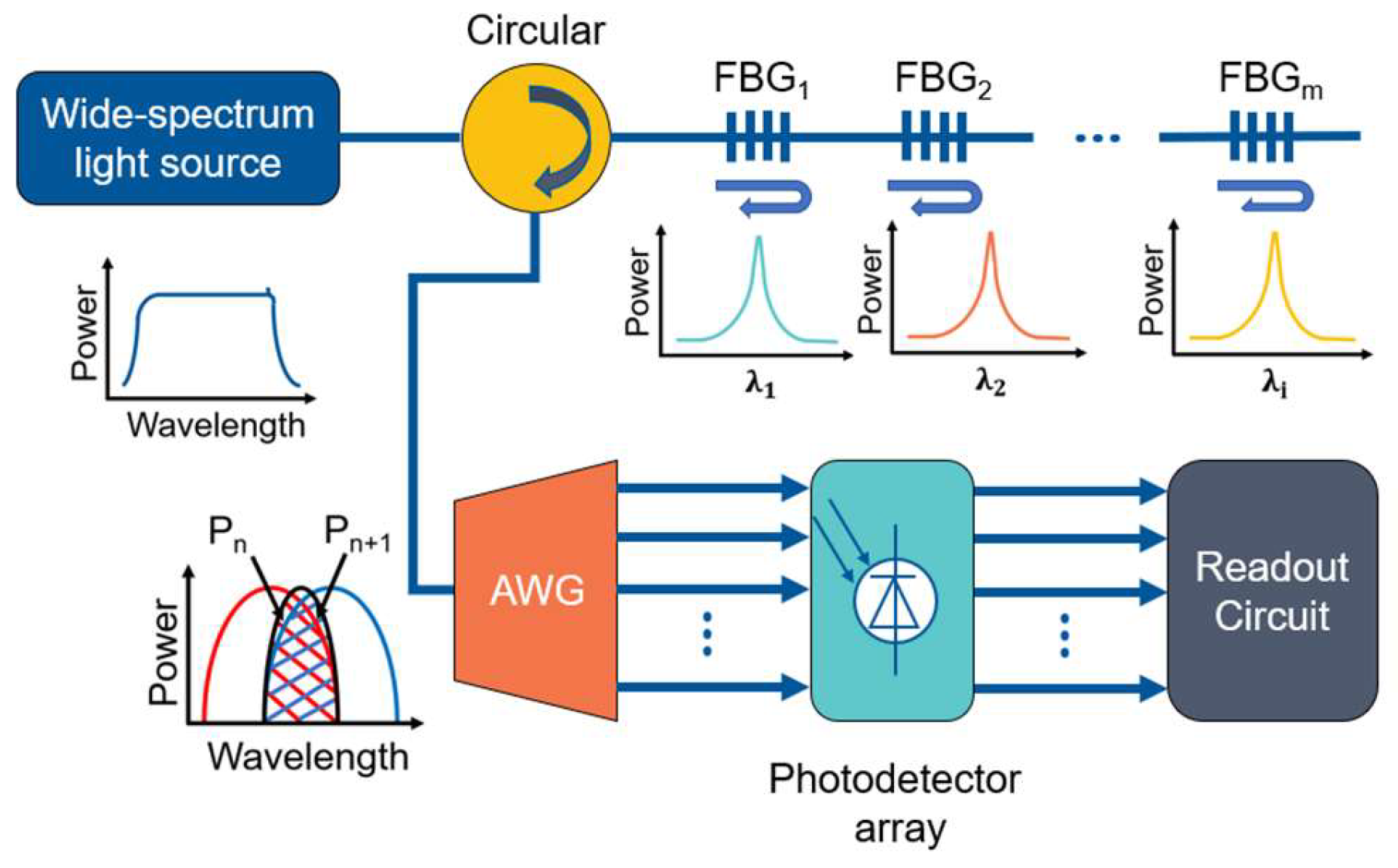
:1. Introduction
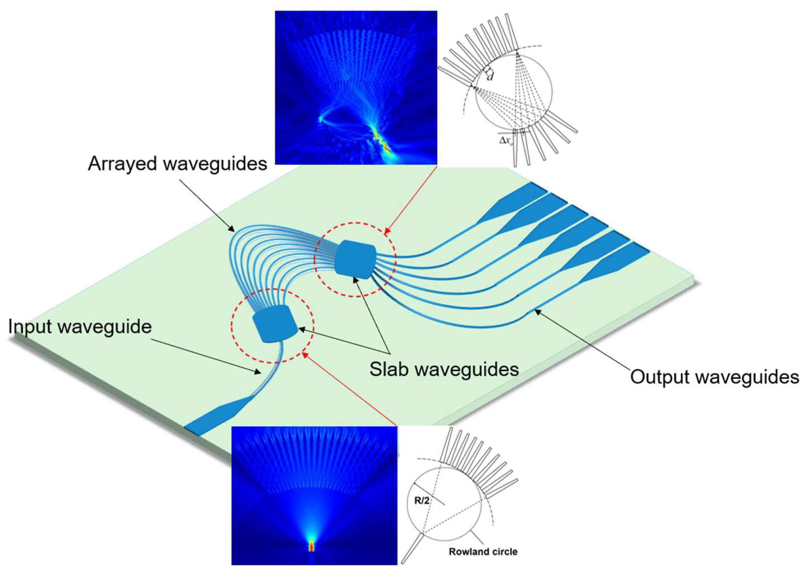
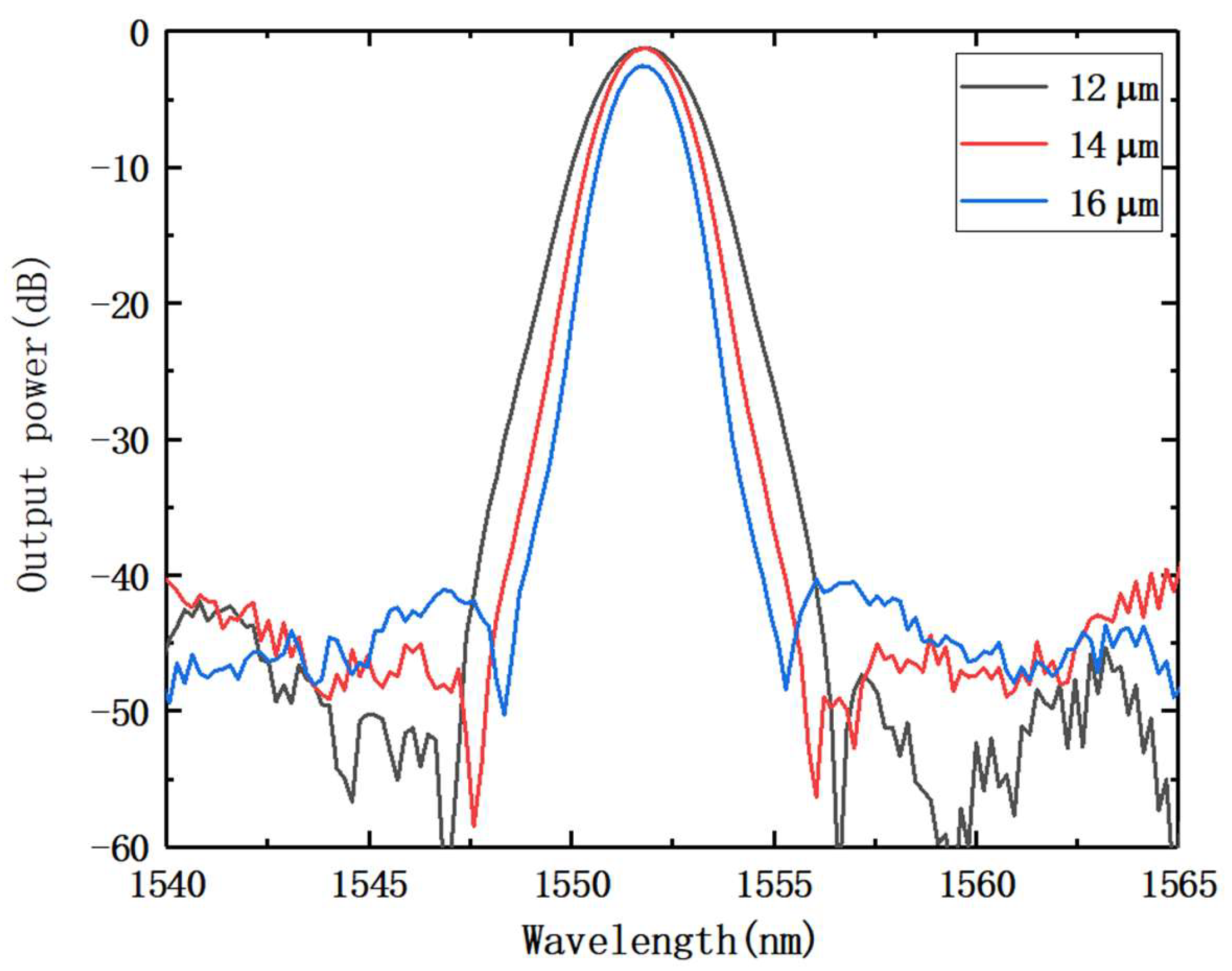
2. Design and Simulation
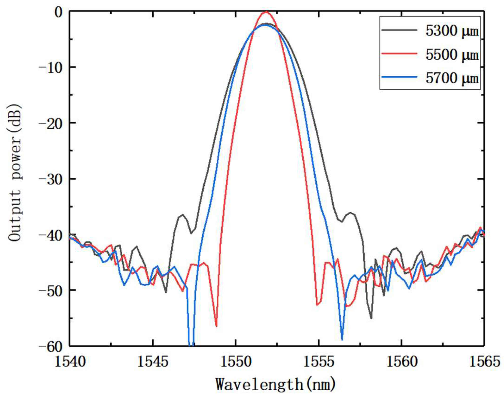
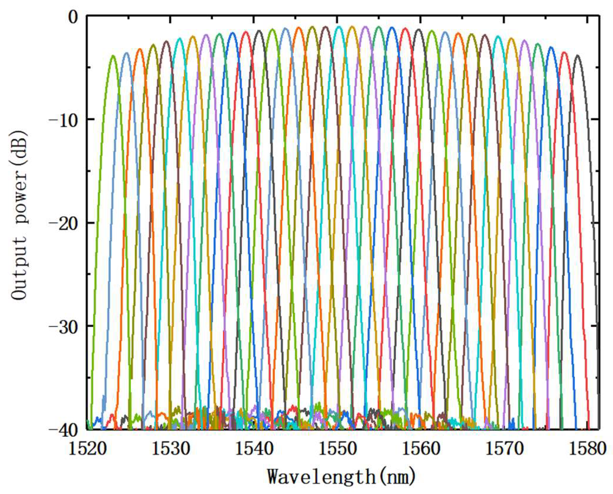
3. Experimental Measurement
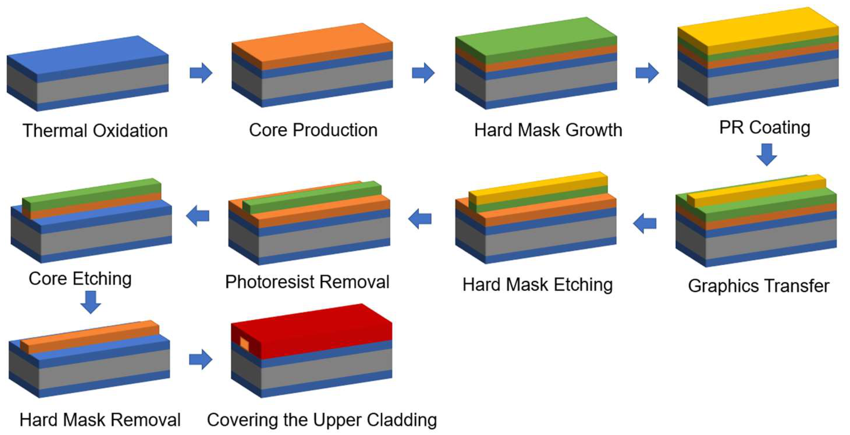
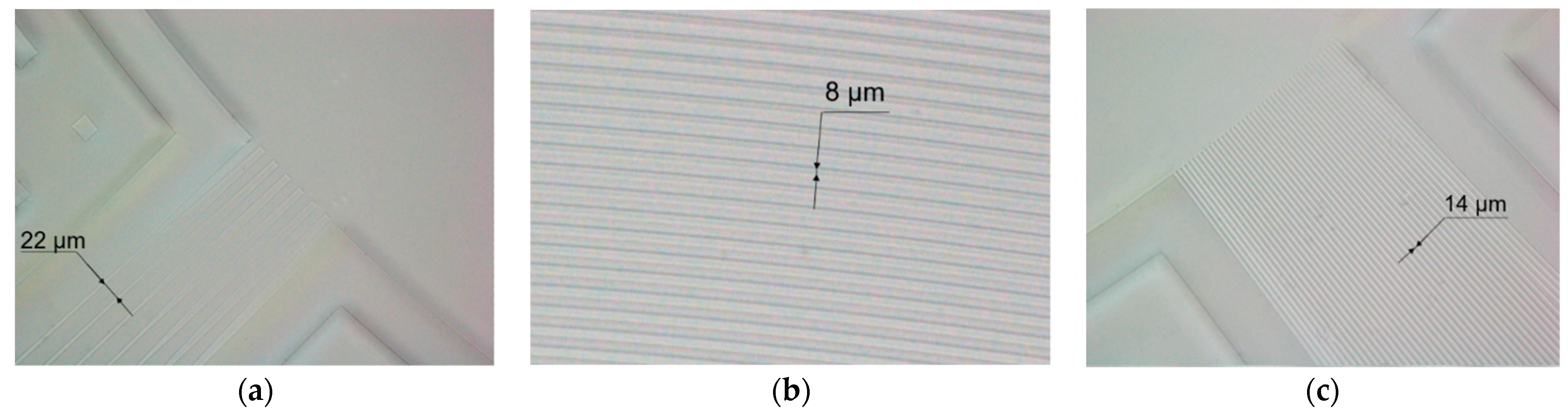
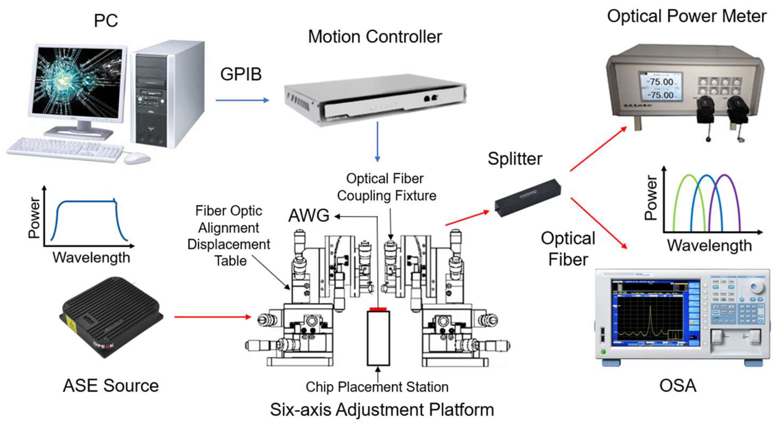
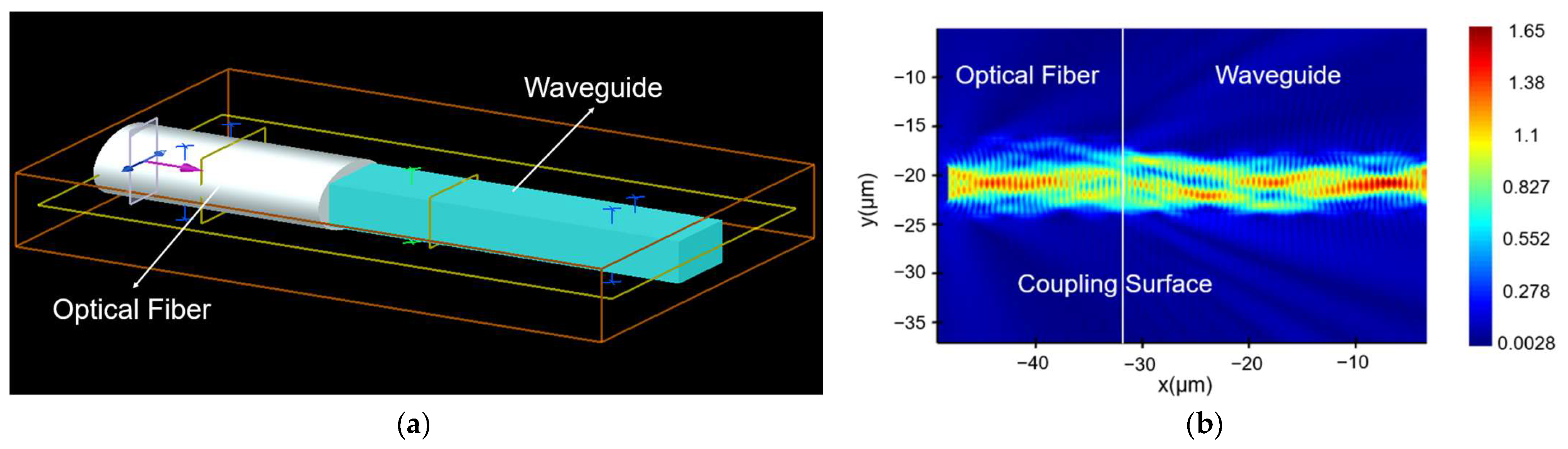
3.1. Fabrication
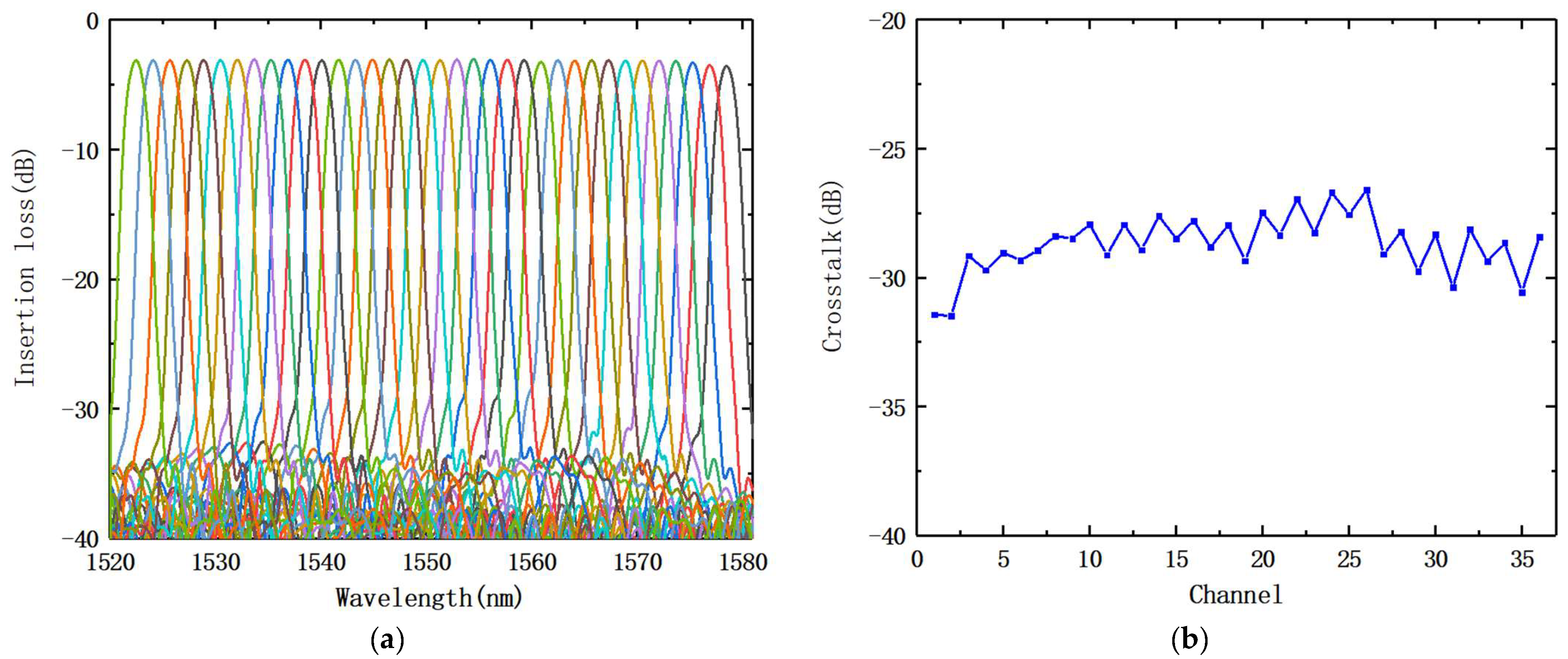
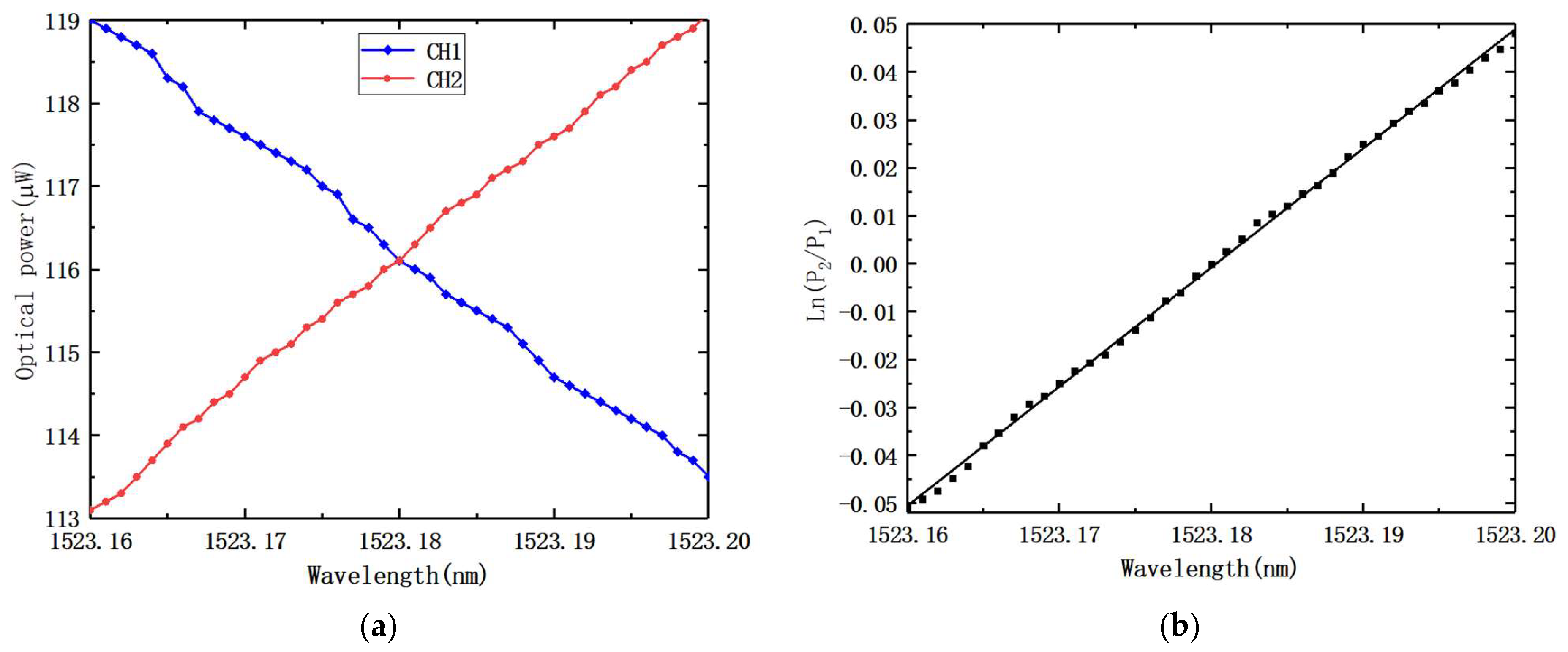
3.2. Measurement
4. Conclusions
Author Contributions
Funding
Institutional Review Board Statement
Informed Consent Statement
Data Availability Statement
Acknowledgments
Conflicts of Interest
References
- Xu, G.; He, B.; Li, H.; Gui, X.; Li, Z. FBG pressure sensor in pressure distribution monitoring of ship. Opt. Express 2022, 30, 21396–21409. [Google Scholar] [CrossRef]
- Szebényi, G.; Blößl, Y.; Hegedüs, G.; Tábi, T.; Czigany, T.; Schledjewski, R. Fatigue monitoring of flax fibre reinforced epoxy composites using integrated fibre-optical FBG sensors. Compos. Sci. Technol. 2020, 199, 108317. [Google Scholar] [CrossRef]
- Kuhn, G.G.; Sousa, K.M.; Martelli, C.; Bavastri, C.A.; da Silva, J.C.C. Embedded FBG Sensors in Carbon Fiber for Vibration and Temperature Measurement in Power Transformer Iron Core. IEEE Sensors J. 2020, 20, 13403–13410. [Google Scholar] [CrossRef]
- Karatas, C.; Degerliyurt, B.; Yaman, Y.; Sahin, M. Fibre Bragg grating sensor applications for structural health monitoring. Aircr. Eng. Aerosp. Technol. 2019, 92, 355–367. [Google Scholar] [CrossRef]
- Hsu, C.-Y.; Chiang, C.-C.; Hsieh, T.-S.; Chen, T.-H.; Chen, Y.-H. A study of strain measurement in cylindrical shells subjected to underwater shock loading using FBG sensors. Optik 2020, 217, 164701. [Google Scholar] [CrossRef]
- Tsai, J.-P.; Ho, Y.-T.; Wang, Y.-L.; Chang, L.-C.; Wang, T.-B. An Optical System for Monitoring Groundwater Pressure and Temperature Using Fiber Bragg Grating. Opt. Express 2021, 29, 16032–16045. [Google Scholar]
- Guo, K.; He, J.; Shao, L.; Xu, G.; Wang, Y. Simultaneous Measurement of Strain and Temperature by a Sawtooth Stressor-Assisted Highly Birefringent Fiber Bragg Grating. J. Light. Technol. 2020, 38, 2060–2066. [Google Scholar] [CrossRef]
- Gassino, R.; Perrone, G.; Vallan, A. Temperature Monitoring with Fiber Bragg Grating Sensors in Nonuniform Conditions. IEEE Trans. Instrum. Meas. 2019, 69, 1336–1343. [Google Scholar] [CrossRef]
- Kojima, S.; Hongo, A.; Komatsuzaki, S.; Takeda, N. High-speed optical wavelength interrogator using a PLC-type optical filter for fiber Bragg grating sensors. In Proceedings of the Smart Structures and Materials 2004: Smart Sensor Technology and Measurement Systems, San Diego, CA, USA, 14 March 2004; pp. 241–249. [Google Scholar]
- Wang, J.; Xu, S.; Chen, J.; Zou, W. A Heterogeneous Silicon on Lithium Niobate Modulator for Ultra-Compact and High-Performance Photonic Integrated Circuits. IEEE Photon- J. 2021, 13, 1–12. [Google Scholar] [CrossRef]
- Zhang, W.; Yao, J. Photonic integrated field-programmable disk array signal processor. Nat. Commun. 2020, 11, 406. [Google Scholar] [CrossRef] [PubMed]
- Theurer, M.; Moehrle, M.; Sigmund, A.; Velthaus, K.-O.; Oldenbeuving, R.M.; Wevers, L.; Postma, F.M.; Mateman, R.; Schreuder, F.; Geskus, D.; et al. Flip-Chip Integration of InP to SiN Photonic Integrated Circuits. J. Light. Technol. 2020, 38, 2630–2636. [Google Scholar] [CrossRef]
- Mukherjee, A.K.; Xiang, M.; Preu, S. Broadband Terahertz Photonic Integrated Circuit with Integrated Active Photonic Devices. InPhotonics 2021, 8, 492. [Google Scholar] [CrossRef]
- Liu, Y.; Wang, Z.; Liu, Y.; Wang, X.; Guo, X.; Li, D.; Yao, Y.; Song, Q.; Du, J.; He, Z.; et al. Ultra-Compact Mode-Division Multiplexed Photonic Integrated Circuit for Dual Polarizations. J. Light. Technol. 2021, 39, 5925–5932. [Google Scholar] [CrossRef]
- Mendoza, E. Fully integrated miniature multi-point fiber Bragg grating sensor interrogator (FBG-transceiver™) system for applications where size weight and power are critical for operation. In Proceedings of the European Workshop on Structural Health Monitoring, Dresden, Germany, 3–6 July 2012; pp. 1–7. [Google Scholar]
- Li, H.; An, Z.; Zhang, S.; Zuo, S.; Zhu, W.; Zhang, S.; Huang, B.; Cao, L.; Zhang, C.; Zhang, Z. Fully Photonic Integrated Wearable Optical Interrogator. ACS Photonics 2021, 8, 3607–3618. [Google Scholar] [CrossRef]
- Ke, L.; Ming, D.; Pei, Y.; Li, L.; Guang, S.; Lian, Z. Review of fiber Bragg grating interrogation techniques based on array waveguide gratings br. Acta Physica Sinica 2022, 71, 094207. [Google Scholar]
- Marin, Y.E.; Nannipieri, T.; Oton, C.J.; Di Pasquale, F. Current Status and Future Trends of Photonic-Integrated FBG Interrogators. J. Light. Technol. 2018, 36, 946–953. [Google Scholar] [CrossRef]
- Evenblij, R.; Leijtens, J. Space Gator: A giant leap for fiber optic sensing. In Proceedings of the International Conference on Space Optics—ICSO 2014, Tenerife, Spain, 6–10 October 2014; pp. 373–380. [Google Scholar]
- Li, H.; Xie, R.; Hong, Y.; Zhang, Z.; Zhang, C.; Tang, C.; Li, E.J. Effect of polarization sensitivity on ultrasmall silicon-on-insulator-based arrayed waveguide grating for fiber Bragg grating sensor interrogation. Opt. Eng. 2018, 57, 065103. [Google Scholar] [CrossRef]
- Yuan, P.; Weng, S.; Ji, S.; Zhang, D.; Zhu, L. Performance analysis of fiber Bragg grating sensor interrogators based on arrayed waveguide gratings. Opt. Eng. 2021, 60, 066101. [Google Scholar] [CrossRef]
- Ji, S.; Li, K.; Yuan, P.; Sun, G.; Lu, L.; Meng, F.; Lu, Y.; Zhu, L. Design and fabrication of AWG with large bandwidth applied in FBG interrogation system. Opt. Laser Technol. 2022, 149, 107372. [Google Scholar] [CrossRef]


| Parameters | Value |
|---|---|
| Central wavelength | 1551 nm |
| Number of input/output ports | 7 in/36 out |
| Adjacent arrayed waveguide spacing | 8 µm |
| Channel spacing | 1.6 nm |
| Adjacent input waveguide distance | 22 µm |
| Adjacent output waveguide distance | 14 µm |
| Rowland circle diameter | 5626.669 µm |
| Adjacent waveguide spacing | 19.24235 µm |
| Parameters | Value |
|---|---|
| 3-dB bandwidth | 1.76 nm |
| Insertion loss (IL) | 3.46 dB |
| Crosstalk | −29.76 dB |
| Channel | Center Wavelength |
|---|---|
| CH1 | 1522.4 nm |
| CH2 | 1524.0 nm |
| CH3 | 1525.6 nm |
| CH36 | 1578.4 nm |
Publisher’s Note: MDPI stays neutral with regard to jurisdictional claims in published maps and institutional affiliations. |
© 2022 by the authors. Licensee MDPI, Basel, Switzerland. This article is an open access article distributed under the terms and conditions of the Creative Commons Attribution (CC BY) license (https://creativecommons.org/licenses/by/4.0/).
Share and Cite
Li, K.; Yuan, P.; Lu, L.; Dong, M.; Zhu, L. PLC-Based Arrayed Waveguide Grating Design for Fiber Bragg Grating Interrogation System. Nanomaterials 2022, 12, 2938. https://doi.org/10.3390/nano12172938
Li K, Yuan P, Lu L, Dong M, Zhu L. PLC-Based Arrayed Waveguide Grating Design for Fiber Bragg Grating Interrogation System. Nanomaterials. 2022; 12(17):2938. https://doi.org/10.3390/nano12172938
Chicago/Turabian StyleLi, Ke, Pei Yuan, Lidan Lu, Mingli Dong, and Lianqing Zhu. 2022. "PLC-Based Arrayed Waveguide Grating Design for Fiber Bragg Grating Interrogation System" Nanomaterials 12, no. 17: 2938. https://doi.org/10.3390/nano12172938
APA StyleLi, K., Yuan, P., Lu, L., Dong, M., & Zhu, L. (2022). PLC-Based Arrayed Waveguide Grating Design for Fiber Bragg Grating Interrogation System. Nanomaterials, 12(17), 2938. https://doi.org/10.3390/nano12172938