Article

Gain Enhancement of the Optical Waveguide Amplifier Based on NaYF4/NaLuF4: Yb, Er NPs-PMMA Integrated with a Si3N4 Slot

Department of Communication Engineering, Jilin University, Changchun 130012, China
*
Author to whom correspondence should be addressed.
Nanomaterials 2022, 12(17), 2937; https://doi.org/10.3390/nano12172937
Submission received: 20 July 2022 / Revised: 20 August 2022 / Accepted: 22 August 2022 / Published: 25 August 2022

Abstract

:
A Si3N4 slot waveguide has the ability to confine light tightly in the slot, shows weak absorption of 980 nm pump light, and has lower transmission loss compared to a Si slot. Hence, the optical waveguide amplifier based on Er3+ and Yb3+codoped was proposed to be integrated with a Si3N4 slot to increase the gain. The core-shell NaYF4/NaLuF4: 20%Yb3+, 2%Er3+ nanocrystals-polymeric methyl methacrylate covalent linking nanocomposites were synthesized and filled into the slot as gain medium. The concentrations of Er3+ and Yb3+ were increased compared with traditional physical doping methods. High-efficiency emission at 1.53 μm was achieved under 980 nm laser excitation. The slot waveguide was accurately designed using the semivector finite difference method in combination with the maximum confinement factors and the minimum effective mode area. The optimum width of the slot was 200 nm, and the optimum height and width of the silicon strip waveguide were 400 nm and 400 nm, respectively. The six-level spectroscopic model was presented, and the gain characteristics of the slot waveguide amplifier were numerically simulated. A net gain of 8.2 dB was achieved, which provided new ideas and directions for waveguide amplifiers.

1. Introduction

Research of integrated optics has developed rapidly [1,2,3]. The diverse passive and active nanophotonic devices based on silicon-on-insulator (SOI) waveguides and silicon nitride (Si3N4) waveguides such as modulators [4,5], filters [6,7], wavelength division multiplexers [8,9], and detectors [10,11] have been widely developed and have shown numerous applications in many fields. However, challenges still exist. Loss of the large-scale on-chip integrated devices limits the device performance and increases the bit error rate of the signal, which hinders the development of large-scale integration [12,13]. On-chip erbium-doped waveguide optical amplifier (EDWA) can compensate for the loss effectively [14,15,16,17]. It is an efficient way to overcome this problem. Si and Si3N4 cannot efficiently perform the task of integrating optical interconnections alone. Therefore, it is highly necessary to integrate with other active materials. The novel slot waveguide, which can strongly confine the light in a narrow slot region of low refractive index material [18,19,20], is more likely to integrate with other materials than the traditional strip waveguide. The density of the light field in the slot is nearly 20 times higher than that of a conventional rectangular dielectric waveguide and will promote the signal and pump interaction with the gain medium. This kind of waveguide amplifier based on slots is of great value for improving the gain performance and reducing the threshold pump power. In recent years, few reports regarding the optical waveguide amplifiers based on slots integrated with erbium-doped materials have been reported. In 2012, the Er/Yb silicate slot waveguide amplifier was fabricated and achieved a signal 1.7 dB gain at 1.53 μm in a waveguide with a 6 mm long slot pumped at 1476 nm when the Er3+ concentration was confirmed to be 1 × 1027  m−3 [21]. However, the inorganic material is difficult to integrate with slots because of the complicated technology, expensive equipment, and long cycle. Erbium-doped polymer materials have the outstanding advantages of high bandwidth, low cost, species diversity, and ease of realizing large-scale and high-density integration [22,23,24,25]. Integrating with slots for EDWA fabrication is a good decision. In 2014, the potential for large optical gain improvement of erbium-doped rich polymers integrated into silicon-slot waveguides amplifier pumped at 1480 nm was shown [26]. In 2020, the gain characteristics of the hybrid slot waveguide amplifiers integrated with NaYF4:Er3+ NPs-PMMA pumped at 1480 nm were analyzed. A net gain of 5.78 dB was achieved with the length of 1.5 cm when the Er3+ concentration was 1.3 × 1027 m−3 [27]. In this case, the gain of the slot waveguide amplifier with the polymer as gain medium is still not ideal. This is mainly because Si has strong absorption of 980 nm light. Therefore, 1480 nm was chosen as a pump and pure erbium-doped polymer as gain medium. The low-pumping efficiency at 1480 nm and the low-Er3+-luminescence intensity of pure erbium-doped materials without Yb3+ sensitization limited the amplification properties which could not meet the requirements of optical communications. To overcome this issue, a Si3N4 platform with low loss and a weak absorption effect on 980 nm was employed [28,29]. A Si3N4 slot instead of slot-based Si confined the light field in the slot region tightly. Er3+ and Yb3+codoped polymer material was used as gain medium.
In this work, the core-shell α-NaYF4/β-NaLuF4: Yb3+, Er3+ nanocrystals were synthesized using a mild hydrothermal method and then copolymerized with methyl methacrylate (MMA) to fabricate NaYF4/NaLuF4: Yb, Er NPs-PMMA as gain medium. The fluorescence emission intensity of the nanocrystals coated with the shell increased nearly six times compared to α-NaLuF4. The doped Er3+ concentrations had been increased an order compared with traditional physical doping methods. The Er3+ concentration doped was 2.8 × 1026 m−3. The slot waveguide was optimized by the semivector finite difference method considering the maximum confinement factors and the minimum effective mode area. The optimum width of the slot was 200 nm, and the optimal height and width of the silicon strip waveguide were 400 nm and 400 nm, respectively. The six-level spectroscopic model was presented, and the gain characteristics of the slot waveguide amplifier were numerically simulated. A net gain of 8.2 dB was when the transmission loss was 3 dB/cm. The gain was enhanced compared with the silicon slot waveguide amplifier even though the pure Er3+ concentration doped was nearly ten times higher than the Er3+ and Yb3+ codoped polymer material. It provided new ideas and directions for waveguide amplifiers.

2. Experiments Details

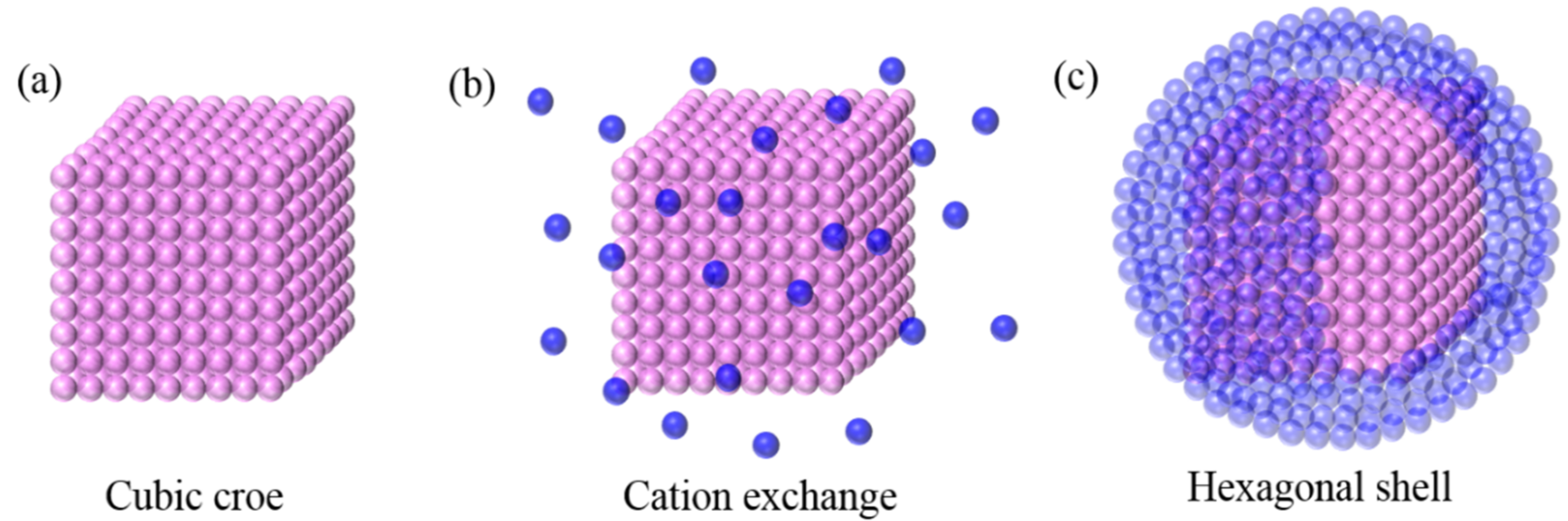
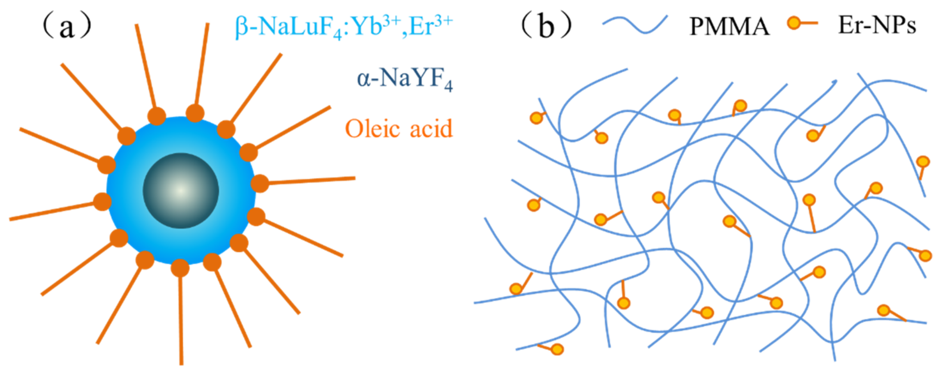
2.1. Preparation of NaYF4/NaLuF4: Yb, Er NPs-PMMA

The performance of medium gain material is an important factor affecting EDWA gain, particularly the Yb-Er ion doping concentration and the luminescence intensity. However, these two factors are often incompatible. On the one hand, small-sized nanoparticles tend to disperse easily in polymer matrix materials, but they have a large specific surface area and a significant surface luminescence quenching phenomenon, which in turn affects the luminescence intensity of nanoparticles. Larger-sized nanoparticles cause light scattering in the device, which leads to additional losses. On the other hand, nanoparticles are usually incorporated into polymer materials in a physically doped manner. Er3+ exists as inorganic salts and is poorly compatible with organic polymers, resulting in a low concentration of Er3+ optical activity in polymer matrix materials, in addition, the stability of the material also needs to be improved. Therefore, we carried out shell coating on the surface of rare-earth doped nanoparticles to improve the luminescence intensity of the nanoparticles and used the modification of unsaturated groups on the surface of nanoparticles to bond nanoparticles to polymer monomers through chemical bonds, which can greatly improve the incorporation of nanoparticles into polymers while solving the problems of easy agglomeration, low solubility, and poor stability of nanoparticles in polymers.
The core-shell nanoparticles were synthesized using a mild hydrothermal method. In this condition, the unsaturated perssad on the surface of nanoparticles was protected by reacting at a relatively low temperature. The heterogeneous induction procedure was explored, as shown in Figure 1. The process is mainly divided into two major steps: first, was the preparation of the pure cubic phase of nuclear nanomaterial α-NaYF4. A total of 0.6 g of NaOH powder was dissolved in a solution of 20 mL oleic acid, 10 mL ethanol, and 10 mL deionized water and mixed by stirring to dissolve fully as a clear solution. A total of 0.5 mmol of YCl3·6H2O powder was weighed and dissolved in 4 mL of deionized water and stirred thoroughly to form a solution, and this solution was added dropwise to the above solution and stirred continuously until it was a homogeneous dissolution. A total of 2 mmol of KF·2H2O solid was dissolved in 4 mL of deionized water. It was stirred continuously until the solution was slowly dripped into the above-mixed solution and then stirred well to obtain a semi-white solution. This well-mixed solution was divided equally into two polytetrafluoroethylene-lined high-pressure reactors, heated at 160 °C for 240 min, and cooled to room temperature to obtain a mixed solution containing α-NaYF4 nanoparticles. Then, the shell growth link was performed. A total of 0.3 g NaOH powder was weighed and dissolved in 10 mL oleic acid, 5 mL ethanol, and 1 mL deionized water to prepare a solution. A 20 mL solution containing α-NaYF4 nuclear nanoparticles was mixed with the above solution and stirred. A total of 0.195 mmol of LuCl3·6H2O powder, 0.05 mmol of YbCl3·6H2O powder, and 0.005 mmol of ErCl3·6H2O solid were weighted and dissolved in 2 mL of deionized water. A mixture of nuclear nanoparticles was slowly dropped and stirred continuously to form a homogeneous solution. A total of 2 mmol of KF·2H2O was dissolved in 2 mL of deionized water and stirred vigorously and continuously to obtain the mixture. Then it was dispensed into two polytetrafluoroethylene-lined high-pressure reactors and heated at 160 °C for 480 min for the second-step crystal-growth process, during which cation exchange occurred between the newly added Lu3+ and Y3+. A NaYxLu(1-x)F4 heterointerface was formed on the nuclear surface. Lattice mismatches of NaYF4 and NaLuF4 could provide additional driving forces to trigger the cubic-to-hexagonal phase transition. At the end of growth, the mixture was slowly dropped to room temperature, centrifuged, and vacuum-dried to obtain a white powder, core-shell structure NaYF4/NaLuF4: 20%Yb3+, and 2%Er3+ nanoparticles.

2.2. Characterization of NaYF4/NaLuF4: Yb, Er NPs-PMMA

A spot of the nanoparticles powder was dissolved in cyclohexane to form a transparent solution and dropped onto a carbon film copper mesh. The morphology and size of the nanoparticles were observed with Hitachi H-600 transmission electron microscopy. The TEM images of the nuclear α-NaYF4 material are presented in Figure 2a. The nanoparticles with a regular square shape were dispersed uniformly. The particle size we measured was within the range of 10–15 nm, as shown in Figure 2c. The average particle size of nuclear NaYF4 nanoparticles was around 13 nm, according to Scheller’s formula. TEM images of the nanoparticles coated shell are shown in Figure 2b. The morphology of the nanoparticles appeared spherical, which was because the size of the hexagon tended to be spherical when it was small. They were dispersed uniformly without agglomeration. Compared with uncoated particles, the size of the particle was increased; as shown in Figure 2d, the size of the nanoparticles after shell coating was approximately 21 nm.
The nanoparticles we synthesized were coated with oleic acid. The C=C, C=O double bonds from oleic acid ligands were protected well using the solvothermal method. Nanoparticles were chemically bonded to the polymer monomer using unsaturated ligand double bonds, and a schematic image of the covalent linking nanocomposites is shown in Figure 3. We dissolved 0.1 mmol nanoparticles in 4 mL butyl acetate. A total of 10 g methyl methacrylate (MMA) was weighed and dissolved in 2 mL butyl acetate. Then, polymerization initiator azobisisobutyronitrile (ABIN) was added together in a single-port flask. We put the flask in an oil bath followed by heating (65 °C) and stirring for 60 min to complete the prepolymerization reaction. The solution containing nanoparticles was added dropwise into the flask. We increased the temperature of the oil bath (80 °C) and continuously stirred it to achieve the copolymerization reaction. The NPs-PMMA covalent linking nanocomposites were obtained by free-radical polymerization, ionic polymerization, and the polymerization of nanoparticles with organic polymer monomers under the catalyzation of free-radical initiators and ionic-type initiators. The doped Er3+ concentration was enhanced to 2.8 × 1026 m−3, which was increased compared to traditional physical doping.
The critical properties of film forming, emission spectra, and absorption spectra of the gain medium were characterized and were found to impact the gain performances of EDWA. The NPs-PMMA was spin-coated on Si and heated by 120 °C for 2 h in the oven to form a 7 μm-thick film. Atomic force microscopy (AFM) was used to characterize the film-forming properties of the material shown in Figure 4a,b. As shown, the film surface was flat and smooth without nanoparticle precipitation. The surface roughness of the film was measured to be only 0.349 nm (scan area 20 μm × 20 μm), which was an order of magnitude lower than traditional physical doping. This suggests that it is an ideal material for preparing waveguide devices. The infrared emission spectrums pumped by 980 nm of the α-NaYF4/β-NaLuF4: Er3+, Yb3+ NPs, and α-NaLuF4 NPs with the same doping concentration were measured. As illustrated in Figure 4c, the main emission peak of both materials was at 1530 nm, corresponding to the 4I13/2→4I15/2 energy level transition of Er3+. Nanoparticles coated with a shell had a stronger emission than cubic-phase NaLuF4 of the same size. The fluorescence performance was significantly improved by nearly six times. The full width at half-maximum (FWHM) of the NaYF4/NaLuF4: Er, Yb NPs fluorescence spectrum was broadened to 62 nm. The absorption spectra of the core film were characterized by a Cary500 Scan UV-Vis-NIR spectrophotometer, as shown in Figure 4d. The typical transitions of ground-state Er3+ to each excited-state energy level corresponded to the absorption peaks in the figure. Yb3+ was codoped in, and the absorption peak at 976 nm was much stronger than that of pure doped Er3+, which facilitated the absorption and improved the efficiency rate of pump light.

2.3. Optimization of the Slot Waveguide

The electric field intensity in the vertical medium interface at the sidewall will be modified by the factor of n S i 3 N 4 2 n N C s P M M A 2 because of the electric displacement continuity boundary condition (D = εE) for the horizontal dielectric. Then, the light can be confined within the nanoscale low-refractive index slot, contributing to the high light intensity. A schematic image of the slot waveguide is shown in Figure 5a. Taking advantage of the high electric field intensity, the interaction between the signal light, pump light, and gain medium will be promoted. The stronger the ability of the slot waveguide to limit the light field, the stronger the interaction with the gain medium, and greater gain can be achieved. Meanwhile, a smaller effective cross-sectional area of the slot waveguide can facilitate a reduction in the threshold power of EDWA. Therefore, we optimized the size of the slot waveguide in terms of both the ability to confine the light and the effective cross-sectional area. We filled the NaYF4/β-NaLuF4: Er, Yb NCs-PMMA into the slot as gain medium and measured its refractive index with an ellipsometer, as shown in Figure 5b. The measured values of the core layer were 1.512 at 1530 nm and 1.52 at 980 nm, respectively.
The finite element method (FEM) was used to analyze the modal profiles of the Si3N4 slot waveguide with a height (Hr) of 450 nm, width (Wr) of 450 nm, and slot width (Ws) of 200 nm. The optical field distributions under TE and TM polarization at 1530 nm are shown in Figure 6a,b, respectively. The optical field distributions under TE and TM polarization at 980 nm are shown in Figure 6c,d respectively.
Under TE polarization, the slot can confine the light well, while more light fields leak into the upper and lower cladding under TM polarization. This was not conducive to the interaction between the light field and the gain polymer. Therefore, we only considered the TE polarization mode, and the related parameters under the TM polarization mode in this paper were only used for reference and comparison.

2.3.1. Optimization of Slot Waveguides Combined with Maximum Confinement Factors

For a more intuitive view of the slot’s ability to restrict the light, we defined the overlapping integration factor ΓS of the slot waveguide to represent the effective utilization of energy, as shown in Equation (1), so we searched for a maximum in all the considered cases, which could be used to achieve higher gain [30]. The finite difference method (FDM) was used to calculate ΓS to primarily optimize the height of Si3N4 (Hr), the width of Si3N4 (Wr), and the slit width (WS).
Γ S = S E ( x , y ) 2 d x d y T o t a l E ( x , y ) 2 d x d y
First, the effective refractive index (Neff) and ΓS were calculated as a function of the width of Wr at 1530 nm and 980 nm under TE and TM polarizations shown in Figure 7a,b. The wavelength interval between the 980 nm pump light and signal light was quite large; the optical field distribution was significantly different. Then, the Neff and ΓS of the waveguide at signal wavelengths were quite different from those of pump wavelengths. Under the TE polarization mode, the light field was confined in the slot well. With increasing Wr, Neff also increased, and ΓS at 980 nm gradually decreased. At the same time, ΓS at 1530 nm tended to saturate when Wr increased to 400 nm. This is due to the low impact of Wr at 1530 nm on the waveguide light field. At 980 nm, the light field was mostly confined to the Si3N4 strip waveguide. As Wr increased, more light fields were confined to the Si3N4 strip waveguide. As a result, Neff increased while ΓS gradually decreased. Next, we optimized WS combined with the Neff and ΓS curves at the signal and pump wavelengths under TE and TM polarizations, as revealed in Figure 7c,d. The curves under TE polarization tend to be basically consistent with that of TM polarization. When WS increased, Neff decreased. Additionally, ΓS at a 980 nm wavelength decreased rapidly, increasing WS. It increased to extreme values and then decreased rapidly. ΓS increased rapidly at 1530 nm as WS increased and tended to be saturated. Maximum ΓS was obtained when WS was 200 nm. This is because with increased WS, light field leakage to the upper and lower cladding was gradually controlled, and more light fields were included in the slot. Therefore, ΓS increases rapidly at this time, accompanied by a rapid decrease in Neff. However, with increased WS, the coupling resonance of the abrupt light field at the interface between slot dielectrics was weakened. Thus, the confinement of the light field in the slot was impaired, and some light fields leaked to the cladding. As a result, Neff and ΓS gradually decreased, and the rate of decrease in Neff became slower. Combined with the dependence of Neff and ΓS on the different widths of Hr shown in Figure 7e,f, we optimized the Hr of the waveguide. Hr is the main factor affecting ΓS. For any waveguide slot size, increasing its Hr will make ΓS increase. As Hr increased, both Neff and ΓS increased monotonically. Since the light at 980 nm already confined most of the light to the Si3N4 strip waveguide, it continued to increase its height and had little effect on ΓS. Meanwhile, too high an Hr led to an increase in transmission loss and introduced extra difficulty to the coupling between the optical fiber and the end face of the waveguide.

2.3.2. Optimization of Slot Waveguide Combined with Minimum Effective Mode Area
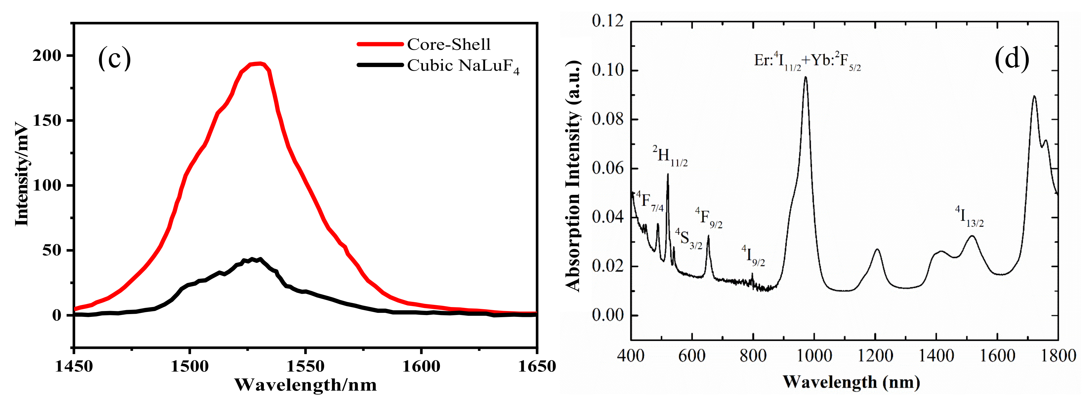
We combined the effective cross-sectional area (Aeff) to further optimize the size of the slot. The definition formula for Aeff is shown in Equation (2) [27]:
A e f f = ( E ( x , y ) 2 d x d y ) 2 E ( x , y ) 4 d x d y
The higher the ΓS value, the higher the obtained gain. The smaller the Aeff, the smaller the threshold pump power. As shown in Figure 8, we calculated Aeff for different slot sizes. The Aeff under TE polarization at the same wavelength was much smaller than the Aeff under TM polarization. Thus, only the TE polarization mode was analyzed in this paper. As shown in Figure 8a, with increasing Wr, Aeff first decreased quickly at the wavelength 1530 nm. When Wr reached 400 nm, Aeff tended to saturate. Aeff remained almost unchanged as Wr increased at 980 nm. Combined with the joint analysis of Figure 7a,b, 400 nm was demonstrated to be the optimal value for Wr. Different WS and Aeff relationship curves under TE and TM polarizations at 1530 nm and 980 nm are shown in Figure 8b for when Hr was 400 nm and Wr was 400 nm. Aeff slowly increased. As WS increased from 50 nm to 500 nm at 980 nm, Aeff increased by less than 0.1 μm2. Thus, Aeff at 1530 nm was mainly considered along with the increase in WS. Aeff curves trended along linear growth. Combined with the joint analysis of Figure 7c,d, 200 nm was demonstrated to be the optimal value for WS. Aeff with different Hr under TE and TM polarization at 1530 nm and 980 nm wavelengths were simulated in Figure 8c for when Wr was 400 nm and WS was 200 nm. Aeff slowly increased with an increase in Hr at the pump wavelength. Aeff first decreased rapidly to an extreme value and then slowly increased with the increase in Hr at a signal wavelength. Combined with the joint analysis of Figure 7e,f, we believe that 400 nm is the best-optimized value for Hr. In this condition, under TE polarization, ΓS is 0.1500 and 0.1753, and Aeff is 1.3829 µm2 and 0.6436 µm2 in the slit region at 1530 nm and 980 nm wavelengths, respectively.

3. Results

The novel Er and Yb codoped waveguide amplifiers were presented by integrating NaYF4/NaLuF4: Er3+, Yb3+ NCs-PMMA with a Si3N4 slot waveguide. To analyze the gain performance of the device accurately, we established a transition model of an Er-Yb codoped six-level system pumped at 980 nm, as shown in Figure 9a. The Yb3+ ions in the ground state 2F7/2 were excited by a 980 nm pump absorbing the energy and then transitioned upward to level 2F5/2. Because 2F5/2 and 2F7/2 levels of Yb3+ had the same energy spacing between Er3+ 4I11/2 and 4I15/2 levels, and erbium ytterbium atoms were very far apart, Yb3+ ions rapidly transmitted energy to Er3+ ions in the ground state by cross-relaxation. Thus, they transited from the 4I15/2 level to the excited-state level 4I11/2. Due to the instability of 4I15/2, Er3+ ions quickly transferred to the metastable state 4I13/2 through the nonradiative relaxation to form population inversion. Then, they transitioned down to the ground state 4I15/2 by excited emission and emitted photons with the same frequency as the signal light. The amplification of the signal light was realized. To build an accurate simulation model, we also considered cooperative up-conversion Cup between metastable levels 4I13/2 and 4I9/2, 4I15/2. Spontaneous radiation transitions from 4I9/2, 4I11/2, and 4I13/2 to their next levels were taken into account, as well as 2F5/2Yb to 2F7/2Yb. Amplified spontaneous emission (ASE) was neglected. A six-level spectroscopic model pumped at 980 nm was presented. The rate equations and propagation equations were solved. Incorporated with the characteristic parameters of the gain medium, the gain G at any point of the amplifier in the transmission direction z was calculated by the fourth-order Runge–Kutta method. G can be expressed in dB as:
G = 10 lg P S ( z ) P S ( 0 )
where PS(0) is the input signal power and PS(z) is the output signal power. As illustrated in Equation (3), a higher gain can be achieved with small input signal power. In combination with experimental experience, a 0.1 mW input power was selected. The Si3N4 slot waveguide amplifier was fabricated via the following steps: first, the Si3N4 film on SiO2 was first annealed at a high temperature of 1050–1150 °C for 3–7 h to remove the hydrogen bonds on the surface and inhibit the formation of O-H and N-H bonds before preparing the waveguide. The positive electron resistance ZEP520 with a thickness of 400 nm was spin-coated on the Si3N4 wafer. Then, the standard pattern exposure was performed using an electron beam. After image development and ICP (SPTS) etching for 140 s, the Si3N4 slot waveguide was obtained. Finally, a 3 µm-thick PMMA film was spin-coated onto the Si3N4 slot as the core layer and then baked at 120 °C for 2 h. The Si3N4 slot waveguide amplifier was obtained. We simulated the gain versus coordinate waveguide length with different transmission losses in Figure 9b. The optimal waveguide length corresponding to different transmission losses was different. The corresponding optimal waveguide length was longer when the transmission loss was smaller. When the transmission loss was only 2 dB/cm, the optimal waveguide length was approximately 8 cm, and a net gain of nearly 20 dB could be obtained. As transmission losses gradually increased, the gain values gradually decreased. No net gain was generated when the transmission loss was 5 dB/cm. This is mainly due to the small refractive index difference between Si3N4 and gain polymer materials, thus resulting in a smaller overlapping integration factor than the SOI slot waveguide. While the main advantage of preparing EYCDWA using a Si3N4 slot waveguide was the small transmission loss of the waveguide, a long waveguide could be used to improve the gain. At present, the minimum loss of the Si3N4 slot waveguide measured was approximately 3 dB/cm, the optimized length of the device was 6 cm, and the net gain obtained was approximately 8.2 dB. The doped Er3+ concentration will be further improved, and the optimum length of the waveguide will be shortened. Under the optimized conditions above, we simulated the gain characteristics of Si3N4 slot waveguide amplifiers with different slot widths, as shown in Figure 9c. The figure shows that the smaller the slot width, the smaller the pump threshold power is, which was associated with the Aeff of the waveguide. When the pump power was less than 300 mW, the gain increased with WS. Additionally, the gain values corresponding to each slot width were nearly overlapped as the pump power continued to increase. Therefore, the optimized range of WS was relatively larger. In this paper, considering polymer packing and transmission loss, the WS with 200 nm was selected as the optimized width. Figure 9d shows the gain versus pump power for different Wrs. Within this width range, the gain curves of each device almost completely coincided, mainly due to Wr not having direct effects on the light field. Within the Wr range of 300 nm to 450 nm, the gain presented minor variations. This feature provides convenient conditions for preparing devices and allows certain process tolerances.

4. Conclusions

In summary, we synthesized α-NaYF4/β-NaLuF4: Yb3+, Er3+ nanoparticles coated with oleic acid using a mild hydrothermal method, whose luminescence intensity was improved at 1.53 µm nearly six-fold. Then, the nanoparticles were copolymerized with methyl methacrylate (MMA) to fabricate NaYF4/NaLuF4: Yb, Er NPs-PMMA. The doped Er3+ concentration was 2.8 × 1026 m−3. NaYF4/NaLuF4: Yb, Er NPs-PMMA was filled into a Si3N4 slot waveguide as a core to promote the interaction between the light field and the Er-Yb codoped gain medium, and 980 nm was used as a pump light to improve the gain performance. The optimum size of the Si3N4 slot waveguide with an Hr of 400 nm, WS of 200 nm, and Wr of 400 nm were obtained by combining the confining factor and effective cross-sectional area via the finite difference method. A six-level system model of the Yb-Er codoped system was established, and the gain characteristics were simulated. Theoretically, when transmission loss was 3 dB/cm, a net gain of 8.2 dB could be obtained. With further optimization of loss and doped Er3+ concentration, ultrahigh gain can be envisaged.

Author Contributions

Conceptualization, G.H., X.L. and M.Z.; software, X.L.; formal analysis, X.L. and M.Z.; writing—original draft preparation, X.L. and M.Z.; writing—review and editing, G.H., X.L. and M.Z. All authors have read and agreed to the published version of the manuscript.

Funding

This work was supported by the National Natural Science Foundation of China (No. 61905088) and the Science and Technology Development Plan of Jilin Province (No. 20200401051GX).

Institutional Review Board Statement

Not applicable.

Informed Consent Statement

Not applicable.

Data Availability Statement

Not applicable.

Conflicts of Interest

The authors declare no conflict of interest.

References

  1. Ye, W.N.; Xiong, Y. Review of silicon photonics: History and recent advances. J. Mod. Opt. 2013, 60, 1299–1320. [Google Scholar] [CrossRef]
  2. Chen, X.; Li, C.; Tsang, H.K. Device engineering for silicon photonics. NPG Asia Mater. 2011, 3, 34–40. [Google Scholar] [CrossRef]
  3. Lim, A.E.-J.; Song, J.; Fang, Q.; Li, C.; Tu, X.; Duan, N.; Chen, K.K.; Tern, R.P.-C.; Liow, T.-Y. Review of Silicon Photonics Foundry Efforts. IEEE J. Sel. Top Quantum Electron. 2014, 20, 8300112. [Google Scholar] [CrossRef]
  4. Shiramin, L.A.; Van, D. Graphene Modulators and Switches Integrated on Silicon and Silicon Nitride Waveguide. IEEE J. Sel. Top. Quantum Electron. 2017, 23, 3600107. [Google Scholar]
  5. Lacava, C.; Cardea, I.; Demirtzioglou, I.; Khoja, A.E.; Ke, L.; Thomson, D.; Ruan, J.X.; Zhang, F.; Reed, G.T.; Richardson, D.J.; et al. 49.6 Gb/s direct detection DMT transmission over 40 km single mode fibre using an electrically packaged silicon photonic modulator. Opt. Express 2017, 25, 29798–29811. [Google Scholar] [CrossRef]
  6. Dai, T.; Shen, A.; Wang, G.; Wang, Y.; Li, Y.; Jiang, X.; Yang, J. Bandwidth and wavelength tunable optical passband filter based on silicon multiple microring resonators. Opt. Lett. 2016, 41, 4807–4810. [Google Scholar] [CrossRef]
  7. Qiu, H.; Jiang, J.; Yu, P.; Dai, T.; Yang, J.; Yu, H.; Jiang, X. Silicon band-rejection and band-pass filter based on asymmetric Bragg sidewall gratings in a multimode waveguide. Opt. Lett. 2016, 41, 2450–2453. [Google Scholar] [CrossRef]
  8. Bucio, T.D.; Khokhar, A.Z.; Mashanovich, G.Z.; Gardes, F.Y. Athermal silicon nitride angled MMI wavelength division (de) multiplexers for the near-infrared. Opt. Express 2017, 25, 27310–27320. [Google Scholar] [CrossRef]
  9. Dai, D.; Wang, J.; Chen, S.; Wang, S.; He, S. Monolithically integrated 64-channel silicon hybrid demultiplexer enabling simultaneous wavelength- and mode-division-multiplexing. Laser Photonics Rev. 2015, 9, 339–344. [Google Scholar] [CrossRef]
  10. Alloatti, L.; Ram, R.J. Resonance-enhanced waveguide-coupled silicon-germanium detector. Appl. Phys. Lett. 2016, 108, 071105. [Google Scholar] [CrossRef]
  11. Chen, H.T.; Verheyen, P.; De Heyn, P.; Lepage, G.; De Coster, J.; Absil, P.; Roelkens, G.; Van Campenhout, J. High-Responsivity Low-Voltage 28-Gb/s Ge p-i-n Photodetector With Silicon Contacts. J. Lightwave Technol. 2015, 33, 820–824. [Google Scholar] [CrossRef] [Green Version]
  12. Suntsov, S.; Rüter, C.E.; Kip, D. Er:Ti:LiNbO3 ridge waveguide optical amplifiers by optical grade dicing and three-side Er and Ti in-diffusion. Appl. Phys. B 2017, 123, 118. [Google Scholar] [CrossRef]
  13. Belt, M.; Davenport, M.L.; Bowers, J.E.; Blumenthal, D. Ultra-low-loss Ta2O5-core/SiO2-clad planar waveguides on Si substrates. Optica 2017, 4, 532–537. [Google Scholar] [CrossRef]
  14. Bradley, J.D.; Pollnau, M. Erbium-doped integrated waveguide amplififiers and lasers. Laser Photonics Rev. 2011, 5, 368–403. [Google Scholar] [CrossRef]
  15. Vázquez-Córdova, S.A.; Dijkstra, M.; Bernhardi, E.H.; Ay, F.; Worhoff, K.; Herek, J.L.; García-Blanco, S.M.; Pollnauet, M. Erbium-doped spiral amplififiers with 20 dB of net gain on silicon. Opt. Express 2014, 22, 25993–26004. [Google Scholar] [CrossRef]
  16. Korn, D.; Lauermann, M.; Koeber, S.; Appel, P.; Alloatti, L.; Palmer, R.; Dumon, P.; Freude, W.; Leuthold, J.; Koos, C. Lasing in silicon–organic hybrid waveguides. Nat. Commun. 2016, 7, 10864. [Google Scholar] [CrossRef]
  17. Bradley, J.D.; Hosseini, E.S.; Purnawirman; Su, Z.; Adam, T.N.; Leake, G.; Coolbaugh, D.; Watts, M.R. Monolithic erbium- and ytterbium-doped microring lasers on silicon chips. Opt. Express 2014, 22, 12226–12237. [Google Scholar] [CrossRef]
  18. Koos, C.; Vorreau, P.; Vallaitis, T.; Dumon, P.; Bogaerts, W.; Baets, R.; Esembeson, B.; Biaggio, I.; Michinobu, T.; Diederich, F.; et al. All-optical high-speed signal processing with silicon–organic hybrid slot waveguides. Nat. Photonics 2009, 3, 216–219. [Google Scholar] [CrossRef]
  19. Säynätjoki, A.; Karvonen, L.; Alasaarela, T.; Tu, X.; Liow, T.Y.; Hiltunen, M.; Tervonen, A.; Lo, G.Q.; Honkanenet, S. Low-loss silicon slot waveguides and couplers fabricated with optical lithography and atomic layer deposition. Opt. Express 2011, 19, 26275–26282. [Google Scholar] [CrossRef]
  20. Alasaarela, T.; Säynätjoki, A.; Hakkarinen, T.; Honkanen, S. Feature size reduction of silicon slot waveguides by partial fifilling using atomic layer deposition. Opt. Eng. 2009, 48, 080502. [Google Scholar] [CrossRef]
  21. Guo, R.M.; Wang, B.; Wang, X.J.; Wang, L.; Jiang, L.J.; Zhou, Z.P. Optical amplification in Er/Yb silicate slot waveguide. Opt. Lett. 2012, 37, 1427–1429. [Google Scholar] [CrossRef] [Green Version]
  22. Yu, C.; Hu, G.J.; Wang, F.; Li, J.Y.; Zhao, D.; Zhang, M.L. Few-mode polymer optical waveguide amplifier for mode-division multiplexed transmission. Opt. Lett. 2021, 46, 5509–5512. [Google Scholar] [CrossRef] [PubMed]
  23. Wang, X.B.; Zhang, M.L.; Jiang, M.H.; Lian, T.H.; Wang, F.; Zhang, D.M. Monolithic integrated waveguide device with dual functions of electro-optic modulation and optical amplification. Opt. Lett. 2021, 46, 3536–3539. [Google Scholar] [CrossRef] [PubMed]
  24. Wang, F.; Zhang, B.P.; Wang, C.; Ying, L.Y.; Yang, X.C.; Zhou, Z.Q.; Zhang, D. Demonstration of optical gain at 1550 nm in an Er3+ -Yb3+ co-doped phosphate planar waveguide under commercial and convenient LED pumping. Opt. Express 2021, 29, 11372–11385. [Google Scholar]
  25. Zhao, P.C.; Zhang, M.L.; Wang, T.J.; Liu, X.Y.; Zhai, X.S.; Qin, G.S.; Qin, W.P.; Wang, F.; Zhang, D.M. Optical Amplification at 1525 nm in BaYF5: 20% Yb3+, 2% Er3+ Nanocrystals Doped SU-8 Polymer Waveguide. J. Nanomater. 2014, 2014, 153028. [Google Scholar] [CrossRef]
  26. Serna, S.; Zhang, W.W.; Leroux, X.; Gao, D.S.; Cassan, E. Potential for large optical gain improvement of erbium doped slot waveguide amplifiers in silicon photonics. J. Opt. Soc. Am. B 2014, 31, 2021–2027. [Google Scholar] [CrossRef]
  27. Zhang, M.L.; Hu, G.J.; Zhang, S.R.; Gao, D.S.; Sun, Y.D.; Wang, F. Gain characteristic of the hybrid slot waveguide amplifiers integrated with NaYF4:Er3+ NPs-PMMA covalently linked nanocomposites. RSC Adv. 2020, 10, 11148–11155. [Google Scholar] [CrossRef]
  28. Pascual, M.; Gloria, M.; Luis, B.; Daniel, P.; Daniel, P.; José, D.; Juan, F.; Rocío, B.; Bernardo, G.; Rubén, A.; et al. Silicon nitride photonic integration platforms for visible, near-infrared and mid-infrared applications. Sensors 2017, 17, 2088. [Google Scholar]
  29. Rönn, J.; Zhang, W.W.; Autere, A.; Leroux, X.; Lasse, P.; Alonso-Ramos, C.; Säynätjoki, A.; Lipsanen, H.; Vivien, L.; Cassan, E.; et al. Ultra-high on-chip optical gain in erbium-based hybrid slot waveguides. Nat. Commun. 2019, 10, 432. [Google Scholar] [CrossRef]
  30. Yi, Y.J.; Wang, H.R.; Liu, Y.; Jiang, M.H.; Wang, X.; Wang, F.; Zhang, D.M. Multilayer Hybrid Waveguide Amplifier for Three-Dimension Photonic Integrated Circuit. IEEE Photonics Technol. Lett. 2015, 27, 2411–2413. [Google Scholar] [CrossRef]
Figure 1. Schematic image of the heterogeneous induction procedure. (a) synthesis of cubic core; (b) Cation exchange; (c) Hexgonal shell coating.
Nanomaterials 12 02937 g001
Figure 2. (a) TEM images of NaYF4 core; (b) TEM images of core-shell NaYF4/NaLuF4: Yb3+, Er3+; (c) Size distribution of NaYF4 core; (d) Size distribution of core-shell NaYF4/NaLuF4: Yb3+, Er3+.
Nanomaterials 12 02937 g002
Figure 3. (a) Schematic images of core-shell NaYF4/NaLuF4: Yb3+, Er3+; (b) Schematic images of nanoparticles copolymerized with MMA.
Nanomaterials 12 02937 g003
Figure 4. (a) AFM 2D images and (b) AFM 3D images of the NaYF4/NaLuF4: Yb, Er NPs-PMMA; (c) Emission spectrums of NaYF4/NaLuF4: Yb, Er NPs and NaLuF4: Yb, Er NPs under 980 nm excitation; (d) Absorption spectrum of NaYF4/NaLuF4: Yb, Er NPs-PMMA.
Nanomaterials 12 02937 g004aNanomaterials 12 02937 g004b
Figure 5. (a) Schematic of slot waveguide; (b) The measured refractive index curve of core material.
Nanomaterials 12 02937 g005
Figure 6. The modal profiles of Si3N4 slot waveguide (a) TE polarization at 1530 nm; (b) TM polarization at 1530 nm; (c) TE polarization at 980 nm; (d) TM polarization at 980 nm.
Nanomaterials 12 02937 g006
Figure 7. (a) Neff as a function of Wr (WS = 200 nm, Hr = 400 nm); (b) ΓS as a function of Wr (WS = 200 nm, Hr = 400 nm); (c) Neff as a function of WS (Wr = 400 nm, Hr = 400 nm); (d) ΓS as a function of WS (Wr = 400 nm, Hr = 400 nm); (e) Neff as a function of Hr (Wr = 400 nm, WS = 200 nm); (f) ΓS as a function of Hr (Wr = 400 nm, WS = 200 nm) under TE and TM polarizations at 1530 nm and 980 nm.
Nanomaterials 12 02937 g007
Figure 8. Under TE and TM polarizations at 1530 nm and 980 nm (a) dependence of Aeff on Wr (WS = 200 nm, Hr = 400 nm); (b) dependence of Aeff on WS (WS = 200 nm, Hr = 400 nm); (c) dependence of Aeff on Hr (Wr = 400 nm, Hr = 400 nm).
Nanomaterials 12 02937 g008
Figure 9. (a) Energy level transitions for Er3+-Yb3+ codoped systems; (b) The gain versus coordinate pump power at 980 nm for different waveguide lengths; (c) The gain versus coordinate pump power at 980 nm for different WS; (d) The gain versus coordinate pump power at 980 nm for different Wr.
Nanomaterials 12 02937 g009
Publisher’s Note: MDPI stays neutral with regard to jurisdictional claims in published maps and institutional affiliations.

