Article

Memory Effects in Nanolaminates of Hafnium and Iron Oxide Films Structured by Atomic Layer Deposition

1
Institute of Physics, University of Tartu, W. Ostwaldi 1, 50411 Tartu, Estonia
2
Laboratory of Chemical Physics, National Institute of Chemical Physics and Biophysics, Akadeemia tee 23, 12618 Tallinn, Estonia
3
Department of Electronics, University of Valladolid, Paseo Belén 15, 47011 Valladolid, Spain
*
Author to whom correspondence should be addressed.
Nanomaterials 2022, 12(15), 2593; https://doi.org/10.3390/nano12152593
Submission received: 5 July 2022 / Revised: 24 July 2022 / Accepted: 25 July 2022 / Published: 28 July 2022
(This article belongs to the Special Issue Nanotechnology for Electronic Materials and Devices)

Abstract

:
HfO2 and Fe2O3 thin films and laminated stacks were grown by atomic layer deposition at 350 °C from hafnium tetrachloride, ferrocene, and ozone. Nonlinear, saturating, and hysteretic magnetization was recorded in the films. Magnetization was expectedly dominated by increasing the content of Fe2O3. However, coercive force could also be enhanced by the choice of appropriate ratios of HfO2 and Fe2O3 in nanolaminated structures. Saturation magnetization was observed in the measurement temperature range of 5–350 K, decreasing towards higher temperatures and increasing with the films’ thicknesses and crystal growth. Coercive force tended to increase with a decrease in the thickness of crystallized layers. The films containing insulating HfO2 layers grown alternately with magnetic Fe2O3 exhibited abilities to both switch resistively and magnetize at room temperature. Resistive switching was unipolar in all the oxides mounted between Ti and TiN electrodes.

1. Introduction

Prospective applications to magnetoresistive [1] and resistive [2] memory effects, which were notified few decades ago, have extended the search for potentially multiferroic materials, whereby the list of such materials has continuously been updated. Studies on layered compound materials, concurrently exhibiting resistive switching (RS) and ferromagnetic (FM) characteristics, have been conducted. Both RS and FM properties could have simultaneously been registered in devices built on thin films of few different compounds, e.g., ZnO:Co [3], ZnO:Co/SiO2:Co [4], copper oxides [5], or HfO2 [6]. Aside from nonlinear, saturative, and hysteretic magnetization behavior, bipolar resistive switching behavior was recorded in devices built on these compounds, expressed by two distinct conduction current (resistivity) states stabilized during consecutive programming pulses upon changes in voltage polarity.
The films referred to above were formed by physical vapor deposition (PVD) techniques. The exploitation of PVD allows the formation of solid films with maximum chemical purity, as the purity of a deposited material is determined by that of the precursor sublimed. At the same time, PVD techniques may face challenges before the uniform deposition of thin films over substrates of arbitrary area and shape. Chemical vapor deposition routes to the multifunctional ferroic films are thus additionally sought in order to open complementary perspectives to tailor materials possessing useful, and differently manifested, physical properties. Amongst several materials that exhibit magnetoresistive performance, HfO2 can be regarded as a material feasibly grown over large area substrates if appropriate routes, such as atomic layer deposition (ALD), were used. HfO2 might further stand out as a compound exhibiting resistive switching behavior together with magnetic susceptibility, especially when supported by an additive or dopant-enhancing internal magnetization, particularly Fe2O3.
HfO2, together with Ta2O5, has been considered one of the most intensely investigated thin film materials for application in nonvolatile, resistively switching (memristive) memories, which are based on the migration of either cations or oxygen vacancies into the lattice of a switching medium [7]. The resistive switching (RS) effect is a reversible and non-volatile change in the resistance of a material. By applying a certain electric field, a conductive filament (CF) is formed through the oxide, connecting the metals that surround it. Once the filament is formed for the first time (electroforming process), different electric field values will allow for repetitively disrupting (RESET process) and forming (SET process) the CF reversibly [2,8,9]. If the SET and RESET processes occur at different voltage polarities, the effect is known as bipolar resistive switching (BRS), which is usually due to oxygen anion migration and electron hopping through oxygen vacancies in the oxide media (valence change mechanism or VCM) whereby the metal electrodes are inert metals [2,8,10,11,12,13]. BRS can also be produced by the formation of a metallic filament (electrochemical metallization mechanism or ECM, also known as conductive bridge RAM or CBRAM). In the latter case, an electrochemically active metal electrode is needed as a source of the metal cations that will diffuse through the oxide, creating the CF [2,8,10,11,12,13]. On the other hand, unipolar resistive switching (URS) is attributed to thermochemical processes dominating over electrochemical ones (thermochemical memory or TCM) [14,15]. Thus, temperature gradients produced by Joule heating lead to redox reactions and local changes in the material (oxide) stoichiometry, which results in a change of the conductivity [10,11,12,13]. The switching mechanism in oxide film media, including HfO2, has largely been described as that based on filamentary conduction [16]. Nonetheless, switching in HfO2 has also been found to be dependent on electrode metals, whereby both bipolar and unipolar switching could be initiated [17]. Resistively switching HfO2 films can be synthesized using different techniques, including metalorganic chemical vapor deposition [17] and atomic layer deposition (ALD) [18].
The application of external magnetic fields can influence the resistive switching performance of ALD-processed HfO2 based cells [18]. Further, internal magnetization in HfO2 films alone has been possible due to the presence of significant amounts of oxygen vacancies [19,20], which may also be related to the formation of metastable HfO2 polymorphs. In general, the achievement and appearance of ferromagnetic-like behavior has been regarded as an inherent, although sometimes unexpected, property of nanocrystalline materials [21]. Nonlinear hysteretic magnetization is in such cases caused by defective crystallite boundaries involving vacancies and unsaturated coordination of metal atoms, i.e., the factors generally causing leakage and increasing conductivity. Thereby, the magnetization should take place in a medium that, at the same time, should also switch resistively. The prerequisite for the resistive switching process is insulation in the virgin, although defective, state of the medium. Thus, the demands for materials demonstrating both magnetization and resistive switching may appear controversial. Such materials should in principle simultaneously perform as wide-band-gap dielectrics and electrically rather conductive magnetic materials, which may be regarded as contradicting properties. Therefore, a tradeoff between insulating dielectric properties and the ability to hysteretically magnetize upon choosing the constituent materials is necessary. Engineering combinations of reliably resistively switching material layers, such as HfO2, with complementary compounds reliably magnetizing and also growing, such as Fe2O3 [22,23,24], is justified and is to be purposefully examined in terms of both memory effects. Quite naturally, before the examination of coupling between hysteretic magnetization and electrical switching, it would be reasonable to examine the appearance of both effects separately, in order to attempt optimization of the deposition process and the forming structures. This is essentially the aim of the present study.
Studies on composites or solid solutions based on iron and hafnium oxides are scarce. Crystallization has been investigated in the HfO2-Fe2O3 system [25] at temperatures more than two times higher than those applied in the present study. The enhancement of magnetization has been observed in Fe-doped HfO2 [26] due to the phase segregation and formation of Fe2O3. Composite materials, especially in the form of functional thin films consisting of iron and hafnium oxides, are thus not quite explored yet.
Regarding layered materials containing either HfO2 or Fe2O3, we have earlier observed both saturative hysteretic magnetization and bipolar resistive switching behavior in HfO2-Al2O3 [27], HfO2-ZrO2 [28,29], and SiO2-Fe2O3 [30] multilayers grown by atomic layer deposition. In the present study, nonlinear saturative and hysteretic magnetization in HfO2-based thin solid films grown by ALD, enhanced by the contribution from Fe2O3 to HfO2-based multistoried films, was examined. Here, HfO2 and Fe2O3 layers were grown sequentially into stacks to tailor magnetic and insulating materials. The goal was to ensure nonlinear hysteretic magnetization as well as resistive switching in the same materials, yet without a detailed investigation of the coupling effects that remain beyond the scope of the present study. The objective was to examine whether it is possible to observe reliable switching behavior and hysteretic magnetization at room temperature in HfO2-Fe2O3 nanolaminates grown using the same deposition cycle sequences.

2. Materials and Methods

The films studied in this work were grown in a low-pressure flow-type ALD reactor [31]. Hafnium tetrachloride (HfCl4, 99.9%, Sigma Aldrich, Burlington, MA, USA), used as the hafnium precursor, and ferrocene (Fe(C5H5)2, 99.5%, Alfa Aesar, Word Hill, MA, USA), used as an iron precursor, were evaporated at 160 and 83 °C, respectively, from a half-open glass boat inside the reactor. Nitrogen (N2, 99.999%, AS Linde Gas, Tallinn, Estonia) was applied as the carrier and purging gas. Ozone produced from O2 (99.999% purity, AS Linde Gas) was used as an oxidizer. The ALD reactions were carried out at 350 °C. Cycle times for Fe2O3 deposition were 5-5-5-5 s for the sequence: metal precursor pulse—N2 purge—O3 pulse—N2 purge, respectively. Cycle times for HfO2 were 5-2-5-5 s for an analogous sequence. Single HfO2 and Fe2O3 films were grown to thicknesses ranging from 20 to 60 nm in order to acquire the reference data from composition analysis as well as resistive switching or magnetizing media. Further, a double-layered Fe2O3-HfO2 stack as well as nanolaminates of HfO2 and Fe2O3 were deposited, aiming at the formation of a series of stacks consisting of both iron-rich and hafnium-rich solid media, as presented in Table 1.
The films were grown on undoped Si(100) and, for the electrical evaluation, also on highly doped conductive Si substrates covered by a 10 nm TiN film. The conductive Si wafers were boron-doped to concentrations of 5 × 10¹⁸ − 1 × 1019 cm–3 and coated with crystalline TiN layer by pulsed chemical vapor deposition using a batch TiCl4/NH3 process [32,33] at temperatures of 450–500 °C in an ASM A412 Large Batch 300 mm reactor at Fraunhofer IPMS-CNT. The films, which were deposited on TiN substrates for electrical measurements, were also supplied with Ti/Au electron-beam evaporated electrodes on top of the films, with the Ti layer directly contacting the switching oxide medium and Au deposited in order to provide non-oxidizing electrical contact to the measurement circuit.
The crystal structure of the films was evaluated by grazing incidence X-ray diffraction (GIXRD) method using a SmartLab (Rigaku, Tokyo, Japan) X-ray diffractometer and the CuKα radiation with a wavelength of 0.15406 nm. The same apparatus was exploited to determine the thickness, density, and roughness of the films by X-ray reflectometry (XRR). Energy dispersive X-ray spectrometry (EDS) measurements were carried out at an accelerating voltage of 15 kV with a current of 0.69 nA using an INCA Energy 350 EDS spectrometer (Oxford Instruments, Abingdon, Oxfordshire, UK) connected to a Helios Nanolab 600 (FEI) scanning electron microscope. Scanning transmission electron microscopy (STEM) and elemental mapping of the films in cross-sectional orientation were performed in a Cs-corrected Titan Themis 200 microscope (FEI, Hillsboro, OR, USA). EDS maps were acquired using Esprit software version 1.9 (Bruker, Billerica, MA, USA). Thin cross-sectional samples for STEM observations were prepared using the in situ lift-out technique using a Helios Nanolab 600 scanning electron microscope/focused ion beam system (FEI, Hillsboro, OR, USA), equipped with a super-X EDX system (FEI/Bruker). In order to protect the surface from ion milling during the preparation of STEM samples, the area of interest was covered with a platinum protection layer. An X-ray fluorescence (XRF) analyzer ZSX400 (Rigaku) was complementarily used for the elemental composition analysis. Considering the feasibility of the measurements, the composition analysis was conducted on Fe2O3 and HfO2 reference films grown to somewhat higher thicknesses using 500 ALD cycles, whereas thinner films grown using 200 cycles to thicknesses similar to those of nanolaminates were further subjected to electrical and magnetic measurements.
Electrical measurements were carried out in a probe station using a Keithley 4200-SCS semiconductor analyzer (Keysight Technologies, Cleveland, OH, USA). In the DC measurements, the bias voltage was applied to the top electrode, and the bottom electrode remained grounded. To initiate RS, every sample required an electroforming procedure that was carried out as a voltage sweep with positive bias and a current compliance of 10 µA to avoid irreversibly breaking the device. Capacitance measurements were performed by applying an AC signal of 30 mV along with a DC bias of 0.1 V in the frequency range 1–1000 kHz. Magnetic measurements were performed using the Vibrating Sample Magnetometer (VSM) option of the Physical Property Measurement System 14T (Quantum Design, San Diego, CA, USA) by scanning the magnetic field from −1.5 to 1.5 T parallel to the film surface in the temperature range of 5–350 K.

3. Results and Discussion

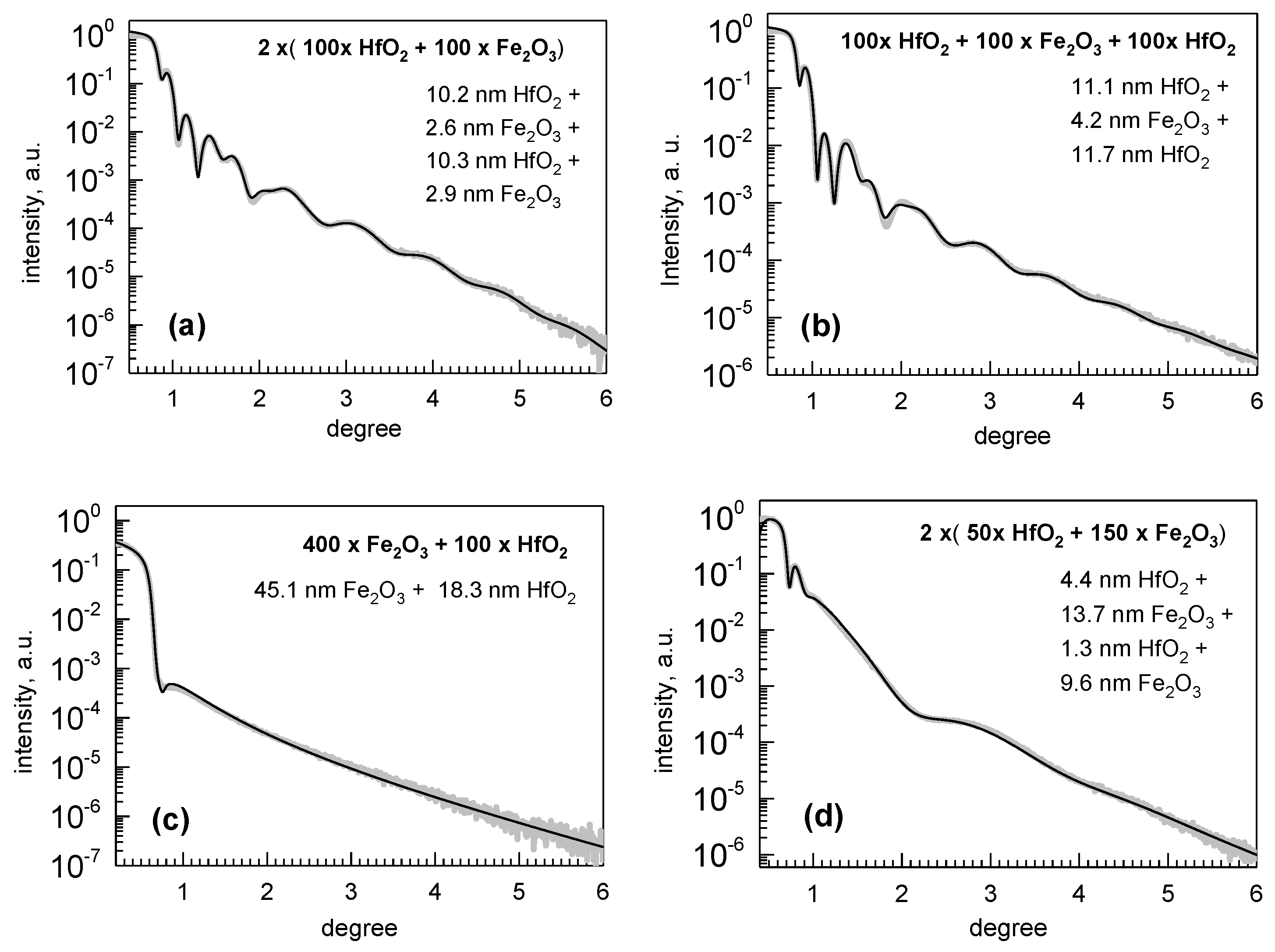
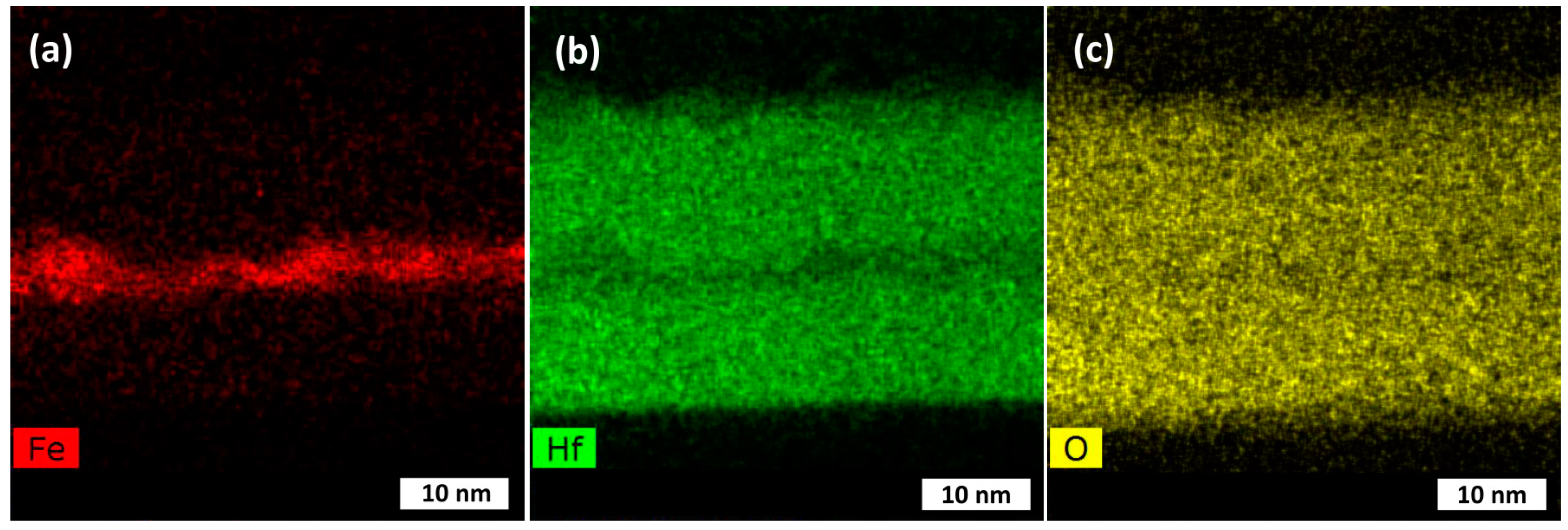
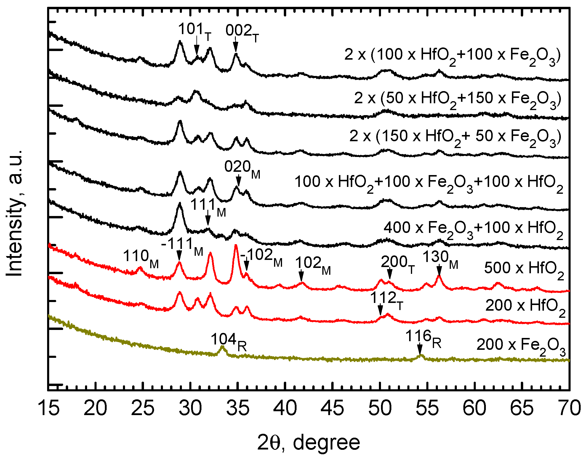
3.1. Growth and Structure

The metal oxide films constituting the nanolaminates were grown in processes under the same reactor conditions and exploiting the same precursor chemistry as those earlier suited to the growth of HfO2 [34] and Fe2O3 [35] films. In the present study, the thickness of multilayered HfO2-Fe2O3 films could be appreciably well controlled by adjusting the amounts of the growth cycles for constituent oxide layers (Table 1). In addition, the presence of iron and hafnium in the films was proven by both XRF and EDS analysis, whereby the relative contents of both metals were correlated to the relative amounts of their growth cycles applied (Table 1, Figure 1a). Further, chlorine and carbon were detected as impurities present in the films (Figure 1b). Both impurities can be regarded as natural residues arising from the ligands to the metal precursors. Within the accuracy limits of the analysis method, the content of Cl and C was not systematically dependent on the relative deposition cycle ratio.
The HfO2-Fe2O3 multilayers were truly formed as nanolaminates, as proven by XRR results depicted in Figure 2. The X-ray reflection intensity curves allowed one to fit the measured data, in a good approximation, with the predicted thicknesses of the constituent layers of both metal oxides, roughly correlated to the amounts of deposition cycles applied in the case of both HfO2 and Fe2O3. It is well known that in the case of ALD, the growth rates of materials on substrates of foreign composition may markedly differ at different growth stages, generally being essentially lower at the early stages of growth, i.e., at low thicknesses. The influence of the nucleation rate and the length of the so-called incubation period depends on temperature, substrate, and growing material, and should be explored separately, if required. In the present study, the growth rate of HfO2 on Fe2O3 noticeably exceeded the growth rate of Fe2O3 on HfO2. In the case of the growth of HfO2 on crystallized Fe2O3 (Figure 2c), the growth rate of HfO2 could reach as high as 0.18 nm/cycle, possibly supported by a larger specific surface area of underlying polycrystalline iron oxide layer.
STEM studies revealed sequential deposition of the hafnium and iron oxide layers, distinct in terms of structure (Figure 3) and elemental distribution (Figure 4), thus supporting the XRR results. One can see that the layers were crystallized throughout the film thickness (Figure 3a,b) without structurally sharp interfaces between the HfO2 and Fe2O3 constituent layers, still enabling the distinction between metal oxides due to the differences in atomic numbers. At the same time, the interface between HfO2 and the amorphous SiO2 top layer on the Si substrate was sharply formed and distinct (Figure 3c). It is, however, to be noted that the growth rates and resulting thicknesses of component layers in nanolaminate structures are not to be compared to those of reference films. It is well-known that the films grown by ALD require an incubation time before achieving stable growth and structural formation. The length of the incubation period may vary considerably, depending on the material to be grown as well as the substrate material and structure. Nucleation at early stages, i.e., growth of HfO2 on Fe2O3 and vice versa would require a separate study. Compositionally, the constituent layers became clearly distinguishable (Figure 4), allowing one to rely on the formation of nanomaterial composed of physically and chemically different oxides, further enabling the appearance of both magnetic and insulating materials’ properties.
The Fe2O3 films grown alone without alternate layering with HfO2 were moderately crystallized in their as-deposited states (Figure 5, the bottom pattern). Two weak but still distinct reflection peaks at 33.6 and 56.5° could be attributed to the 104 and 116 reflections of rhombohedral Fe2O3, that is, the hematite phase. At the same time, the HfO2 films grown alone without alternate layering with Fe2O3 were relatively more crystallized in their as-deposited states (Figure 5, the 2nd pattern from bottom). The HfO2 film grown using 200 deposition cycles could be described as a multiphase solid medium consisting of a stable monoclinic phase of HfO2 and a metastable, quite likely tetragonal, polymorph of HfO2. Whereas most of the reflection peaks remained very weak, the most distinct reflections unambiguously belonging to the −111 and 111 of monoclinic HfO2 peaked at 28.3 and 31.5°, respectively. Between the latter reflections, a peak assigned as 101 of tetragonal HfO2 was clearly detected at 30.3°. These three neighboring reflections can be regarded as proof of multiphase composition. Further and notably, after 500 ALD cycles, the metastable phases, if initially formed and present in HfO2 films, were already almost insignificant in the diffraction patterns. The diffractogram from the HfO2 film grown using 500 cycles comprised reflections attributed exclusively to monoclinic HfO2 (Figure 5, the 3rd pattern from bottom).
Somewhat surprisingly, in the diffractograms taken from most of the films consisting of stacked HfO2 and Fe2O3 layers, no reflections attributable to any of the known iron oxide phases could be recognized. At the same time, crystallization in the films was obvious and due to the crystal growth in the HfO2 corresponding to the stacks or multilayers. With regard to the reflections characteristic of HfO2, the significance of the ones attributable to −111 and 111 of monoclinic HfO2, peaking at 28.3 and 31.5°, respectively, tended to increase with the relative amounts of HfO2 deposition cycles (Figure 5). The relative significance of the reflection assigned as 101 of tetragonal HfO2, at 30.3°, quite expectedly increased with the decrease in the relative amount of the HfO2 deposition cycles (Figure 5). Notably, reflections characteristic of Fe2O3 did not appear in the stacked HfO2 and Fe2O3 layers, with an exception of the sample grown using the cycle sequence of 400 × Fe2O3 + 100 × HfO2, where a weak 104 peak of rhombohedral hematite phase could be recognized at 33.5°.

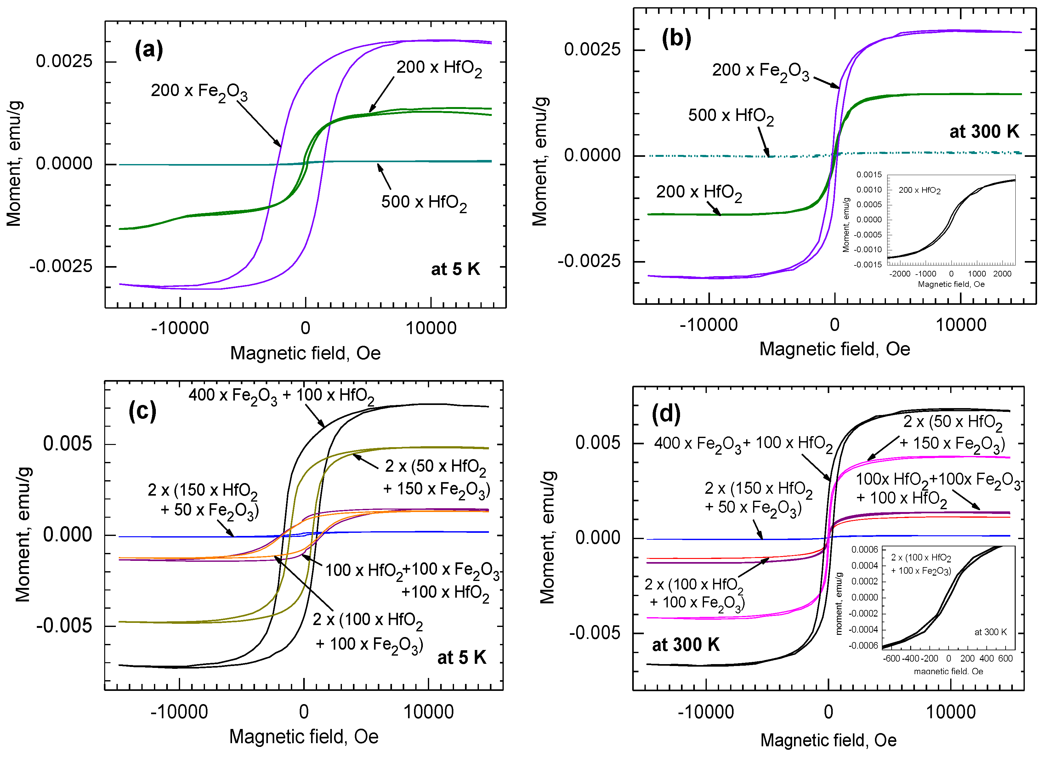
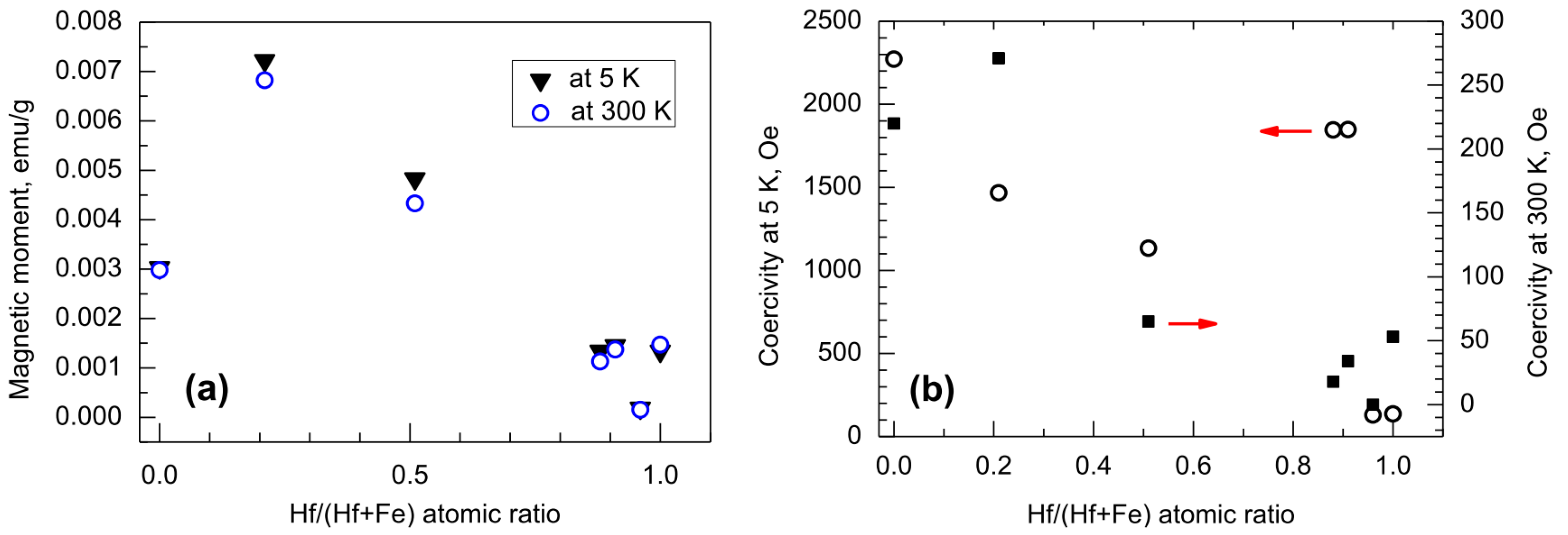
3.2. Magnetization Behavior

The reference Fe2O3 film grown on diamagnetic Si substrates expectedly demonstrated ferromagnetic-like magnetization behavior (Figure 6a) with the coercive force measured as strong as 2272 Oe at 5 K. The thinnest 24 nm-thick HfO2 films grown in the present study using 200 ALD cycles were magnetized nonlinearly and saturatively in external fields (Figure 6a). Both the saturation magnetization and the coercive field remained low, although clearly measurable, in the 24 nm-thick HfO2 film compared to those of the Fe2O3 films. At the same time, the saturation magnetization and coercivity in the 54 nm-thick HfO2, grown using 500 cycles, became suppressed almost entirely. This is plausibly due to the obvious difference between phase compositions of 24 and 54 nm-thick HfO2 films (Figure 5). The thinner HfO2 film contained, besides stoichiometric monoclinic HfO2, probably also oxygen-deficient metastable either tetragonal or cubic HfO2, which would give rise to the magnetization. Upon an increase in the film thickness and crystal growth, the formation of dominant monoclinic dioxide caused a suppression of the magnetization in the solid material. At room temperature, the saturation magnetization values were not significantly decreased, differently from coercitivities. Upon increasing the measurement temperatures from 5 to 300 K, the coercivities were decreased nearly 10, 4, and 2 times in the Fe2O3 film grown using 200 and 500 cycles, and in HfO2 film grown using 200 cycles, respectively (Figure 6b)
With regard to the HfO2 films, undoped and crystallized hafnium dioxide is not supposed to magnetize in its bulk and stoichiometric form, and contamination by handling with stainless-steel tweezers may sometimes have led to measurable magnetic signals [36]. However, magnetization earlier unexpectedly detected in HfO2 films [37] can intentionally be induced, as supported by the presence of defects, in the first place oxygen vacancies [19,20]. Oxygen vacancies are inevitable constituents in the metal oxide lattices, also considered as a cause of the filamentary switching mechanism [38,39,40] in the device cells.
In the samples in which Fe2O3 and HfO2 films were grown into double, triple, or four-layered stacks, the saturation magnetization values obtained at both 5 and 300 K tended, somewhat expectedly, to be the highest in the samples where the amount of sequential Fe2O3 growth cycles exceeded those applied for the HfO2 by 3–5 times (Figure 6c). However, in the case of laminated films, one should take into account that the microstructure of the individual Fe2O3 layers, most strongly affecting the magnetic properties, also varies due to the thickness variation (Figure 2). For instance, in the double-layered (400 × Fe2O3 + 100 × HfO2) sample, the Fe2O3 was moderately crystallized, whereas in all other laminated samples, Fe2O3 was X-ray-amorphous (Figure 5). Notably, the thickness of Fe2O3 in the double layer was nearly 10 times higher compared to that in the three- and four-layer samples when 100 cycles of Fe2O3 was applied (see Figure 2a,b). Apparently, in the latter samples, smaller Fe2O3 nanocrystals could form and possibly agglomerate. The coercivity value measured at 5 K for the film consisting of two double layers of HfO2 and Fe2O3 grown using 50 and 150 cycles, respectively, exceeded 1100 Oe. Coercivity in the double layer consisting of a Fe2O3 film grown at first using 400 cycles, followed by HfO2 grown using 100 cycles, reached nearly 1500 Oe. At room temperature, these values were decreased down to 65 and 271 Oe, respectively.
Despite the ability of nanocrystalline HfO2 to moderately magnetize, also revealing hysteretic performance, the magnetization in terms of both saturation and coercive force was quite naturally dominated by Fe2O3 constituting the nanolaminates. Higher amounts of iron in the iron-hafnium oxide multilayers certainly caused increments in both saturation magnetization (Figure 7a) and coercivity (Figure 7b). Interestingly, relatively strong coercivities among nanolaminate samples, reaching nearly 1850 Oe at 5 K and remaining below 50 Oe at 300 K, were obtained in the triple HfO2-Fe2O3-HfO2 layer and in four-layer film consisting of two HfO2-Fe2O3 double layers (Figure 6c). These samples were characterized by Hf/(Hf + Fe) ratios of 0.91 and 0.88, respectively (Figure 7b, Table 1). In the latter two samples, all the constituent metal oxide layers were grown using 100 ALD cycles. At the same time, the saturation magnetization in the same samples was decreased about five times below the values characterizing the films containing Fe2O3 layers grown using 150 and 400 cycles, described above. It is thus possible that despite the relatively low Fe2O3 amount in such laminates and accompanying weak saturation magnetization, the growth of constituent oxides in such nanolaminates after application of sufficient amounts of deposition cycles has enabled the ordering and growth of nanocrystals enhancing structure or shape anisotropy and a simultaneous increment in coercivity. Further and more detailed studies including parametrization and scaling up the process would be required in order to clarify the interdependencies between deposition cycle numbers, crystallographic orientation, and magnetic performance.
The samples based on triple HfO2-Fe2O3-HfO2-layer and four-layer film consisting of two HfO2-Fe2O3 double layers are those worth further attention, because the same samples further exhibited defined resistive switching behavior, as will be described below. Superparamagnetic behavior was expected at first, and the same samples were additionally subjected to the temperature-dependent magnetization measurements. As was already implied by the magnetization-field curves recorded at 5 and 300 K (Figure 6c,d), the triple-layered film grown using the cycle sequence of 100 × HfO2 + 100 × Fe2O3 + 100 × HfO2 exhibited slightly higher saturation magnetization values compared to the four-layered film grown using the cycle sequence of 2 × (100 × HfO2 + 100 × Fe2O3). This can plausibly be explained by the distribution of Fe2O3 differing in the latter two samples. In the four-layered sample, the thickness of the two Fe2O3 layers summarized was similar to that in the three-layer sample containing a single Fe2O3 layer in between two HfO2 layers (Figure 2). Therefore, in the three-layer sample, the short-range order in Fe2O3, although not detectable by GIXRD, could possibly be better defined compared to that in the four-layer film, providing higher saturation magnetization. Further, field-cooling (FC) measurements were carried out in the temperature range of 355–5 K (Figure 8), recording the magnetization values at each temperature after the application of the external field of 1000 Oe. For both samples, the zero-field-cooling (ZFC) measurements were also carried out in order to estimate the blocking temperatures related to thermal energy, below which the magnetization in a material consisting of single-domain nanocrystallites would lose its preferred direction in a near-zero external field and relax. In the four-layer structure (Figure 8a), the blocking temperature, TB, remained lower compared to that estimated for the three-layer structure (135 vs. 215 K, Figure 8b). This may be indicative of the effect of the lower amount of easily magnetized, and for this reason, also more easily reoriented, amount of iron-rich nanoparticles present in the three-layer film.

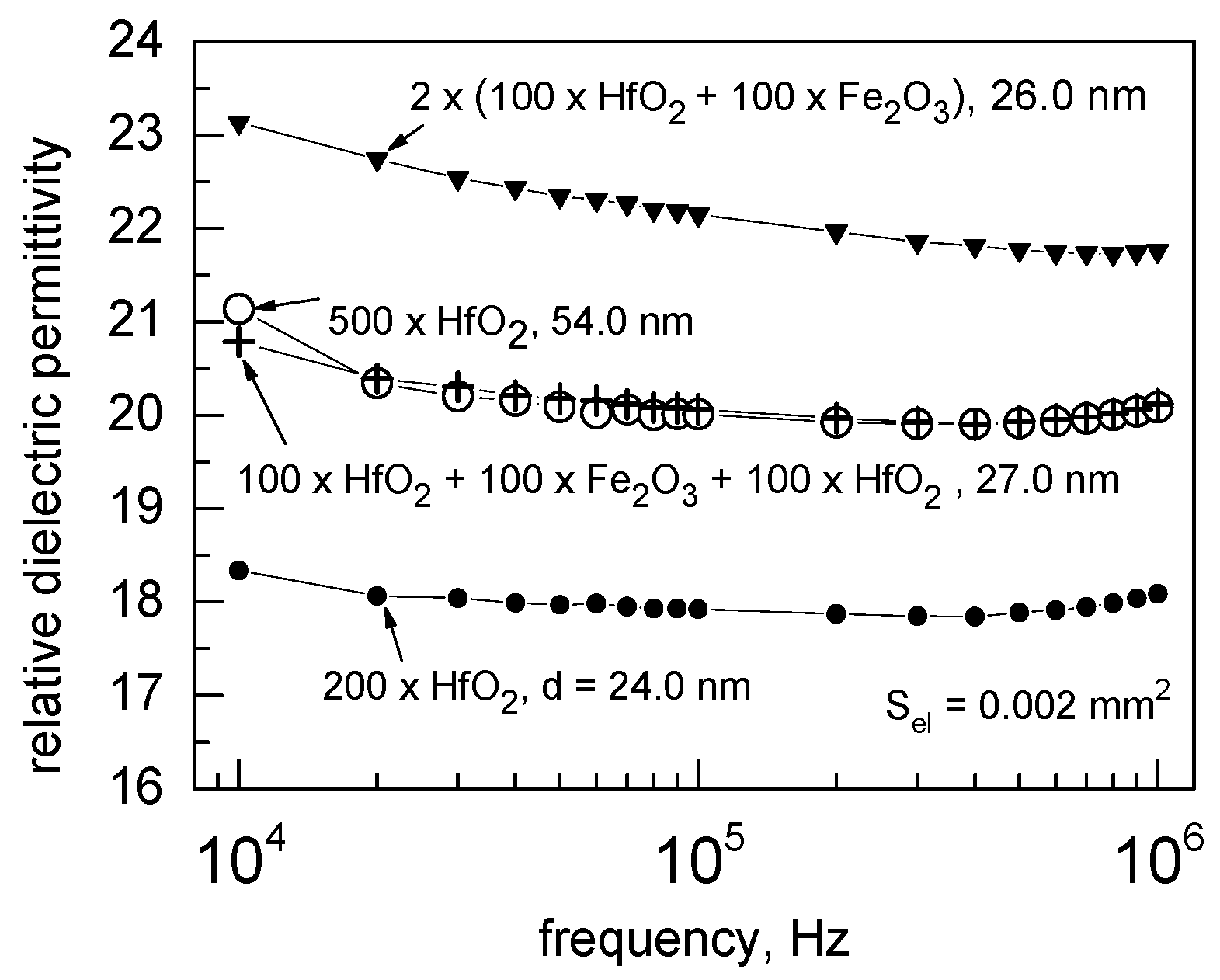
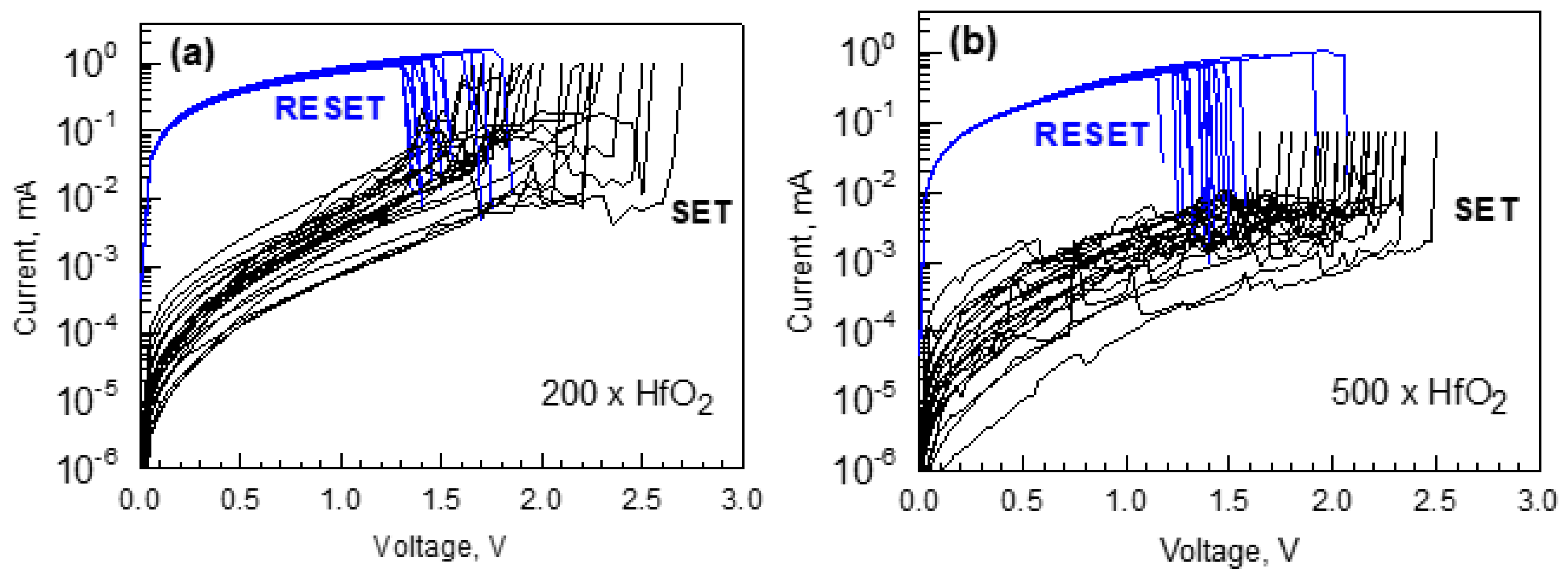
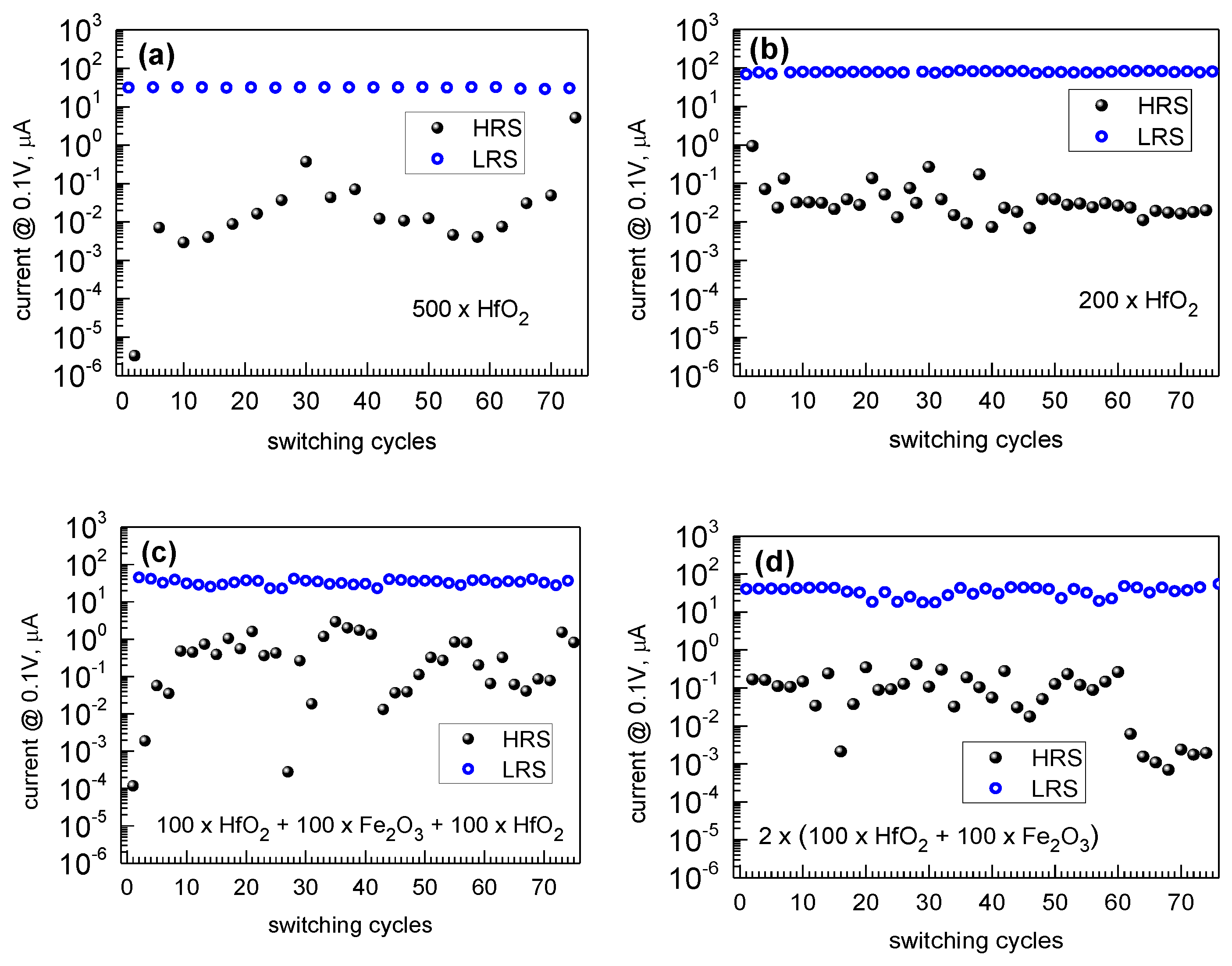
3.3. Electrical Behavior

The reference HfO2 films behaved electrically as dielectric materials with defined insulating properties. Figure 9 represents the results of capacitance dispersion measurements, expressed as permittivity-frequency curves, after calculating the permittivity considering the simple parallel-plate capacitor configuration, containing dielectric film with thickness determined by XRR measurements. One can see that the permittivity-frequency dependencies represent appreciably flat plateaus, being indicative of the minor role for parasitic space charge and interfacial polarization in the frequency range of 10 kHz–1 MHz. The average permittivity value for the 24 nm-thick HfO2 film grown using 200 deposition cycles remained at 18, whereas the permittivity of the 54 nm-thick film grown using 500 cycles exceeded 20. This difference was plausibly due to the more developed crystallinity in the thicker film. Since the HfO2 films in the present study were characterized with multiphase composition (Figure 5), i.e., contained both metastable and stable polymorphs of HfO2, the permittivity value remained even, quite expectedly, between those earlier calculated as those characteristic of corresponding phases [41]. One could also note that the permittivity values measured in the present study corresponded appreciably well to those measured earlier in a study reporting insulating properties of HfO2-based nanolaminates and single HfO2 films grown by ALD using HfCl4 and H2O as precursors [42].
The HfO2-Fe2O3-HfO2 triple layer and the periodically deposited sample consisting of two HfO2-Fe2O3 double layers grown using 100 deposition cycles for each component oxide behaved electrically reliable enough to enable stable capacitance measurements. The capacitance, and consequently the estimated permittivity values, appeared higher than those in the reference HfO2 film grown to the comparable thickness (Figure 9), possibly due to the influence of interfacial polarization enabled by the relatively leaky intermediate Fe2O3 layers. Furthermore, even the iron-rich sample consisting of periodical nanolaminate deposited using the cycle sequence of 2 × (50 × HfO2 + 150 × Fe2O3) film grown to the total thickness of 29 nm occurred electrically stable enough, exhibiting permittivity values up to 50–60 (not shown) in the frequency range examined. Iron oxide films, deposited without complementary HfO2 layers, could not be capacitively evaluated due to their high conductivity. One could clearly see that alternate layering of HfO2 and Fe2O3 usefully assisted the trade-off between conductivity and capacitance increments, being indicative of the possibility to usefully tune the electrical resistivity in magnetic materials. The reliability of capacitance measurements, revealing the permittivity of the artificially structured HfO2-Fe2O3 laminates, evidently governed by the properties of HfO2, allows one to further expect stability of the resistive switching phenomena.
The HfO2 reference films grown to the thicknesses of 24 and 54 nm after application of 200 and 500 deposition cycles, respectively, exhibited well-defined unipolar resistive switching behavior (Figure 10). The main RS parameters, such as low to high resistive state ratios and switching voltages, did not differ markedly for the films grown to different thicknesses, being indicative of the insensitivity of the polymorphic phase composition differing in these HfO2 films (Figure 5). Switching parameters did not depend on the device area in those samples in which both 0.002 mm2 and 0.052 mm2 electrode surface areas delivered RS behavior. In the case of the HfO2 films grown to the thickness of 54 nm, reliable switching behavior could be observed only upon measurements conducted on the electrodes of the smallest size, 0.002 mm2 (Figure 10b), whereas in the case of the HfO2 films grown to the thickness of 24 nm, electrodes with an area of 0.052 mm2 also allowed one to acquire reliable switching characteristics (Figure 10a). Plausibly, growing film thickness enables the growth of larger crystallites accompanied by higher surface roughness, structural inhomogeneities, and voids, necessitating measurements on smaller sized electrodes in order to acquire reliable results. One has to note that an apparent dependence of switching reliability on electrode area is not necessarily to be related to the domination of the interfacial conduction mechanism over the filamentary one. Indeed, the unipolar switching produced by the thermochemical mechanism (TCM) is known to be filamentary [14,43], and the switching parameters, i.e., resistance in both the LRS and HRS as well as current values, are expected to be independent from the electrode area [14,44,45,46]. Under this thermochemical mechanism, thermochemical redox processes dominate the electrochemical ones. Local redox reactions occur due to a local temperature increase that energetically favors lower oxidation states. Thus, oxygen drifts out of this high-temperature region, producing a variation of the local conductivity due to stoichiometry variations, which are usually attributed to the formation of a lower oxidation state sub-oxide, or the metal itself if such sub-oxide does not exist [15,47]. The filaments can then be induced under the chosen voltage polarity and disrupted afterwards by the currents causing Joule heating, healing the defective channel under an applied voltage of the same polarity, but inducing much higher currents in the low resistivity state. As it is common in cells presenting unipolar resistive switching, the low to high resistivity state ratios could exceed three orders of magnitude, with a high cycle-to-cycle variability of the switching voltages and the resistance value of the HRS.
Figure 11 demonstrates defined switching behavior recorded in periodical HfO2-Fe2O3 laminates (Figure 11a,b) as well as in the HfO2-Fe2O3-HfO2 triple-layer stack (Figure 11c). It is worth noting that in the periodically stacked HfO2-Fe2O3 laminate grown using the cycle sequence of 2 × (150 × HfO2 + 50 × Fe2O3), the low to high resistivity state ratios could reach even five orders of magnitude (Figure 11a). However, the repeatability of switching cycles in such films remained rather low, not allowing one to reliably record more than 8–10 switching cycles. To additionally recall, this sample was relatively weakly magnetized (Figure 6c,d and Figure 7), demonstrating almost insignificant saturation magnetization and rather weak coercitivity (below 200 Oe) already at 5 K compared to the rest of the samples grown using higher relative amounts of Fe2O3 deposition cycles. Thus, the deposition program applied to this particular sample could result in a material representing trade-off between magnetic and resistively switching performance, implying a possibility for optimization.
The repeatability of current-voltage behavior upon resistive switching cycles after endurance tests was obvious in the reference HfO2 films (Figure 12a,b). However, noticeable scattering in the current values in high-resistance states upon sequential switching cycles was recorded. One could suppose that the stability of switching the current level in the HRS after the RESET events is markedly dependent of the structural quality of the material restored after breaking filaments or quenching the conduction channels. At the same time, the resistivity levels in LRS after SET events might more significantly be determined by the current compliance limits. In this regard, the stability of HRS could serve as a structure-related descriptor of the crystalline switching medium and be worth depicting as an implication of the device functionality.
The decrement in the low to high resistivity ratio was detected simultaneously with increased variability in low resistivity states. The LRS:HRS ratios during endurance tests remained slightly higher and also somewhat more stable in the reference HfO2 films (Figure 12a,b) compared to the results recorded in a device built on triple-layered HfO2-Fe2O3-HfO2 film (Figure 12c) as well as on four-layered HfO2-Fe2O3-HfO2-Fe2O3 (Figure 12d), all grown to comparable thicknesses. The increased variability in the LRS is most plausibly due to the iron oxide constituents in the films, increasing the material conductivity already in its virgin state before the SET event. This property may ease the formation of conductive channel but worsen the control over breaking it. The main outcome of the RS measurements was, thus, the recognition of a certain balance between growth cycles of constituent dielectric and magnetic materials while engineering the deposition process, before the achievement of both resistive switching and magnetic polarization at room temperature.
It should be emphasized that the unipolar resistive switching behavior of these samples has been of high interest when studying the physics behind RS. Although previous studies on HfO2-based RRAM devices have also shown unipolar resistive switching, it was in some way always due to the metals chosen for the bottom and top electrodes [48]. It is known that RRAM cells that use the same metal for both electrodes will most likely show URS [13], as observed in the case of Pt/HfO2/Pt [49,50] and TiN/HfO2/TiN [51] MIM stacks. At the same time, Pt/HfO2/TiN cells can demonstrate both URS and BRS [52,53]. Pt/HfO2/Ti stacks have also shown bipolar switching [49], indicating better properties of Ti as an oxygen reservoir when compared to TiN, enabling and supporting the VCM. Thus, the use of a thin Ti cap in TiN/HfO2/Ti/TiN devices allows one to observe BRS [54], with unipolar switching appearing only under extreme programming conditions [55]. When looking at RRAM cells similar to the ones presented in this work, i.e., HfO2-based RRAM with TiN and Ti as bottom and top electrodes (BE an TE), respectively, the literature strongly suggests that bipolar switching is expected [48,49,50], contrary to the results presented here. This could be attributed to the use of Au as the top electrode over to Ti. Bertaud et al. [56] showed that the use of a metal with low a enthalpy of formation of oxides, such as gold, for the TE, should lead to unipolar switching, and Walzcyk et al. [57] reported URS in Au/HfO2/TiN MIM stacks. Here, it is worth noting that a previous work on resistively switching media based on Fe2O3 has also reported URS [58], although their stack made use of somewhat symmetric Pt metal electrodes (Pt/Fe2O3/Pt/Ti). Nevertheless, a study conducted as early as 1969 [59] reports unipolar switching in thin iron oxide, associating increased conductivity (forming or SET processes) either with the formation of sub-oxides mentioned above [47] or with the expected decrease in transition metals’ resistance with increasing temperature, known as metal-insulator transitions [60], which has been specifically proven for both thick [61] and thin Fe2O3 films [62].

4. Summary and Conclusions

Insulating HfO2 and magnetic Fe2O3 were successfully tailored as nanolaminates of alternately layered films of hafnium and iron oxides. The relative contents of hafnium and iron were modified by changing the relative amounts of the deposition cycles for both constituent oxides. The films contained some amounts of chlorine and carbon as residual impurities. The structure of the films could be regarded as nanocrystalline, whereby a multiphase nature of nanolaminates, based on the simultaneous appearance of both stable and metastable polymorphs of HfO2, was established.
Stable dielectric polarization and resistive switching properties expectedly characteristic of HfO2 were achieved and recorded in the laminated stacks containing measurable amounts of relatively highly conducting Fe2O3. At the same time, the presence of Fe2O3 as well as formation of nanocrystalline phases of HfO2 enabled the appearance and recording of nonlinear, saturative, and hysteretic magnetization in the laminates, somewhat correlated with the relative content of Fe2O3. The coercivity appeared the strongest in the films consisting of two sequentially grown HfO2-Fe2O3 double layers as well as a triple HfO2-Fe2O3-HfO2 layer, measured at 5 K. The coercivity diminished drastically at room temperature, remaining, however, measurable below 100 Oe. Notably, the same structures, clearly also exhibited an ability to switch resistively, whereas samples containing relatively larger amounts of iron could not switch resistively due to increasing conductivity.
All samples deposited using 100 or less Fe2O3 cycles between HfO2 layers demonstrated unipolar resistive switching. Higher amounts of Fe2O3 ALD cycles resulted in a decrease of the low to high resistance state ratio. Fe2O3 layers constituting the laminates probably did not allow for the formation of conductive filaments as efficiently as HfO2, hindering the variability of the low resistance state. The appearance of the unipolar resistive switching of these samples may be regarded as notable in light of common knowledge suggesting that Ti and TiN used for the top and bottom electrodes, mounting HfO2, should lead to bipolar resistive switching. This could be due to the dominance of a thermochemical process over an electrochemical one. Further studies could be devoted to the investigation of the effect of electrodes with variable enthalpy as well as coupling between conductivity and electromagnetic polarization.

Author Contributions

Conceptualization, K.K. (Kristjan Kalam) and K.K. (Kaupo Kukli); methodology, K.K. (Kristjan Kalam); software, G.V., J.L., J.M.L., R.R. and M.O.; formal analysis, G.V., J.L., R.R. and A.T. (Aivar Tarre); investigation, R.R., G.V., J.M.L., M.O., A.K. and J.K.; resources, R.S., S.D., H.C., A.T. (Aile Tamm) and K.K. (Kaupo Kukli); writing—original draft preparation, K.K. (Kristjan Kalam), K.K. (Kaupo Kukli), G.V. and J.L.; visualization, G.V. and A.T. (Aivar Tarre); project administration, K.K. (Kaupo Kukli), A.T. (Aile Tamm), S.D. and H.C.; funding acquisition, K.K. (Kaupo Kukli), A.T. (Aile Tamm), R.S. and H.C. All authors have read and agreed to the published version of the manuscript.

Funding

The present study was partially supported by the European Regional Development Fund project “Emerging orders in quantum and nanomaterials” (TK134), the Spanish Ministry of Economy and Competitiveness (TEC2017-84321-C4-2-R) with the support of Feder Funds, and the Estonian Research Agency (PRG753, PRG4).

Data Availability Statement

Not applicable.

Conflicts of Interest

The authors declare no conflict of interest. The funders had no role in the design of the study; in the collection, analyses, or interpretation of data; in the writing of the manuscript, or in the decision to publish the results.

References

  1. Wolf, S.A.; Awschalom, D.D.; Buhrman, R.A.; Daughton, J.M.; von Molnár, S.; Roukes, M.L.; Chtchelkanova, A.Y.; Treger, D.M. Spintronics: A spin-based electronics vision for the future. Science 2001, 294, 1488–1495. [Google Scholar] [CrossRef] [PubMed] [Green Version]
  2. Waser, R.; Aono, M. Nanoionics-based resistive switching memories. Nat. Mater. 2007, 6, 833–840. [Google Scholar] [CrossRef] [PubMed]
  3. Li, S.-S.; Su, Y.-K. Conductive filaments controlled ferromagnetism in Co-doped ZnO resistive switching memory device. Jpn. J. Appl. Phys. 2019, 58, SBBI01. [Google Scholar] [CrossRef]
  4. Du, F.; Li, Y.; Li, X.; Yang, J.; Bai, Y.; Quan, Z.; Liu, C.; Xu, X. Resistive switching and its modulating ferromagnetism and magnetoresistance of a ZnO:Co/SiO2:Co film. J. Magn. Magn. Mater. 2019, 489, 165445. [Google Scholar] [CrossRef]
  5. Xie, J.; Ren, S.; Bu, J.; Cheng, B.; Liu, W.; Liu, L.; Zhou, G.; Qin, H.; Hu, J. Resistive switching and ferromagnetism modulation in copper oxide film on Nb:SrTiO3 substrate. J. Magn. Magn. Mater. 2018, 465, 295–299. [Google Scholar] [CrossRef]
  6. Ren, S.; Zhu, G.; Xie, J.; Bu, J.; Qin, H.; Hu, J. Resistive switching and electrical control of ferromagnetism in a Ag/HfO2/Nb:SrTiO3/Ag resistive random access memory (RRAM) device at room temperature. J. Phys. Condens. Matter 2016, 28, 056001. [Google Scholar] [CrossRef] [PubMed]
  7. Slesazeck, S.; Mikolajick, T. Nanoscale resistive switching memory devices: A review. Nanotechnology 2019, 30, 352003. [Google Scholar] [CrossRef] [PubMed]
  8. Chen, A. A review of emerging non-volatile memory (NVM) technologies and applications. Solid-State Electr. 2016, 125, 25–38. [Google Scholar] [CrossRef]
  9. Jasmin, A.C. Filamentary model in resistive switching materials. AIP Conf. Proc. 2017, 1901, 060004. [Google Scholar] [CrossRef]
  10. Waser, R. Redox-based resistive switching memories. J. Nanosci. Nanotech. 2012, 12, 7628–7640. [Google Scholar] [CrossRef] [Green Version]
  11. Menzel, S.; Waters, M.; Marchewka, A.; Böttger, U.; Dittmann, R.; Waser, R. Origin of the ultra-nonlinear switching kinetics in oxide-based resistive switches. Adv. Funct. Mater. 2011, 21, 4487–4492. [Google Scholar] [CrossRef]
  12. Valov, I. Redox-based resistive switching memories (ReRAMs): Electrochemical systems at the atomic scale. Chem. Electro. Chem. 2014, 1, 26–36. [Google Scholar] [CrossRef]
  13. Valov, I. Interfacial interactions and their impact on redox-based resistive switching memories (ReRAMs). Semicond. Sci. Technol. 2017, 32, 093006. [Google Scholar] [CrossRef]
  14. Ielmini, D.; Bruchhaus, R.; Waser, R. Thermochemical resistive switching: Materials, mechanisms, and scaling projections. Phase Trans. 2011, 84, 570–602. [Google Scholar] [CrossRef]
  15. Waser, R. Electrochemical and thermochemical memories. In Proceedings of the 2008 IEEE International Electron Devices Meeting, San Francisco, CA, USA, 15–17 December 2008. [Google Scholar] [CrossRef]
  16. Bersuker, G.; Gilmer, D.C.; Veksler, D.; Kirsch, P.; Vandelli, L.; Padovani, A.; Larcher, L.; McKenna, K.; Shluger, A.; Iglesias, V.; et al. Metal oxide resistive memory switching mechanism based on conductive filament properties. J. Appl. Phys. 2011, 110, 124518. [Google Scholar] [CrossRef]
  17. Lin, K.-L.; Hou, T.-H.; Shieh, J.; Lin, J.-H.; Chou, C.-T.; Lee, Y.-J. Electrode dependence of filament formation in HfO2 resistive-switching memory. J. Appl. Phys. 2011, 109, 084104. [Google Scholar] [CrossRef] [Green Version]
  18. Maldonado, D.; Roldán, A.M.; González, M.B.; Jiménez-Molinos, F.; Campabadal, F.; Roldán, J.B. Influence of magnetic field on the operation of TiN/Ti/HfO2/W resistive memories. Microel. Eng. 2019, 215, 110983. [Google Scholar] [CrossRef] [Green Version]
  19. Hong, N.H. Magnetism due to defects/oxygen vacancies in HfO2 thin films. Phys. Stat. Sol. c 2007, 4, 1270–1275. [Google Scholar] [CrossRef]
  20. Tereshchenko, O.E.; Golyashov, V.A.; Eremeev, S.V.; Maurin, I.; Bakulin, A.V.; Kulkova, S.E.; Aksenov, M.S.; Preobrazhenskii, V.V.; Putyato, M.A.; Semyagin, B.R.; et al. Ferromagnetic HfO2/Si/GaAs interface for spin-polarimetry applications. Appl. Phys. Lett. 2015, 107, 123506. [Google Scholar] [CrossRef]
  21. Singh, R. Unexpected magnetism in nanomaterials. J. Mag. Mag. Mater. 2013, 346, 58–73. [Google Scholar] [CrossRef]
  22. Daub, M.; Bachmann, J.; Jing, J.; Knez, M.; Gösele, U.; Barth, S.; Mathur, S.; Escrig, J.; Altbir, D.; Nielsch, K. Ferromagnetic nanostructures by atomic layer deposition: From thin films towards core-shell nanotubes. ECS Trans. 2007, 11, 139–148. [Google Scholar] [CrossRef] [Green Version]
  23. Schneider, J.R.; Baker, J.G.; Bent, S.F. The influence of ozone: Superstoichiometric oxygen in atomic layer deposition of Fe2O3 using tert-butylferrocene and O3. Adv. Mater. Interfaces 2020, 7, 2000318. [Google Scholar] [CrossRef]
  24. Márquez, P.; Alburquenque, D.; Celis, F.; Freire, R.M.; Escrig, J. Structural, morphological and magnetic properties of iron oxide thin films obtained by atomic layer deposition as a function of their thickness. J. Magn. Magn. Mater. 2021, 530, 167914. [Google Scholar] [CrossRef]
  25. Štefanić, G.; Musić, S. Thermal behavior of the amorphous precursors of the Fe2O3-HfO2 system. Thermochim. Acta 2001, 373, 59–67. [Google Scholar] [CrossRef]
  26. Rao, M.S.R.; Kundaliya, D.C.; Dhar, S.; Cardoso, C.A.; Curtin, A.; Welz, S.J.; Erni, R.; Browning, N.D.; Lofland, S.E.; Metting, C.J.; et al. Search for magnetism in Co and Fe doped HfO2 thin films for potential spintronic applications. Mater. Res. Soc. Proc. 2004, 830, 262–275. [Google Scholar] [CrossRef]
  27. Kukli, K.; Kemell, M.; Castán, H.; Dueñas, S.; Seemen, H.; Rähn, M.; Link, J.; Stern, R.; Ritala, M.; Leskelä, M. Atomic layer deposition and properties of HfO2-Al2O3 nanolaminates. ECS J. Solid State Sci. Tech. 2018, 7, P501–P508. [Google Scholar] [CrossRef] [Green Version]
  28. Kalam, K.; Seemen, H.; Mikkor, M.; Ritslaid, P.; Stern, R.; Dueñas, S.; Castán, H.; Tamm, A.; Kukli, K. Electric and magnetic properties of atomic layer deposited ZrO2-HfO2 thin films. ECS J. Solid State Sci. Technol. 2018, 7, N117–N122. [Google Scholar] [CrossRef]
  29. Ossorio, O.G.; Dueñas, S.; Castán, H.; Tamm, A.; Kalam, K.; Seemen, H.; Kukli, K. Resistive switching properties of atomic layer deposited ZrO2-HfO2 thin films. In Proceedings of the 2018 Spanish Conference on Electron Devices (CDE), Salamanca, Spain, 14–16 November 2018. [Google Scholar] [CrossRef]
  30. Kukli, K.; Kemell, M.; Castán, H.; Dueñas, S.; Link, J.; Stern, R.; Heikkilä, M.J.; Jõgiaas, T.; Kozlova, J.; Rähn, M.; et al. Magnetic properties and resistive switching in mixture films and nanolaminates consisting of iron and silicon oxides grown by atomic layer deposition. J. Vac. Sci. Technol. A 2020, 38, 042405. [Google Scholar] [CrossRef]
  31. Arroval, T.; Aarik, L.; Rammula, R.; Kruusla, V.; Aarik, J. Effect of substrate-enhanced and inhibited growth on atomic layer deposition and properties of aluminum–titanium oxide films. Thin Solid Films 2016, 600, 119–125. [Google Scholar] [CrossRef]
  32. Granneman, E.; Fischer, P.; Pierreux, D.; Terhorst, H.; Zagwijn, P. Batch ALD: Characteristics, comparison with single wafer ALD, and examples. Surf. Coat. Technol. 2017, 201, 8899–8907. [Google Scholar] [CrossRef]
  33. Zagwijn, P.; Verweij, W.; Pierreux, D.; Adjeroud, N.; Bankras, R.; Oosterlaken, E.; Snijders, G.J.; van den Hout, M.; Fischer, P.; Wilhelm, R.; et al. Novel batch titanium nitride CVD process for advanced metal electrodes. ECS Transact. 2008, 13, 459–464. [Google Scholar] [CrossRef] [Green Version]
  34. Aarik, L.; Arroval, T.; Mändar, H.; Rammula, R.; Aarik, J. Influence of oxygen precursors on atomic layer deposition of HfO2 and hafnium-titanium oxide films: Comparison of O3- and H2O-based processes. Appl. Surf. Sci. 2020, 530, 147229. [Google Scholar] [CrossRef]
  35. Kalam, K.; Seemen, H.; Ritslaid, P.; Rähn, M.; Tamm, A.; Kukli, K.; Kasikov, A.; Link, J.; Stern, R.; Dueñas, S.; et al. Atomic layer deposition and properties of ZrO2/Fe2O3 thin films. Beilstein J. Nanotechnol. 2018, 9, 119–128. [Google Scholar] [CrossRef] [PubMed] [Green Version]
  36. Abraham, D.W.; Frank, M.M.; Guha, S. Absence of magnetism in hafnium oxide films. Appl. Phys. Lett. 2005, 87, 252502. [Google Scholar] [CrossRef]
  37. Venkatesan, M.; Fitzgerald, C.B.; Coey, J.M.D. Unexpected magnetism in a dielectric oxide. Nature 2004, 430, 630. [Google Scholar] [CrossRef] [PubMed]
  38. Xue, K.-H.; Miao, X.-S. Oxygen vacancy chain and conductive filament formation in hafnia. J. Appl. Phys. 2018, 123, 161505. [Google Scholar] [CrossRef]
  39. Dai, Y.; Pan, Z.; Wang, F.; Li, X. Oxygen vacancy effects in HfO2-based resistive switching memory: First principle study. AIP Adv. 2016, 6, 085209. [Google Scholar] [CrossRef] [Green Version]
  40. Kumar, S.; Rath, C. Oxygen vacancy mediated stabilization of cubic phase at room temperature and resistive switching effect in Sm- and Dy-doped HfO2 thin film. Phys. Stat. Sol. A 2020, 217, 1900756. [Google Scholar] [CrossRef]
  41. Zhao, X.; Vanderbilt, D. First-principles study of structural, vibrational, and lattice dielectric properties of hafnium oxide. Phys. Rev. B 2002, 65, 233106. [Google Scholar] [CrossRef] [Green Version]
  42. Kukli, K.; Ihanus, J.; Ritala, M.; Leskelä, M. Tailoring the dielectric properties of HfO2–Ta2O5 nanolaminates. Appl. Phys. Lett. 1996, 68, 3737–3739. [Google Scholar] [CrossRef]
  43. Chang, S.H.; Lee, J.S.; Chae, S.C.; Lee, S.B.; Liu, C.; Kahng, B.; Kim, D.-W.; Noh, T.W. Occurrence of both unipolar memory and threshold resistance switching in a NiO film. Phys. Rev. Lett. 2009, 102, 026801. [Google Scholar] [CrossRef] [PubMed]
  44. Baek, I.G.; Lee, M.S.; Seo, S.; Lee, M.J.; Seo, D.H.; Suh, D.-S.; Park, J.C.; Park, S.O.; Kim, H.S.; Yoo, I.K.; et al. Highly scalable nonvolatile resistive memory using simple binary oxide driven by asymmetric unipolar voltage pulses. In Proceedings of the IEDM Technical Digest. IEEE International Electron Devices Meeting, San Francisco, CA, USA, 13–15 December 2004. [Google Scholar] [CrossRef]
  45. Nardi, F.; Ielmini, D.; Cagli, C.; Spiga, S.; Fanciulli, M.; Goux, L.; Wouters, D.J. Sub-10 µA reset in NiO-based resistive switching memory (RRAM) cells. In Proceedings of the 2010 IEEE International Memory Workshop, Seoul, Korea, 16–19 May 2010. [Google Scholar] [CrossRef]
  46. Ielmini, D.; Spiga, S.; Nardi, F.; Cagli, C.; Lamperti, A.; Cianci, E.; Fanciulli, M. Scaling analysis of submicrometer nickel-oxide-based resistive switching memory devices. J. Appl. Phys. 2011, 109, 034506. [Google Scholar] [CrossRef]
  47. Chudnovskii, F.A.; Odynets, L.L.; Pergament, A.L.; Stefanovich, G.B. Electroforming and switching in oxides of transition metals: The role of metal–insulator transition in the switching mechanism. J. Solid State Chem. 1996, 122, 95–99. [Google Scholar] [CrossRef]
  48. Mohammad, B.; Jaoude, M.A.; Kumar, V.; Al Homouz, D.M.; Nahla, H.A.; Al-Qutayri, M.; Christoforou, N. State of the art of metal oxide memristor devices. Nanotechnol. Rev. 2016, 5, 311–329. [Google Scholar] [CrossRef]
  49. Traoré, B.; Xue, K.-H.; Vianello, E.; Molas, G.; Blaise, P.; De Salvo, B.; Padovani, A.; Pirrotta, O.; Larcher, L.; Fonseca, L.R.C.; et al. Investigation of the role of electrodes on the retention performance of HfOx based RRAM cells by experiments, atomistic simulations and device physical modeling. In Proceedings of the 2013 IEEE International Reliability Physics Symposium (IRPS), Monterey, CA, USA, 14–18 April 2013. [Google Scholar] [CrossRef]
  50. Traoré, B.; Blaise, P.; Vianello, E.; Perniola, L.; De Salvo, B.; Nishi, Y. HfO2 based RRAM: Electrode effects, Ti/HfO2 interface, charge injection, and oxygen (O) defects diffusion through experiment and Ab Initio calculations. IEEE Transact. Electron Dev. 2016, 63, 360–368. [Google Scholar] [CrossRef]
  51. Wang, X.P.; Chen, Y.Y.; Pantisano, L.; Goux, L.; Jurczak, M.; Groeseneken, G.; Wouters, D.J. Effect of anodic interface layers on the unipolar switching of HfO2-based resistive RAM. In Proceedings of the 2010 International Symposium on VLSI Technology, System and Application, Hsinchu, Taiwan, 26–28 April 2010. [Google Scholar] [CrossRef]
  52. Goux, L.; Czarnecki, P.; Chen, Y.Y.; Pantisano, L.; Wang, X.P.; Degraeve, R.; Govoreanu, B.; Jurczak, M.; Wouters, D.J.; Altimime, L. Evidences of oxygen-mediated resistive-switching mechanism in TiN\HfO2\Pt cells. Appl. Phys. Lett. 2010, 97, 243509. [Google Scholar] [CrossRef]
  53. Goux, L.; Chen, Y.-Y.; Pantisano, L.; Wang, X.-P.; Groeseneken, G.; Jurczak, M.; Wouters, D.J. On the gradual unipolar and bipolar resistive switching of TiN\HfO2\Pt memory systems. Electrochem. Solid-State Lett. 2010, 13, G54–G56. [Google Scholar] [CrossRef]
  54. Lee, H.Y.; Chen, Y.S.; Chen, P.S.; Wu, T.Y.; Chen, F.; Wang, C.C.; Tzeng, P.J.; Tsai, M.-J.; Lien, C. Low power and nanosecond switching in robust hafnium oxide resistive memory with a thin Ti cap. IEEE Electron. Dev. Lett. 2010, 31, 44–46. [Google Scholar] [CrossRef]
  55. Chen, Y.S.; Lee, H.Y.; Chen, P.S.; Gu, P.Y.; Chen, C.W.; Lin, W.P.; Liu, W.H.; Hsu, Y.Y.; Sheu, S.S.; Chiang, P.C.; et al. Highly scalable hafnium oxide memory with improvements of resistive distribution and read disturb immunity. In Proceedings of the 2009 IEEE International Electron Devices Meeting (IEDM), Baltimore, MD, USA, 7–9 December 2009. [Google Scholar] [CrossRef]
  56. Bertaud, T.; Walczyk, D.; Walczyk, C.; Kubotsch, S.; Sowinska, M.; Schroeder, T.; Wenger, C.; Vallée, C.; Gonon, P.; Mannequin, C.; et al. Resistive switching of HfO2-based metal–insulator–metal diodes: Impact of the top electrode material. Thin Solid Films 2012, 520, 4551–4555. [Google Scholar] [CrossRef]
  57. Walczyk, C.; Wenger, C.; Sohal, R.; Lukosius, M.; Fox, A.; Dąbrowski, J.; Wolansky, D.; Tillack, B.; Müssig, H.-J.; Schroeder, T. Pulse-induced low-power resistive switching in HfO2 metal-insulator-metal diodes for nonvolatile memory applications. J. Appl. Phys. 2009, 105, 114103. [Google Scholar] [CrossRef]
  58. Inoue, I.H.; Yasuda, S.; Akinaga, H.; Takagi, H. Nonpolar resistance switching of metal/binary-transition-metal oxides/metal sandwiches: Homogeneous/inhomogeneous transition of current distribution. Phys. Rev. B 2008, 77, 035105. [Google Scholar] [CrossRef] [Green Version]
  59. Morris, R.C.; Christopher, J.E.; Coleman, R.V. Conduction phenomena in thin layers of iron oxide. Phys. Rev. 1969, 84, 565–573. [Google Scholar] [CrossRef]
  60. Zimmers, A.; Aigouy, L.; Mortier, M.; Sharoni, A.; Wang, S.; West, K.G.; Ramirez, J.G.; Schuller, I.K. Role of thermal heating on the voltage induced insulator-metal transition in VO2. Phys. Rev. Lett. 2013, 110, 056601. [Google Scholar] [CrossRef] [PubMed] [Green Version]
  61. Mirzaei, A.; Janghorban, K.; Hashemi, B.; Hosseini, S.R.; Bonyani, M.; Leonardi, S.G.; Bonavita, A.; Neri, G. Synthesis and characterization of mesoporous α-Fe2O3 nanoparticles and investigation of electrical properties of fabricated thick films. Process. Appl. Ceram. 2016, 10, 209–217. [Google Scholar] [CrossRef]
  62. Engel, J.; Tuller, H.L. The electrical conductivity of thin film donor doped hematite: From insulator to semiconductor by defect modulation. Phys. Chem. Chem. Phys. 2014, 16, 11374. [Google Scholar] [CrossRef] [PubMed]
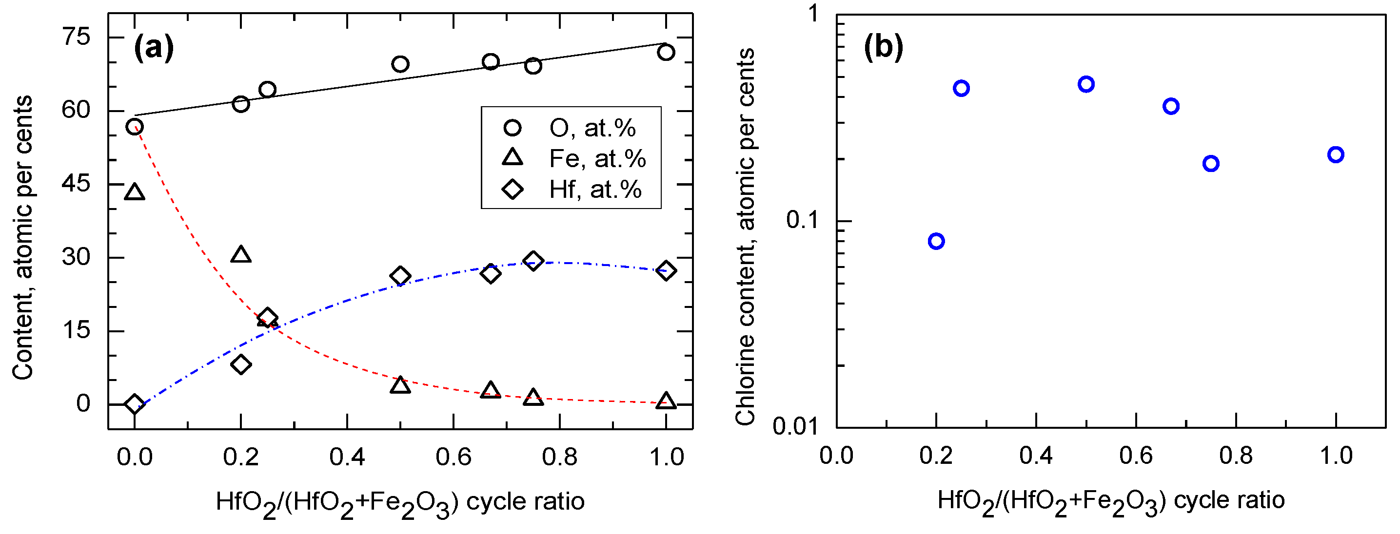
Figure 1. Contents of elements (a) and residual impurities (b) measured by XRF, constituting the HfO2-Fe2O3 films, expressed in atomic% against relative amount of HfO2 deposition cycles. The elements are indicated in the legends. Polynomial lines are guides for the eye.
Nanomaterials 12 02593 g001
Figure 2. X-ray reflectivity results for selected stacks of Fe2O3 and HfO2 layers grown on Si, denoted by the labels revealing the amounts of ALD cycles used for the deposition of constituent layers. The thicknesses of constituent layers as the results of the curve fittings are also given by labels. The curves with fitting results are presented for the four-layer laminate grown using equal amounts of cycles for both constituent oxides (a), the three-layer laminate grown using equal amounts of cycles for both constituent oxides (b), the double-layer consisting of relatively thicker Fe2O3 and thinner HfO2 films (c), and the four-layer laminate containing Fe2O3 layers relatively thicker compared to the HfO2 component (d).
Nanomaterials 12 02593 g002
Figure 3. Bright field STEM images of HfO2-Fe2O3-HfO2 nanolaminate grown using 100 ALD cycles for each constituent layer, taken under different magnifications (a,b), and an image of the interface between silicon substrate and the first HfO2 layer in the same laminate (c).
Nanomaterials 12 02593 g003
Figure 4. Elemental mapping for iron (a), hafnium (b), and oxygen (c) in the HfO2-Fe2O3-HfO2 nanolaminate grown using 100 ALD cycles for each constituent layer.
Nanomaterials 12 02593 g004
Figure 5. Grazing incidence X-ray diffraction patterns of Fe2O3-, HfO2-, and HfO2-Fe2O3-laminated films. The growth cycle sequences are denoted by labels. The reflections supplied with Miller indexes are assigned as those belonging to either monoclinic (M, ICDD PDF-2 card no 43-1017) or tetragonal (T, card 01-078-5756) HfO2, whereby reflections from rhombohedral hematite Fe2O3 are denoted by R (card 01-1053).
Nanomaterials 12 02593 g005
Figure 6. Magnetization-field curves from reference HfO2 and Fe2O3 films measured at 5 K (a) and at 300 K (b), as compared to the curves from HfO-Fe2O3-laminated structures measured at 5 K (c) and 300 K (d). The films were grown on SiO2/Si substrates using cycle sequences represented by labels.
Nanomaterials 12 02593 g006
Figure 7. Magnetic moment (a) and coercivity (b) against relative content of hafnium, expressed by Hf/(Hf + Fe) cation ratio, in HfO2-Fe2O3 nanolaminates. For the cycle ratios and sequences applied for the growth of the samples with the corresponding atomic ratios, see Table 1.
Nanomaterials 12 02593 g007
Figure 8. Magnetization-temperature curves measured in zero-field-cooling (ZFC) and field-cooling (FC) mode from representative structures consisting of two HfO2-Fe2O3 double layers (a) and one HfO2-Fe2O3-HfO2 triple layer (b). The films were grown on diamagnetic SiO2/Si substrates using cycle sequences represented by labels.
Nanomaterials 12 02593 g008
Figure 9. Permittivity versus measurement frequency dispersion test results for reference HfO2 films as well as nanolaminate stacks grown using amounts of ALD cycles and to the thicknesses indicated by the labels. The capacitor electrode areas were 0.002 mm2.
Nanomaterials 12 02593 g009
Figure 10. Current-voltage characteristics demonstrating unipolar switching in TiN/HfO2/Ti devices containing HfO2 films grown to thicknesses of 24 (a) and 54 nm (b) using 200 and 500 ALD cycles, respectively.
Nanomaterials 12 02593 g010
Figure 11. Current-voltage characteristics demonstrating unipolar switching in TiN/HfO2-Fe2O3/Ti devices containing (a) periodically laminated media grown using relatively large amounts of HfO2 deposition cycles, (b) periodically laminated media grown using the same cycle numbers for HfO2 and Fe2O3, and (c) three-layer stack with Fe2O3 layer grown in between HfO2 films. The deposition cycle sequences are indicated by labels.
Nanomaterials 12 02593 g011
Figure 12. Current values measured after each RESET (HRS points) and SET (LRS points) processes at 0.1 V in TiN/HfO2-Fe2O3/Ti devices containing (a) 500 and (b) 200 ALD cycles of HfO2, (c) three-layer stack with Fe2O3 layer grown in between HfO2 films, and (d) periodically laminated media grown using the same cycle numbers for HfO2 and Fe2O3. The deposition cycle sequences are indicated by labels.
Nanomaterials 12 02593 g012
Table 1. List of HfO2, Fe2O3, and HfO2-Fe2O3 samples revealing the deposition cycle sequences, relative HfO2/(HfO2 + Fe2O3) deposition cycle ratio, total film thickness in accord with XRR, and relative Hf/(Hf + Fe) cation ratio measured by XRF and EDS. The samples are presented in the order of decreasing relative cycle ratio for HfO2 and, concurrently, descending cation ratio for Hf, measured by XRF. For the contents of residual chlorine, also measured by XRF, see Figure 1.
Cycle SequenceCycle Ratiottotal, nmHf/(Hf + Fe) by XRF Hf/(Hf + Fe) by EDS
500 × HfO215411
2 × (150 × HfO2 +50 × Fe2O3)0.75230.96 (0.03)0.98
100 × HfO2 + 100 × Fe2O3 + 100 × HfO20.67270.91 (0.04)0.95
2 × (100 × HfO2 +100 × Fe2O3)0.5260.88 (0.02)0.91
2 × (50 × HfO2 +150 × Fe2O3)0.25290.51 (0.01)0.49
400 × Fe2O3 +100 × HfO20.2630.21 (0.01)0.24
500 × Fe2O303700
Publisher’s Note: MDPI stays neutral with regard to jurisdictional claims in published maps and institutional affiliations.

