
Tailoring of AlAs/InAs/GaAs QDs Nanostructures via Capping Growth Rate

 , , ,
, , ,
Abstract
:
1. Introduction
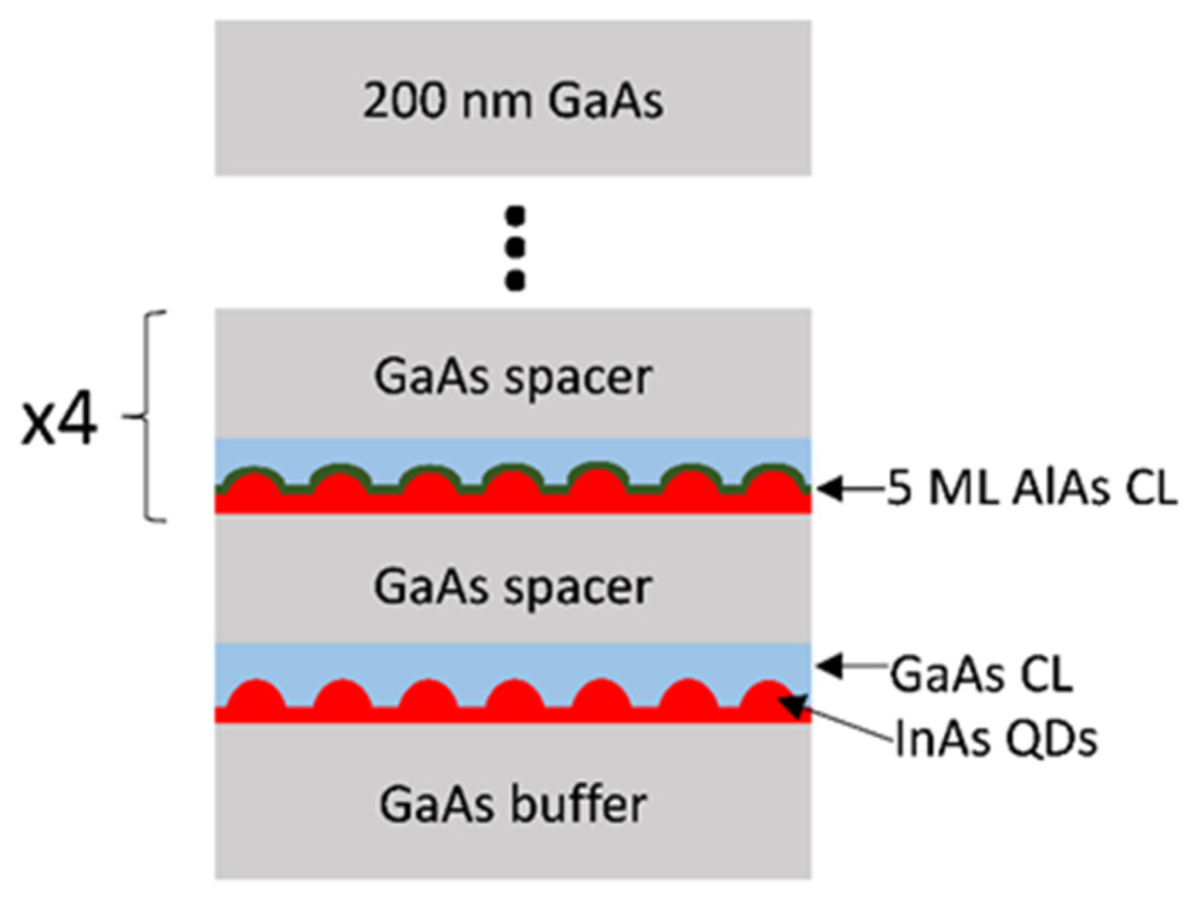
2. Materials and Methods
3. Results
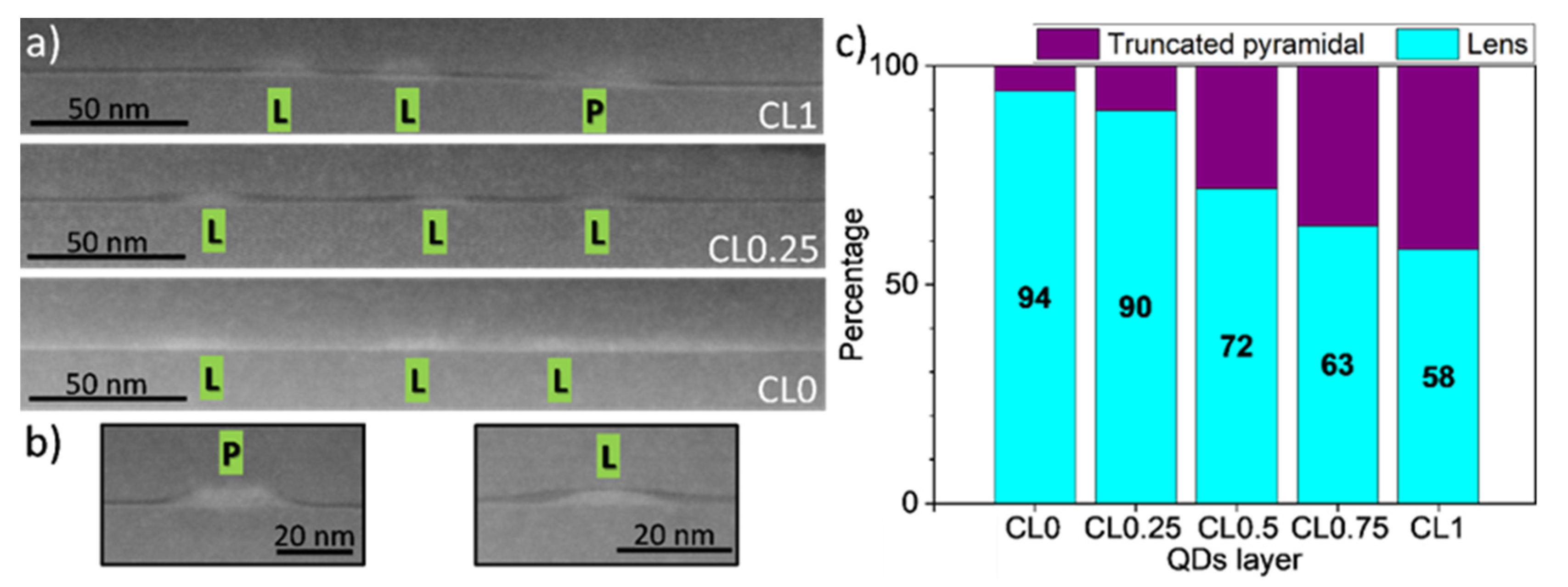
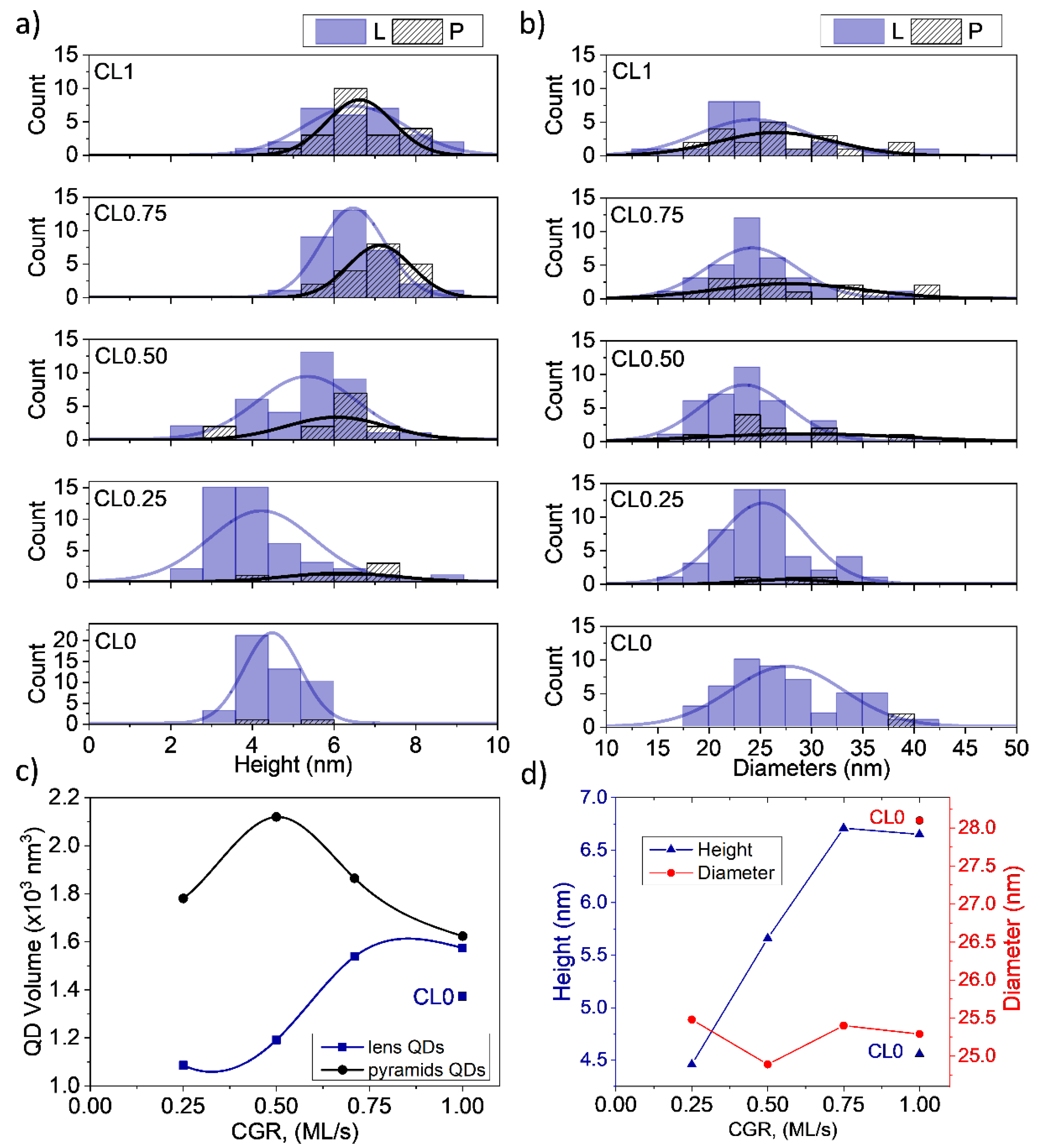
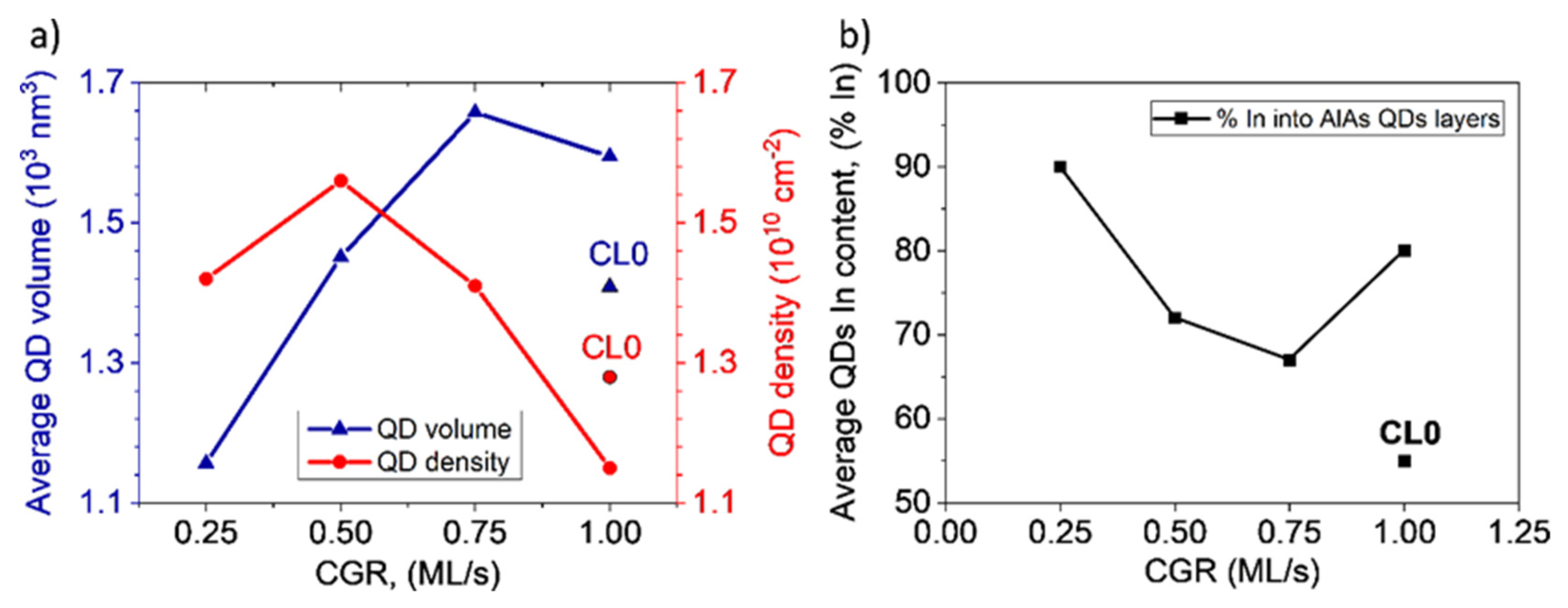
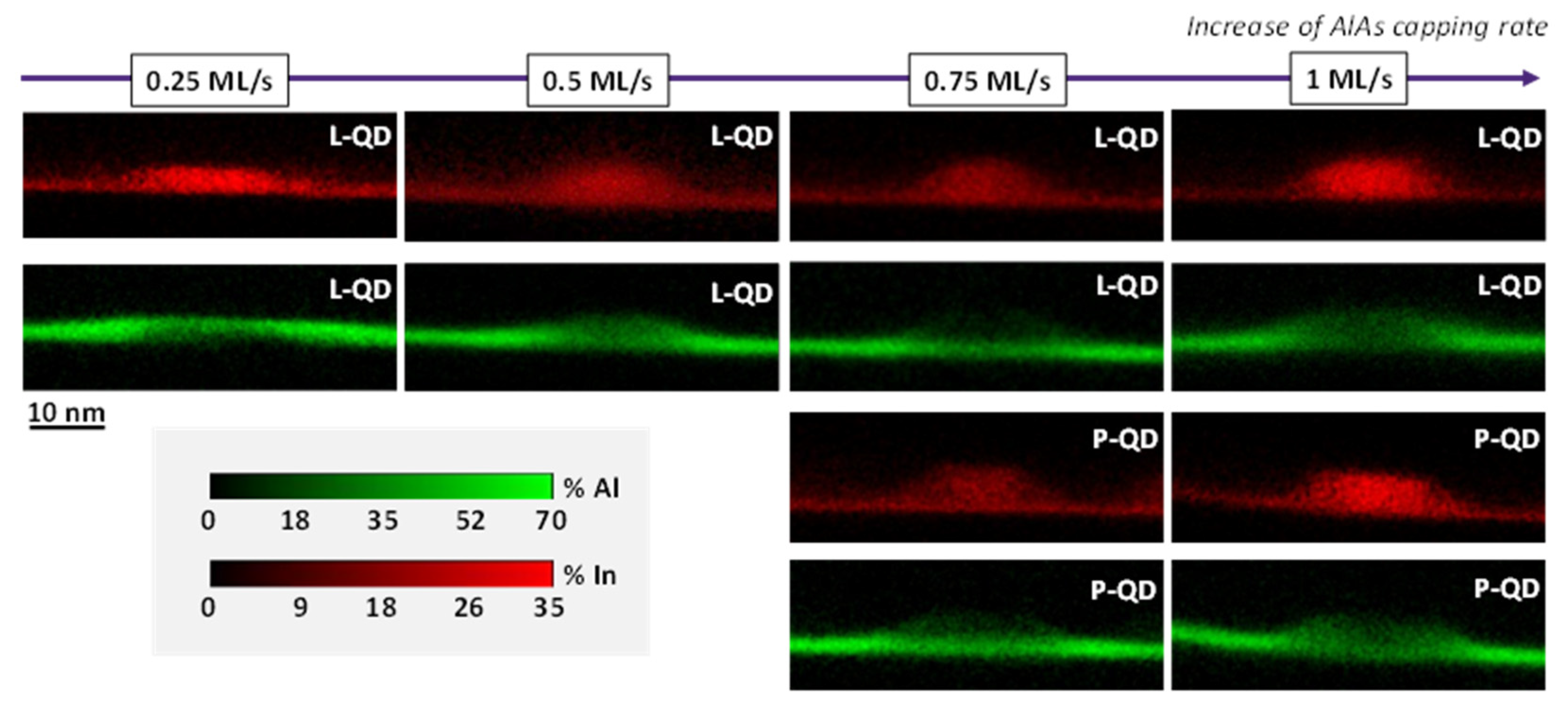
3.1. Structural Analysis of InAs QDs
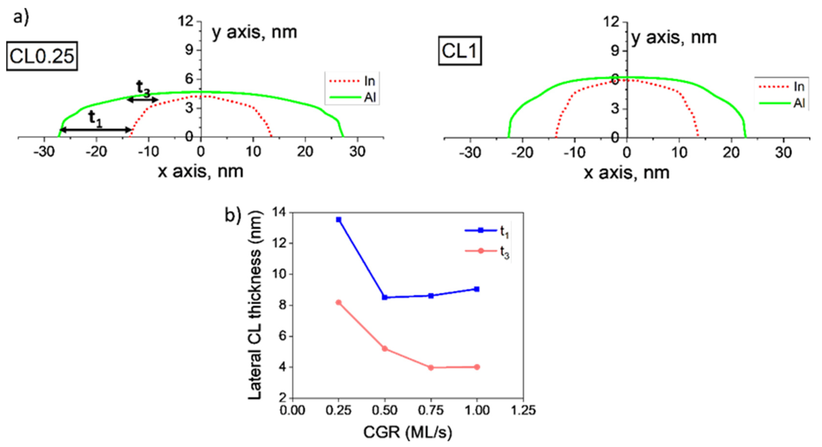
3.2. Analysis of AlAs CL around the QD
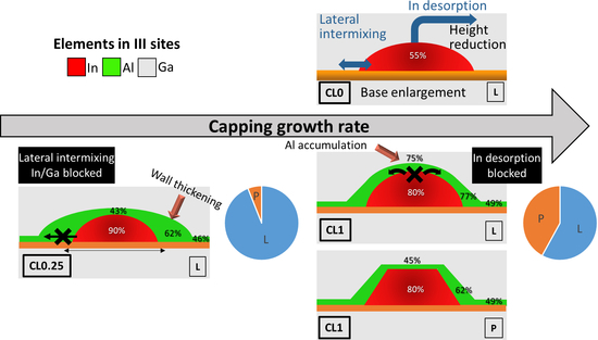
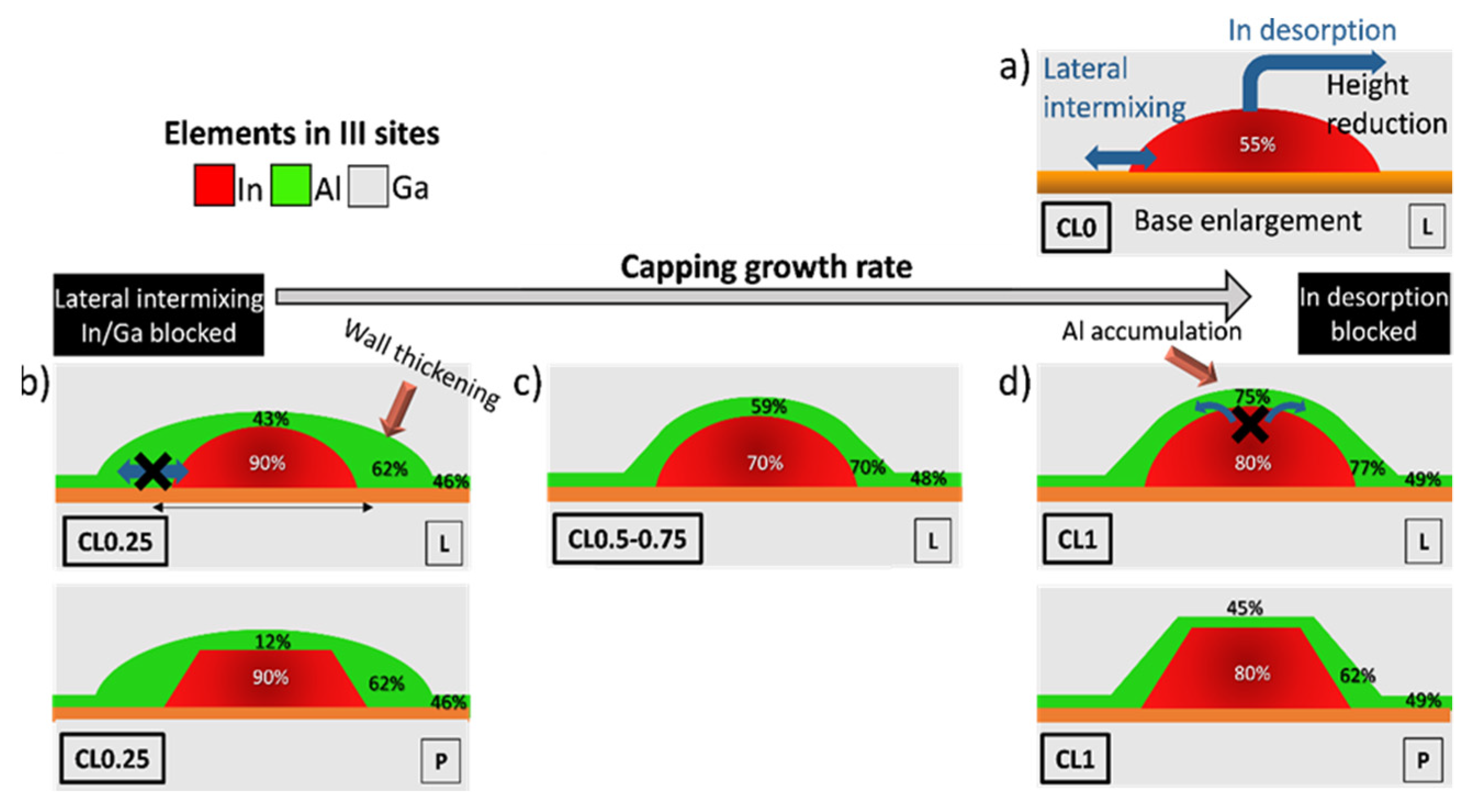
4. Discussion
5. Conclusions
Author Contributions
Funding
Institutional Review Board Statement
Informed Consent Statement
Data Availability Statement
Acknowledgments
Conflicts of Interest
References
- Popescu, V.; Bester, G.; Hanna, M.C.; Norman, A.G.; Zunger, A. Theoretical and Experimental Examination of the Intermediate-Band Concept for Strain-Balanced (In,Ga)As/Ga(As,P) Quantum Dot Solar Cells. Phys. Rev. B Condens. Matter Mater. Phys. 2008, 78, 205321. [Google Scholar] [CrossRef] [Green Version]
- Watanabe, S.; Asahi, S.; Kada, T.; Hirao, K.; Kaizu, T.; Harada, Y.; Kita, T. Two-Step Photocurrent Generation Enhanced by Miniband Formation in InAs/GaAs Quantum Dot Superlattice Intermediate-Band Solar Cells. Appl. Phys. Lett. 2017, 110, 193104. [Google Scholar] [CrossRef] [Green Version]
- Luque, A.; Martí, A.; Stanley, C.; López, N.; Cuadra, L.; Zhou, D.; Pearson, J.L.; McKee, A. General Equivalent Circuit for Intermediate Band Devices: Potentials, Currents and Electroluminescence. J. Appl. Phys. 2004, 96, 903–909. [Google Scholar] [CrossRef]
- Hubbard, S.M.; Cress, C.D.; Bailey, C.G.; Raffaelle, R.P.; Bailey, S.G.; Wilt, D.M. Effect of Strain Compensation on Quantum Dot Enhanced GaAs Solar Cells. Appl. Phys. Lett. 2008, 92, 123512. [Google Scholar] [CrossRef]
- Okada, Y.; Oshima, R.; Takata, A. Characteristics of InAs/GaNAs Strain-Compensated Quantum Dot Solar Cell. J. Appl. Phys. 2009, 106, 024306. [Google Scholar] [CrossRef]
- Bailey, C.G.; Forbes, D.V.; Polly, S.J.; Bittner, Z.S.; Dai, Y.; MacKos, C.; Raffaelle, R.P.; Hubbard, S.M. Open-Circuit Voltage Improvement of InAs/GaAs Quantum-Dot Solar Cells Using Reduced InAs Coverage. IEEE J. Photovolt. 2012, 2, 269–275. [Google Scholar] [CrossRef]
- Luque, A.; Martí, A. The Intermediate Band Solar Cell: Progress toward the Realization of an Attractive Concept. Adv. Mater. 2010, 22, 160–174. [Google Scholar] [CrossRef] [Green Version]
- Beattie, N.S.; See, P.; Zoppi, G.; Ushasree, P.M.; Duchamp, M.; Farrer, I.; Ritchie, D.A.; Tomić, S. Quantum Engineering of InAs/GaAs Quantum Dot Based Intermediate Band Solar Cells. ACS Photonics 2017, 4, 2745–2750. [Google Scholar] [CrossRef]
- Sellers, D.G.; Polly, S.; Hubbard, S.M.; Doty, M.F. Analyzing Carrier Escape Mechanisms in InAs/GaAs Quantum Dot p-i-n Junction Photovoltaic Cells. Appl. Phys. Lett. 2014, 104, 223903. [Google Scholar] [CrossRef]
- Antolín, E.; Martí, A.; Farmer, C.D.; Linares, P.G.; Hernández, E.; Sánchez, A.M.; Ben, T.; Molina, S.I.; Stanley, C.R.; Luque, A. Reducing Carrier Escape in the InAs/GaAs Quantum Dot Intermediate Band Solar Cell. J. Appl. Phys. 2010, 108, 064513. [Google Scholar] [CrossRef] [Green Version]
- Guimard, D.; Morihara, R.; Bordel, D.; Tanabe, K.; Wakayama, Y.; Nishioka, M.; Arakawa, Y. Fabrication of InAs/GaAs Quantum Dot Solar Cells with Enhanced Photocurrent and without Degradation of Open Circuit Voltage. Appl. Phys. Lett. 2010, 96, 203507. [Google Scholar] [CrossRef]
- Tutu, F.K.; Lam, P.; Wu, J.; Miyashita, N.; Okada, Y.; Lee, K.H.; Ekins-Daukes, N.J.; Wilson, J.; Liu, H. InAs/GaAs Quantum Dot Solar Cell with an AlAs Cap Layer. Appl. Phys. Lett. 2013, 102, 163907. [Google Scholar] [CrossRef]
- Varghese, A.; Yakimov, M.; Tokranov, V.; Mitin, V.; Sablon, K.; Sergeev, A.; Oktyabrsky, S. Complete Voltage Recovery in Quantum Dot Solar Cells Due to Suppression of Electron Capture. Nanoscale 2016, 8, 7248–7256. [Google Scholar] [CrossRef]
- Ruiz, N.; Fernández, D.; Stanojević, L.; Ben, T.; Flores, S.; Braza, V.; Carro, A.G.; Luna, E.; Ulloa, J.M.; González, D. Suppressing the Effect of the Wetting Layer through AlAs Capping in InAs/GaAs QD Structures for Solar Cells Applications. Nanomaterials 2022, 12, 1368. [Google Scholar] [CrossRef]
- Ruiz-Marín, N.; Reyes, D.F.; Stanojević, L.; Ben, T.; Braza, V.; Gallego-Carro, A.; Bárcena-González, G.; Ulloa, J.M.; González, D. Effect of the AlAs Capping Layer Thickness on the Structure of InAs/GaAs QD. Appl. Surf. Sci. 2022, 573, 151572. [Google Scholar] [CrossRef]
- Gong, Z.; Fang, Z.D.; Xu, X.H.; Miao, Z.H.; Niu, Z.C.; Feng, S.L. Role of Different Cap Layers Tuning the Wavelength of Self-Assembled InAs/GaAs Quantum Dots. J. Phys. Condens. Matter 2003, 15, 5383–5388. [Google Scholar] [CrossRef]
- Keizer, J.G.; Ulloa, J.M.; Utrilla, A.D.; Koenraad, P.M. InAs Quantum Dot Morphology after Capping with In, N, Sb Alloyed Thin Films. Appl. Phys. Lett. 2014, 104, 053116. [Google Scholar] [CrossRef]
- Gonzalez, D.; Reyes, D.F.; Ben, T.; Utrilla, A.D.; Guzman, A.; Hierro, A.; Ulloa, J.M. Influence of Sb/N Contents during the Capping Process on the Morphology of InAs/GaAs Quantum Dots. Sol. Energy Mater. Sol. Cells 2016, 145, 154–161. [Google Scholar] [CrossRef]
- Hospodková, A.; Pangrác, J.; Oswald, J.; Hulicius, E.; Kuldová, K.; Vyskočil, J.; Melichar, K.; Šimeček, T. Influence of Capping Layer on the Properties of MOVPE-Grown InAs/GaAs Quantum Dots. J. Cryst. Growth 2008, 310, 5081–5084. [Google Scholar] [CrossRef]
- Costantini, G.; Rastelli, A.; Manzano, C.; Acosta-Diaz, P.; Songmuang, R.; Katsaros, G.; Schmidt, O.G.; Kern, K. Interplay between Thermodynamics and Kinetics in the Capping of InAs/GaAs(001) Quantum Dots. Phys. Rev. Lett. 2006, 96, 226106. [Google Scholar] [CrossRef] [Green Version]
- González, D.; Flores, S.; Ruiz-marín, N.; Reyes, D.F.; Stanojević, L.; Utrilla, A.D.; Gonzalo, A.; Carro, A.G.; Ulloa, J.M.; Ben, T. Evaluation of Different Capping Strategies in the InAs/GaAs QD System: Composition, Size and QD Density Features. Appl. Surf. Sci. 2021, 537, 148062. [Google Scholar] [CrossRef]
- Utrilla, A.D.; Grossi, D.F.; Reyes, D.F.; Gonzalo, A.; Braza, V.; Ben, T.; González, D.; Guzman, A.; Hierro, A.; Koenraad, P.M.; et al. Size and Shape Tunability of Self-Assembled InAs/GaAs Nanostructures through the Capping Rate. Appl. Surf. Sci. 2018, 444, 260–266. [Google Scholar] [CrossRef]
- Ulloa, J.M.; Reyes, D.F.; Utrilla, A.D.; Guzman, A.; Hierro, A.; Ben, T.; González, D. Capping Layer Growth Rate and the Optical and Structural Properties of GaAsSbN-Capped InAs/GaAs Quantum Dots. J. Appl. Phys. 2014, 116, 134301. [Google Scholar] [CrossRef]
- Hospodková, A.; Pangrác, J.; Vyskočil, J.; Oswald, J.; Vetushka, A.; Caha, O.; Hazdra, P.; Kuldová, K.; Hulicius, E. InAs/GaAs Quantum Dot Capping in Kinetically Limited MOVPE Growth Regime. J. Cryst. Growth 2011, 317, 39–42. [Google Scholar] [CrossRef]
- Heinrichsdorff, F.; Grundmann, M.; Stier, O.; Krost, A.; Bimberg, D. Influence of In/Ga Intermixing on the Optical Properties of InGaAs/GaAs Quantum Dots. J. Cryst. Growth 1998, 195, 540–545. [Google Scholar] [CrossRef]
- Vandewalle, P.; Süsstrunk, S.; Vetterll, M. A Frequency Domain Approach to Registration of Aliased Images with Application to Super-Resolution. EURASIP J. Appl. Signal Process. 2006, 2006, 1–14. [Google Scholar] [CrossRef] [Green Version]
- Cerva, H. Transmission Electron Microscopy of Heteroepitaxial Layer Structures. Appl. Surf. Sci. 1991, 50, 19–27. [Google Scholar] [CrossRef]
- Beanland, R. Dark Field Transmission Electron Microscope Images of III-V Quantum Dot Structures. Ultramicroscopy 2005, 102, 115–125. [Google Scholar] [CrossRef]
- Grieb, T.; Müller, K.; Fritz, R.; Schowalter, M.; Neugebohrn, N.; Knaub, N.; Volz, K.; Rosenauer, A. Determination of the Chemical Composition of GaNAs Using STEM HAADF Imaging and STEM Strain State Analysis. Ultramicroscopy 2012, 117, 15–23. [Google Scholar] [CrossRef]
- Kirmse, H.; Otto, R.; Häusler, I.; Hähnert, I.; Neumann, W. Structural and Analytical Characterisation Pf Semiconductor Quantum Dots by TEM. In Proceedings of the 2nd CEPHONA Workshop on Microscopic Characterisation of Materials and Structures for Photonics, Warsaw, Poland, 22–23 November 2004; pp. 1–16. [Google Scholar]
- McCaffrey, J.P.; Robertson, M.D.; Fafard, S.; Wasilewski, Z.R.; Griswold, E.M.; Madsen, L.D. Determination of the Size, Shape, and Composition of Indium-Flushed Self-Assembled Quantum Dots by Transmission Electron Microscopy. J. Appl. Phys. 2000, 88, 2272–2277. [Google Scholar] [CrossRef]
- Schliwa, A.; Winkelnkemper, M.; Bimberg, D. Impact of Size, Shape, and Composition on Piezoelectric Effects and Electronic Properties of In (Ga) AsGaAs Quantum Dots. Phys. Rev. B Condens. Matter Mater. Phys. 2007, 76, 205324. [Google Scholar] [CrossRef] [Green Version]
- González, D.; Reyes, D.F.; Utrilla, A.D.; Ben, T.; Braza, V.; Guzman, A.; Hierro, A.; Ulloa, J.M. General Route for the Decomposition of InAs Quantum Dots during the Capping Process. Nanotechnology 2016, 27, 125703. [Google Scholar] [CrossRef] [PubMed]
- Blokland, J.H.; Bozkurt, M.; Ulloa, J.M.; Reuter, D.; Wieck, A.D.; Koenraad, P.M.; Christianen, P.C.M.; Maan, J.C. Ellipsoidal InAs Quantum Dots Observed by Cross-Sectional Scanning Tunneling Microscopy. Appl. Phys. Lett. 2009, 94, 023107. [Google Scholar] [CrossRef] [Green Version]
- Hasan, S.; Merckling, C.; Pantouvaki, M.; Meersschaut, J.; Van Campenhout, J.; Vandervorst, W. Thermodynamic Modelling of InAs/InP(0 0 1) Growth towards Quantum Dots Formation by Metalorganic Vapor Phase Epitaxy. J. Cryst. Growth 2019, 509, 133–140. [Google Scholar] [CrossRef]
- Zhang, H.R.; Egerton, R.F.; Malac, M. Local Thickness Measurement through Scattering Contrast and Electron Energy-Loss Spectroscopy. Micron 2012, 43, 8–15. [Google Scholar] [CrossRef]
- Malis, T.; Cheng, S.C.; Egerton, R.F. EELS Log-ratio Technique for Specimen-thickness Measurement in the TEM. J. Electron Microsc. Technol. 1988, 8, 193–200. [Google Scholar] [CrossRef]
- Ferdos, F.; Wang, S.; Wei, Y.; Larsson, A.; Sadeghi, M.; Zhao, Q. Influence of a Thin GaAs Cap Layer on Structural and Optical Properties of InAs Quantum Dots. Appl. Phys. Lett. 2002, 81, 1195–1197. [Google Scholar] [CrossRef]
- Joyce, P.; Krzyzewski, T.; Bell, G.; Joyce, B. Composition of InAs Quantum Dots on GaAs(001): Direct Evidence for (In, Ga)As Alloying. Phys. Rev. B Condens. Matter Mater. Phys. 1998, 58, R15981–R15984. [Google Scholar] [CrossRef]
- González, D.; Braza, V.; Utrilla, A.D.; Gonzalo, A.; Reyes, D.F.; Ben, T.; Guzman, A.; Hierro, A.; Ulloa, J.M. Quantitative Analysis of the Interplay between InAs Quantum Dots and Wetting Layer during the GaAs Capping Process. Nanotechnology 2017, 28, 425702. [Google Scholar] [CrossRef]
- Kratzer, P.; Liu, Q.K.K.; Acosta-Diaz, P.; Manzano, C.; Costantini, G.; Songmuang, R.; Rastelli, A.; Schmidt, O.G.; Kern, K. Shape Transition during Epitaxial Growth of InAs Quantum Dots on GaAs(001): Theory and Experiment. Phys. Rev. B 2006, 73, 205347. [Google Scholar] [CrossRef] [Green Version]
- Eisele, H.; Lenz, A.; Heitz, R.; Timm, R.; Dähne, M.; Temko, Y.; Suzuki, T.; Jacobi, K. Change of InAs/GaAs Quantum Dot Shape and Composition during Capping. J. Appl. Phys. 2008, 104, 124301. [Google Scholar] [CrossRef]
- Kasu, M.; Kobayashi, N. Surface Diffusion of AlAs on GaAs in Metalorganic Vapor Phase Epitaxy Studied by High-Vacuum Scanning Tunneling Microscopy. Appl. Phys. Lett. 1995, 67, 2842. [Google Scholar] [CrossRef]
- Kasu, M.; Kobayashi, N. Surface-Diffusion and Step-Bunching Mechanisms of Metalorganic Vapor-Phase Epitaxy Studied by High-Vacuum Scanning Tunneling Microscopy. J. Appl. Phys. 1995, 78, 3026–3035. [Google Scholar] [CrossRef]
- Fujiwara, K.; Ishii, A.; Aisaka, T. First Principles Calculation of Indium Migration Barrier Energy on an InAs(001) Surface. Thin Solid Films 2004, 464, 35–37. [Google Scholar] [CrossRef]
- Ferdos, F.; Wang, S.; Wei, Y.; Sadeghi, M.; Zhao, Q.; Larsson, A. Influence of Initial GaAs and AlAs Cap Layers on InAs Quantum Dots Grown by Molecular Beam Epitaxy. J. Cryst. Growth 2003, 251, 145–149. [Google Scholar] [CrossRef]
- Arzberger, M.; Käsberger, U.; Böhm, G.; Abstreiter, G. Influence of a Thin AlAs Cap Layer on Optical Properties of Self-Assembled InAs/GaAs Quantum Dots. Appl. Phys. Lett. 1999, 75, 3968–3970. [Google Scholar] [CrossRef]


Publisher’s Note: MDPI stays neutral with regard to jurisdictional claims in published maps and institutional affiliations. |
© 2022 by the authors. Licensee MDPI, Basel, Switzerland. This article is an open access article distributed under the terms and conditions of the Creative Commons Attribution (CC BY) license (https://creativecommons.org/licenses/by/4.0/).
Share and Cite
Ruiz, N.; Fernandez, D.; Luna, E.; Stanojević, L.; Ben, T.; Flores, S.; Braza, V.; Gallego-Carro, A.; Bárcena-González, G.; Yañez, A.; et al. Tailoring of AlAs/InAs/GaAs QDs Nanostructures via Capping Growth Rate. Nanomaterials 2022, 12, 2504. https://doi.org/10.3390/nano12142504
Ruiz N, Fernandez D, Luna E, Stanojević L, Ben T, Flores S, Braza V, Gallego-Carro A, Bárcena-González G, Yañez A, et al. Tailoring of AlAs/InAs/GaAs QDs Nanostructures via Capping Growth Rate. Nanomaterials. 2022; 12(14):2504. https://doi.org/10.3390/nano12142504
Chicago/Turabian StyleRuiz, Nazaret, Daniel Fernandez, Esperanza Luna, Lazar Stanojević, Teresa Ben, Sara Flores, Verónica Braza, Alejandro Gallego-Carro, Guillermo Bárcena-González, Andres Yañez, and et al. 2022. "Tailoring of AlAs/InAs/GaAs QDs Nanostructures via Capping Growth Rate" Nanomaterials 12, no. 14: 2504. https://doi.org/10.3390/nano12142504
APA StyleRuiz, N., Fernandez, D., Luna, E., Stanojević, L., Ben, T., Flores, S., Braza, V., Gallego-Carro, A., Bárcena-González, G., Yañez, A., Ulloa, J. M., & González, D. (2022). Tailoring of AlAs/InAs/GaAs QDs Nanostructures via Capping Growth Rate. Nanomaterials, 12(14), 2504. https://doi.org/10.3390/nano12142504