
Solid Phase Epitaxy of Single Phase Two-Dimensional Layered InSe Grown by MBE

 , , ,
, , , 
Abstract
:1. Introduction
2. Materials and Methods
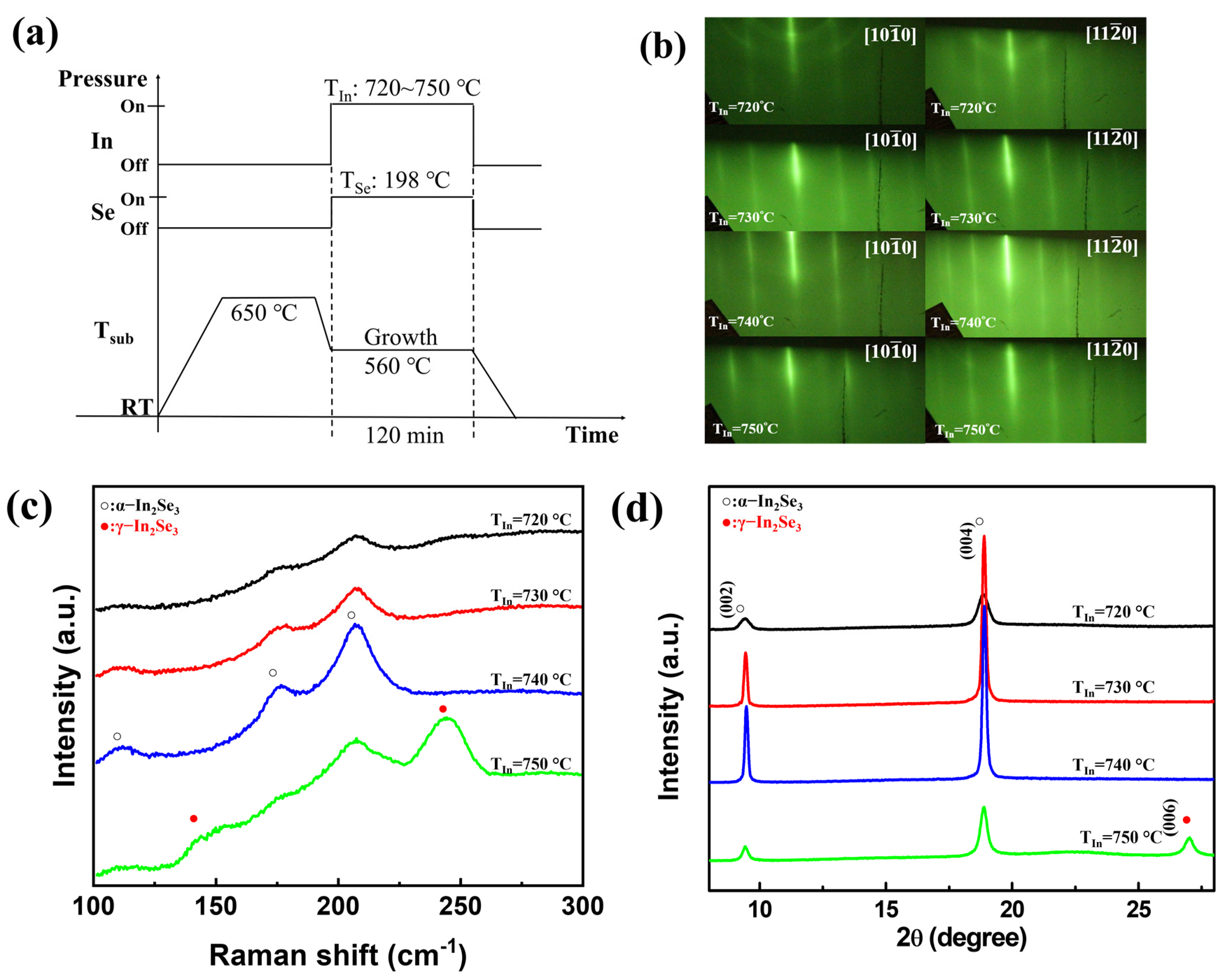
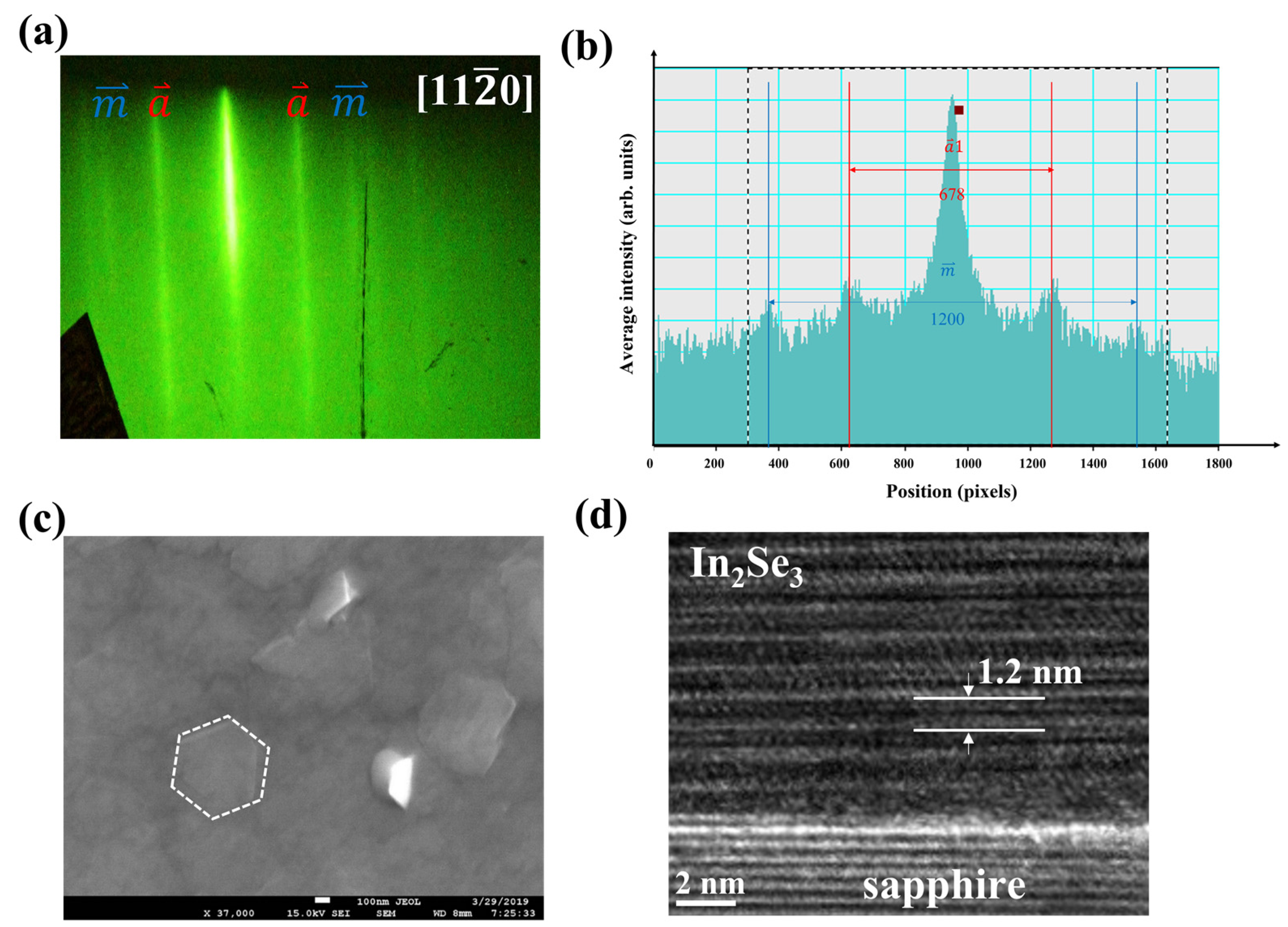
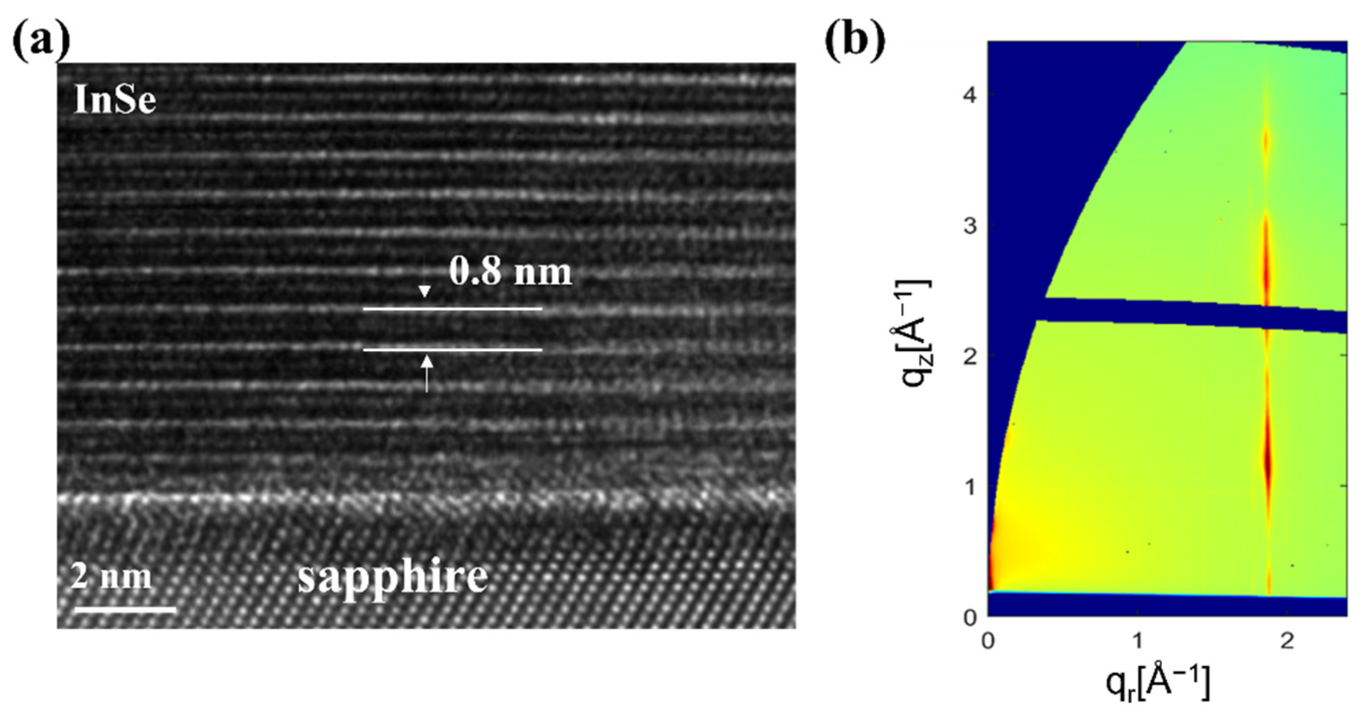
3. Results and Discussion
4. Conclusions
Author Contributions
Funding
Institutional Review Board Statement
Informed Consent Statement
Data Availability Statement
Acknowledgments
Conflicts of Interest
Appendix A

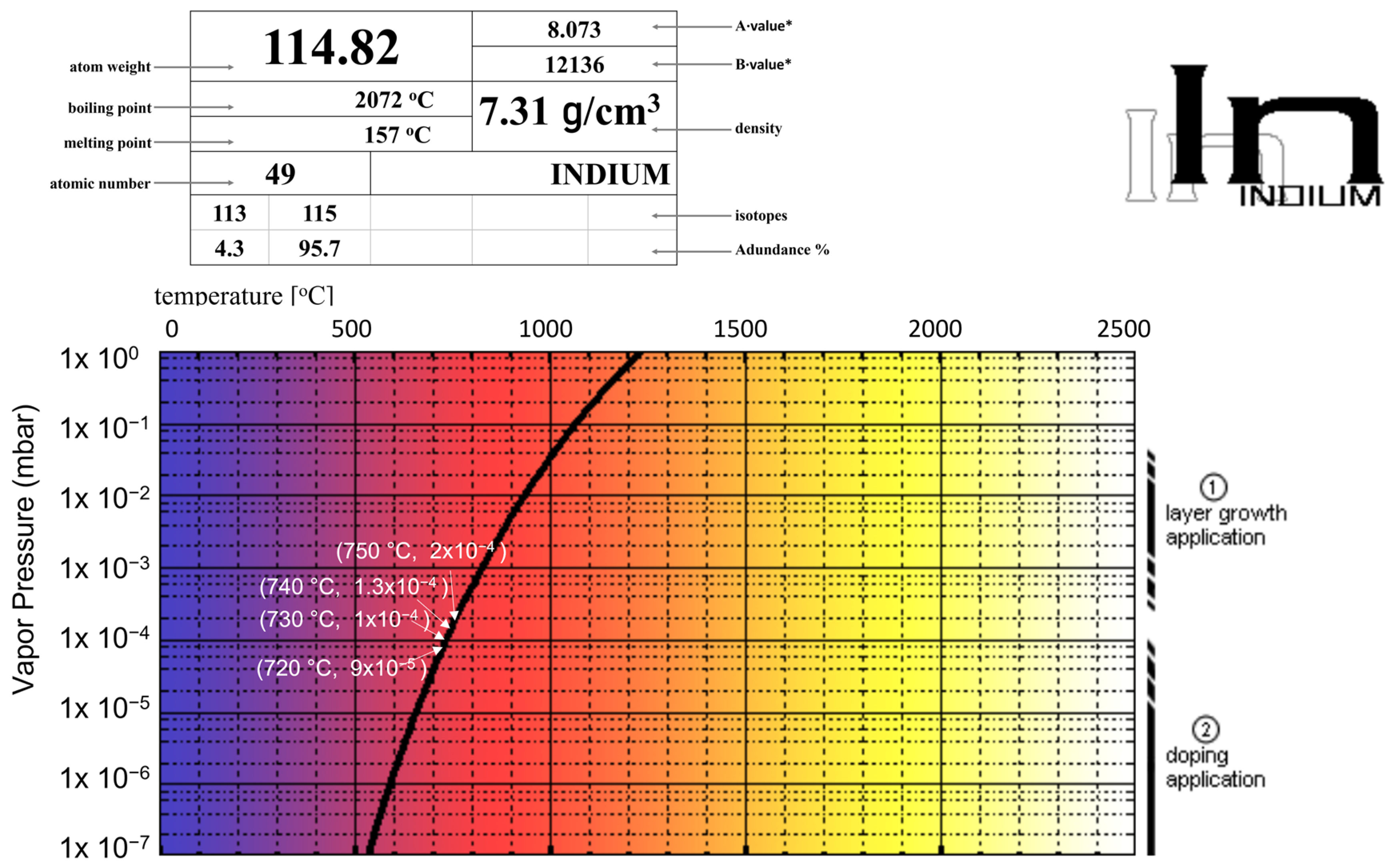
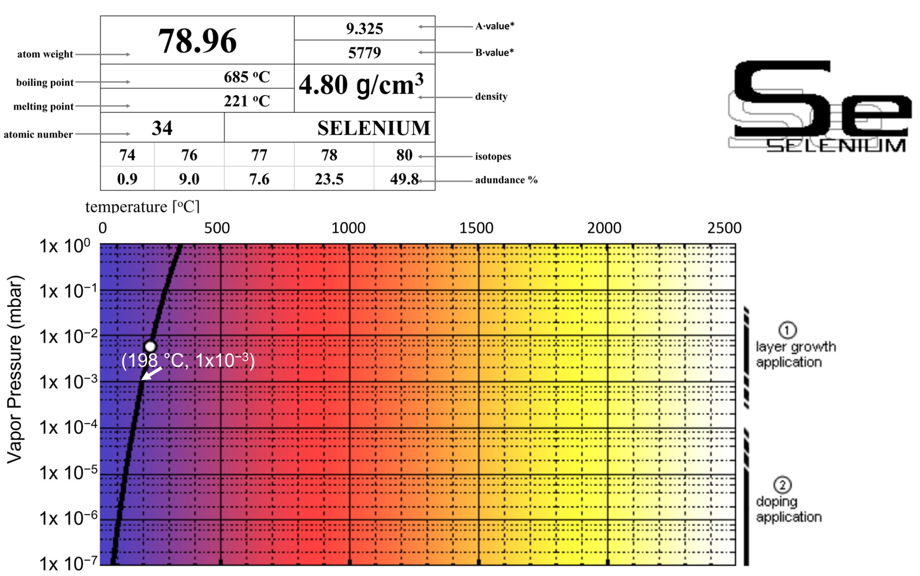
| Material | Mole Mass M | Temperature (°C) | Vapor Pressure (mbar) | Temperature (K) | Za = p/(M*T(K))0.5 | Ratio = Za(In)/Za(Se) |
|---|---|---|---|---|---|---|
| Se | 79 | 198 | 1.00 × 10⁻³ | 471 | 5.18413 × 10⁻⁶ | |
| In | 115 | 720 | 9.00 × 10⁻⁵ | 993 | 2.66329 × 10⁻⁷ | 0.051373951 |
| In | 115 | 730 | 1.00 × 10⁻⁴ | 1003 | 2.94443 × 10⁻⁷ | 0.056796897 |
| In | 115 | 740 | 1.30 × 10⁻⁴ | 1013 | 3.80881 × 10⁻⁷ | 0.073470621 |
| In | 115 | 750 | 2.00 × 10⁻⁴ | 1023 | 5.831 × 10⁻⁷ | 0.112477915 |
References
- Wang, Q.H.; Kalantar-Zadeh, K.; Kis, A.; Coleman, J.N.; Strano, M.S. Electronics and Optoelectronics of Two-Dimensional Transition Metal Dichalcogenides. Nat. Nanotechnol. 2012, 7, 699–712. [Google Scholar] [CrossRef] [PubMed]
- Mak, K.F.; Shan, J. Photonics and optoelectronics of 2D semiconductor transition metal dichalcogenides. Nat. Photonics 2016, 10, 216–226. [Google Scholar] [CrossRef]
- Sánchez-Royo, J.F.; Muñoz-Matutano, G.; Brotons-Gisbert, M.; Martínez-Pastor, J.P.; Segura, A.; Cantarero, A.; Mata, R.; Canet-Ferrer, J.; Tobias, G.; Canadell, E.; et al. Electronic structure, optical properties, and lattice dynamics in atomically thin indium selenide flakes. Nano Res. 2014, 7, 1556–1568. [Google Scholar] [CrossRef]
- Feng, W.; Zheng, W.; Cao, W.; Hu, P. Back Gated Multilayer InSe Transistors with Enhanced Carrier Mobilities via the Suppression of Carrier Scattering from a Dielectric Interface. Adv. Mater. 2014, 26, 6587–6593. [Google Scholar] [CrossRef] [PubMed]
- Sucharitakul, S.; Goble, N.J.; Kumar, U.R.; Sankar, R.; Bogorad, Z.A.; Chou, F.; Chen, Y.; Gao, X.P.A. Intrinsic Electron Mobility Exceeding 10³ cm²/(V s) in Multilayer InSe FETs. Nano Lett. 2015, 15, 3815–3819. [Google Scholar] [CrossRef] [Green Version]
- Tamalampudi, S.R.; Lu, Y.-Y.; U, R.K.; Sankar, R.; Liao, C.-D.; Boopathi, K.M.; Cheng, C.-H.; Chou, F.C.; Chen, Y.-T. High Performance and Bendable Few-Layered InSe Photodetectors with Broad Spectral Response. Nano Lett. 2014, 14, 2800–2806. [Google Scholar] [CrossRef]
- Lei, S.; Ge, L.; Najmaei, S.; George, A.; Kappera, R.; Lou, J.; Chhowalla, M.; Yamaguchi, H.; Gupta, G.; Vajtai, R.; et al. Evolution of the electronic band structure and efficient photo-detection in atomic layers of InSe. ACS Nano 2014, 8, 1263–1272. [Google Scholar] [CrossRef]
- Lei, S.; Wen, F.; Li, B.; Wang, Q.; Huang, Y.; Gong, Y.; He, Y.; Dong, P.; Bellah, J.; George, A.; et al. Optoelectronic Memory Using Two-Dimensional Materials. Nano Lett. 2015, 15, 259–265. [Google Scholar] [CrossRef]
- Cantrell, D.A. High electron mobility, quantum Hall effect and anomalous optical response in atomically thin InSe. Nat. Nanotechnol. 2017, 12, 223–227. [Google Scholar]
- Zhang, X.; Lee, S.; Bansal, A.; Zhang, F.; Terrones, M.; Jackson, T.N.; Redwing, J.M. Epitaxial growth of few-layer β-In2Se3 thin films by metalorganic chemical vapor deposition. J. Cryst. Growth 2020, 533, 125471. [Google Scholar] [CrossRef]
- Küpers, M.; Konze, P.M.; Meledin, A.; Mayer, J.; Englert, U.; Wuttig, M.; Dronskowski, R. Controlled Crystal Growth of Indium Selenide, In2Se3, and the Crystal Structures of α-In2Se3. Inorg. Chem. 2018, 57, 11775–11781. [Google Scholar] [CrossRef] [PubMed] [Green Version]
- Huang, W.; Gan, L.; Li, H.; Ma, Y.; Zhai, T. Phase-Engineered Growth of Ultrathin InSe Flakes by Chemical Vapor Deposition for High-Efficiency Second Harmonic Generation. Chem. Eur. J. 2018, 24, 15678–15684. [Google Scholar] [CrossRef] [PubMed]
- Zheng, D.; Shiogai, J.; Fujiwara, K.; Tsukazaki, A. Pulsed-laser deposition of InSe thin films for the detection of thickness-dependent bandgap modification. Appl. Phys. Lett. 2018, 113, 253501. [Google Scholar] [CrossRef]
- Yang, Z.; Jie, W.; Mak, C.; Lin, S.; Lin, H.; Yang, X.; Yan, F.; Lau, S.P.; Hao, J. Wafer-Scale Synthesis of High-Quality Semiconducting Two-Dimensional Layered InSe with Broadband Photoresponse. ACS Nano 2017, 11, 4225–4236. [Google Scholar] [CrossRef] [PubMed]
- Hsiao, S.; Yang, C.; Yang, H.; Wu, C.; Wu, S.; Chang, L.; Ho, Y.; Chang, S.; Chou, W. Novel Method for the Growth of Two-Dimensional Layered InSe Thin Films on Amorphous Substrate by Molecular Beam Epitaxy. Front. Mater. 2022, 9, 871003. [Google Scholar] [CrossRef]
- Rashid, R.; Ling, F.C.-C.; Wang, S.-P.; Xiao, K.; Cui, X.; Ki, Q.R.D.-K. IP and OOP ferroelectricity in hexagonal γ-In2Se3 nanoflakes grown by chemical vapor deposition. J. Alloys Compd. 2021, 870, 159344. [Google Scholar] [CrossRef]
- Hu, Y.; Feng, W.; Dai1, M.; Yang, H.; Chen, X.; Liu, G.; Zhang, S.; Hu, P. Temperature-dependent growth of few layer β-InSe and α-In2Se3 single crystals for optoelectronic device. Semicond. Sci. Technol. 2018, 33, 125002. [Google Scholar] [CrossRef]
- Balakrishnan, N.; Steer, E.D.; Smith, E.F.; Kudrynskyi, Z.R.; Kovalyuk, Z.D.; Eaves, L.; Patanè, A.; Beton, P.H. Epitaxial growth of γ-InSe and α, β, and γ-In2Se3 on ε-GaSe. 2D Mater. 2018, 5, 035026. [Google Scholar] [CrossRef] [Green Version]
- Vishwanath, S.; Liu, X.; Rouvimov, S.; Basile, L.; Lu, N.; Azcatl, A.; Magno, K.; Wallace, R.M.; Kim, M.; Idrobo, J.-C.; et al. Controllable growth of layered selenide and telluride heterostructures and superlattices using molecular beam epitaxy. J. Mater. Res. 2016, 31, 900–910. [Google Scholar] [CrossRef] [Green Version]
- Seredyński, B.; Ogorzałek, Z.; Zajkowska, W.; Bożek, R.; Tokarczyk, M.; Suffczyński, J.; Kret, S.; Sadowski, J.; Gryglas-Borysiewicz, M.; Pacuski, W. Molecular Beam Epitaxy of a 2D Material Nearly Lattice Matched to a 3D Substrate: NiTe2 on GaAs. Cryst. Growth Des. 2021, 21, 5773–5779. [Google Scholar] [CrossRef]
- Pacuski, W.; Grzeszczyk, M.; Nogajewski, K.; Bogucki, A.; Oreszczuk, K.; Kucharek, J.; Połczyńska, K.E.; Seredyński, B.; Rodek, A.; Bożek, R.; et al. Narrow Excitonic Lines and Large-Scale Homogeneity of Transition-Metal Dichalcogenide Monolayers Grown by Molecular Beam Epitaxy on Hexagonal Boron Nitride. Nano Lett. 2020, 20, 3058–3066. [Google Scholar] [CrossRef] [PubMed] [Green Version]
- Han, G.; Chen, Z.; Drennan, J.; Zou, J. Indium Selenides: Structural Characteristics, Synthesis and Their Thermoelectric Performances. Small 2014, 10, 2747–2765. [Google Scholar] [CrossRef] [PubMed]
- Segura, A. Layered Indium Selenide under High Pressure: A Review. Crystals 2018, 8, 206. [Google Scholar] [CrossRef] [Green Version]
- Grimaldi, I.; Gerace, T.; Pipita, M.M.; Perrotta, I.D.; Ciuchi, F.; Berger, H.; Papagno, M.; Castriota, M.; Pacilé, D. Structural investigation of InSe layered semiconductors. Solid State Commun. 2020, 311, 113855. [Google Scholar] [CrossRef]
- Waghmare, A.; Sharma, V.; Shinde, P.; Punde, A.; Vairale, P.; Hase, Y.; Pandharkar, S.; Nair, S.; Aher, R.; Doiphode, V.; et al. Preparation and characterization of γ-In2Se3 thin-film photoanodes for photoelectrochemical water splitting. J. Solid State Electrochem. 2022, 26, 219–232. [Google Scholar] [CrossRef]
- Lewandowska, R.; Bacewicz, R.; Filipowicz, J.; Paszkowicz, W. Raman scattering in α-In2Se3 crystals. Mater. Res. Bull. 2001, 36, 2577–2583. [Google Scholar] [CrossRef]
- Sun, Y.; Pang, S.; Zhang, J. Layer Number-Dependent Raman Spectra of γ-InSe. J. Phys. Chem. Lett. 2022, 13, 3691–3697. [Google Scholar] [CrossRef]
- Liang, D.; Wei, T.; Wang, J.; Li, J. Quasi van der Waals epitaxy nitride materials and devices on two dimension materials. Nano Energy 2020, 69, 104463. [Google Scholar] [CrossRef]
- Liu, C.; Huang, H.; Choi, W.; Kim, J.; Jung, K.; Sun, W.; Tansu, N.; Zhou, W.; Kuo, H.; Li, X. Hybrid Integration of n-MoS2/p-GaN Diodes by Quasi-van der Waals Epitaxy. ACS Appl. Electron. Mater. 2020, 2, 419–425. [Google Scholar] [CrossRef]
- Mortelmans, W.; Gendt, S.; Heyns, M.; Merckling, C. Epitaxy of 2D chalcogenides: Aspects and consequences of weak van der Waals coupling. Appl. Mater. Today 2021, 22, 100975. [Google Scholar] [CrossRef]
- Chang, S.; Wang, S.; Huang, Y.; Chih, J.H.; Lai, Y.; Tsai, Y.; Lin, J.; Chien, C.; Tang, Y.; Hu, C. van der Waals epitaxy of 2D h-AlN on TMDs by atomic layer deposition at 250 °C. Appl. Phys. Lett. 2022, 120, 162102. [Google Scholar] [CrossRef]
- Franz, D.; Blanc, N.; Coraux, J.; Renaud, G.; Runte, S.; Gerber, T.; Busse, C.; Michely, T.; Feibelman, P.J.; Hejral, U.; et al. Atomic Structure of Pt nanoclusters supported by graphene/Ir(111) and reversible transformation under CO exposure. Phys. Rev. B 2016, 93, 045426. [Google Scholar] [CrossRef] [Green Version]
- The Open Quantum Materials Database (OQMD). Available online: https://oqmd.org/materials/composition/InSe (accessed on 2 May 2022).
- The Open Quantum Materials Database (OQMD). Available online: https://oqmd.org/materials/composition/In2Se3 (accessed on 2 May 2022).
- Eberl MBE-Komponenten GmbH. Available online: https://www.mbe-komponenten.de/selection-guide/element/in.php (accessed on 2 May 2022).
- Eberl MBE-Komponenten GmbH. Available online: https://www.mbe-komponenten.de/selection-guide/element/se.php (accessed on 2 May 2022).
- Sarangan, A. Physical and Chemical Vapor Deposition. In Nanofabrication, Principles to Laboratory Practice; CRC Press: Boca Raton, FL, USA, 2016. [Google Scholar]


Publisher’s Note: MDPI stays neutral with regard to jurisdictional claims in published maps and institutional affiliations. |
© 2022 by the authors. Licensee MDPI, Basel, Switzerland. This article is an open access article distributed under the terms and conditions of the Creative Commons Attribution (CC BY) license (https://creativecommons.org/licenses/by/4.0/).
Share and Cite
Wu, C.-H.; Huang, Y.-C.; Ho, Y.-T.; Chang, S.-J.; Wu, S.-K.; Huang, C.-H.; Chou, W.-C.; Yang, C.-S. Solid Phase Epitaxy of Single Phase Two-Dimensional Layered InSe Grown by MBE. Nanomaterials 2022, 12, 2435. https://doi.org/10.3390/nano12142435
Wu C-H, Huang Y-C, Ho Y-T, Chang S-J, Wu S-K, Huang C-H, Chou W-C, Yang C-S. Solid Phase Epitaxy of Single Phase Two-Dimensional Layered InSe Grown by MBE. Nanomaterials. 2022; 12(14):2435. https://doi.org/10.3390/nano12142435
Chicago/Turabian StyleWu, Chia-Hsing, Yu-Che Huang, Yen-Teng Ho, Shu-Jui Chang, Ssu-Kuan Wu, Ci-Hao Huang, Wu-Ching Chou, and Chu-Shou Yang. 2022. "Solid Phase Epitaxy of Single Phase Two-Dimensional Layered InSe Grown by MBE" Nanomaterials 12, no. 14: 2435. https://doi.org/10.3390/nano12142435
APA StyleWu, C.-H., Huang, Y.-C., Ho, Y.-T., Chang, S.-J., Wu, S.-K., Huang, C.-H., Chou, W.-C., & Yang, C.-S. (2022). Solid Phase Epitaxy of Single Phase Two-Dimensional Layered InSe Grown by MBE. Nanomaterials, 12(14), 2435. https://doi.org/10.3390/nano12142435