Article

Optimized Thermoelectric Properties of Sulfide Compound Bi2SeS2 by Iodine Doping

Shenzhen Key Laboratory of Advanced Thin Films and Applications, College of Physics and Optoelectronic Engineering, Shenzhen University, Shenzhen 518060, China
*
Author to whom correspondence should be addressed.
Nanomaterials 2022, 12(14), 2434; https://doi.org/10.3390/nano12142434
Submission received: 24 May 2022 / Revised: 2 July 2022 / Accepted: 13 July 2022 / Published: 15 July 2022
(This article belongs to the Special Issue Synthesis and Performance of Nanostructured Metal Sulfides)

Abstract

:
The Te-free compound Bi2SeS2 is considered as a potential thermoelectric material with less environmentally hazardous composition. Herein, the effect of iodine (I) substitution on its thermoelectric transport properties was studied. The electrical conductivity was enhanced due to the increased carrier concentration caused by the carrier provided defect Ise. Thus, an enhanced power factor over 690 μWm−1K−2 was obtained at 300 K by combining a moderate Seebeck coefficient above 150 µV/K due to its large effective mass, which indicated iodine was an effective n-type dopant for Bi2SeS2. Furthermore, a large drop in the lattice thermal conductivity was observed due to the enhanced phonon scattering caused by nanoprecipitates, which resulted in a low total thermal conductivity (<0.95 Wm−1K−1) for all doped samples. Consequently, a maximum ZT value of 0.56 was achieved at 773 K for a Bi2Se1−xIxS2 (x = 1.1%) sample, a nearly threefold improvement compared to the undoped sample.

1. Introduction

Thermoelectric (TE) materials directly convert electrical and thermal energy without emitting harmful substances and are considered environmentally friendly materials with huge development potential and broadly applicability [1,2,3,4]. Generally, the energy conversion efficiencies of TE materials are evaluated by ZT (ZT = σS2T/κ), where σ, S, κ, and T are the electrical conductivity, Seebeck coefficient, thermal conductivity, and the absolute temperature, respectively [5,6,7]. Therefore, an outstanding TE material should have a high ZT with high electrical conductivity, large Seebeck coefficient, and low thermal conductivity. The optimization of these intuitive interdependent parameters poses a significant challenge. However, the design of rational experimental strategies has continuously rewritten the record of ZT over the past twenty years [8,9,10,11,12,13].
As two important conventional TE materials, Bi2Te3 and PbTe are the best and most stable materials used near room temperature and mid-temperature [14,15]; however, large-scale commercial applications in the future are limited due to the extensive use of toxic Pb and Te [16]. Thus, developing Te-free and Pb-free candidates with high TE performance represents a significant and important challenge [17,18]. Recently, environmentally friendly sulfide compounds have received widespread attention. Bi2S3 is a typical example of the sulfide counterpart of Bi2Te3, with a similar crystal structure [19,20]. Despite its poor electrical conductivity and high thermal conductivity that results in a dismally low ZT (0.055), TE properties have been optimized using several effective strategies, which include elemental doping, texturing, and microstructure design [21,22,23,24,25,26]. However, most reported ZT values are < 0.6, relatively low compared to traditional materials [21,22,23,24,25,26]. Poor TE properties for the sulfide compounds stem primarily from low electrical conductivity and high lattice thermal conductivity due to the light atomic weights and either too high or too low carrier concentrations.
Recent reports revealed that the ternary sulfide compound Bi2SeS2 has TE potential with a high ZT (>1.0) [27,28]. Its crystalline structure was similar to Bi2S3. But the Bi2SeS2 band gap of ~1.0 eV was narrower than Bi2S3 (~1.35 eV), which caused reasonably satisfactory electrical conductivity. Combined with low thermal conductivity (<0.8 W m−1K−1), a ZT value of 0.25 was obtained for the pure sample [29]. By tuning the electrical conductivity via Cu doping and suppressing the lattice thermal conductivity by forming nanoprecipitates, the ZT value increased to 0.7 at 723 K, and to 1.0 at 773 K [27,30]. Recently, Br served as an effective carrier donor and induced a partial Bi2SeS2 phase change from Pnma to Pnnm, which formed a quasi homo-composition and a hetero-structure (hoC-heS) nanocomposite [28]. This caused a significant lattice thermal conductivity decrease and enhanced power factor, which resulted in a large ZT value improvement.
Halogens are well-known n-type dopants for the Bi2X3 family (X = Te, Se, and S), with defects in Clx, Brx, or Ix providing free electrons to increase carrier concentrations [31,32]. Aside from Br doping, the effect of single Cl or I doping on TE transport properties of Bi2SeS2 has not been reported. Whether Cl or I would induce the phase transition of Bi2SeS2 merits consideration. Hence, this motivated us to conduct this study. Herein, iodine (I) was chosen as a dopant in the Bi2SeS2 system. Although no phase transition was found after iodine doping, an enhanced power factor due to the increased carrier density, together with a reduced lattice thermal conductivity due to the enhanced phonon scattering, was obtained. A maximal ZT of 0.56 at 773 K was achieved for Bi2Se1−xIxS2 with x = 1.1%, three times higher than the undoped sample, which indicated iodine was an effective n-type dopant for Bi2SeS2.

2. Experimental

A series of Bi2Se1−xIxS2 (x = 0, 0.1%, 0.3%, 0.5%, 0.7%, 0.9%, 1.1%, and 1.3%) ingots were synthesized by a combination of solid-state reaction and spark plasma sintering (SPS) using high-purity powders of Bi (99.99%), Se (99.99%), S (99.95%) and BiI3 (99.99%). Stoichiometric powder mixtures were roughly mixed and placed into glass ampoules according to their compositions. The ampoules were sealed under vacuum (<10−3 Pa) and heated at 1173 K for 12 h with subsequent annealing at 773 K for 48 h. Ingots were obtained upon cooling to 300 K and pulverized into micron-sized powders by hand grinding. The powder was placed into a mold and sintered in as SPS furnace at 773 K for 5 min with an axial pressure of 50 MPa to form column-shaped bulk sample. Two pieces were obtained from one bulk sample. One piece was used to measure the electrical conductivity and Seebeck coefficient along the direction perpendicular to the SPS pressing direction; the other piece was used to test its thermal conductivity in the same direction.
Crystal structures were determined by X-ray diffraction (XRD, Ultima IV, Riguku, Japan) using Cu Kα radiation and a scanning rate of 5°/min. Rietveld refinement was performed using the Generalized Structural Analysis System (GSAS-II) program. The micromorphologies of the fractured surfaces and backscattered electron imaging (BES) on the polished surfaces were detected via field scanning electron microscopy (FSEM, Supra 55 Sapphire, Zeiss, Germany). The energy dispersive spectroscopy (EDS) equipment attached to the FSEM analyzed the elemental compositions and distributions. The electrical resistivity and the Seebeck coefficient were measured from room temperature to 773 K using an electric resistance/Seebeck coefficient measuring system (ZEM-3, Ulvac-Riko, Japan). The Hall coefficients (RH) at room temperature were tested by a Van der Pauw technique. Based on the expression μ = σRH and n = 1/(eRH), where σ is the electrical conductivity, the carrier mobility (μ) and the carrier concentration (n) were calculated. The thermal diffusivity (D) was determined using laser flash diffusivity (Netzsch LFA467, Germany), which was then used to calculate the total thermal conductivity (κ) using κ = DCpρ, where ρ is the bulk density of the sample, and Cp is the heat capacity. Cp values were tested using two differential scanning calorimeters (DSC); a DSC200-F3 yielded Cp values from 298–523 K; a DSC404-C gave Cp values from 523–773 K. Densities were determined by the Archimedes method.

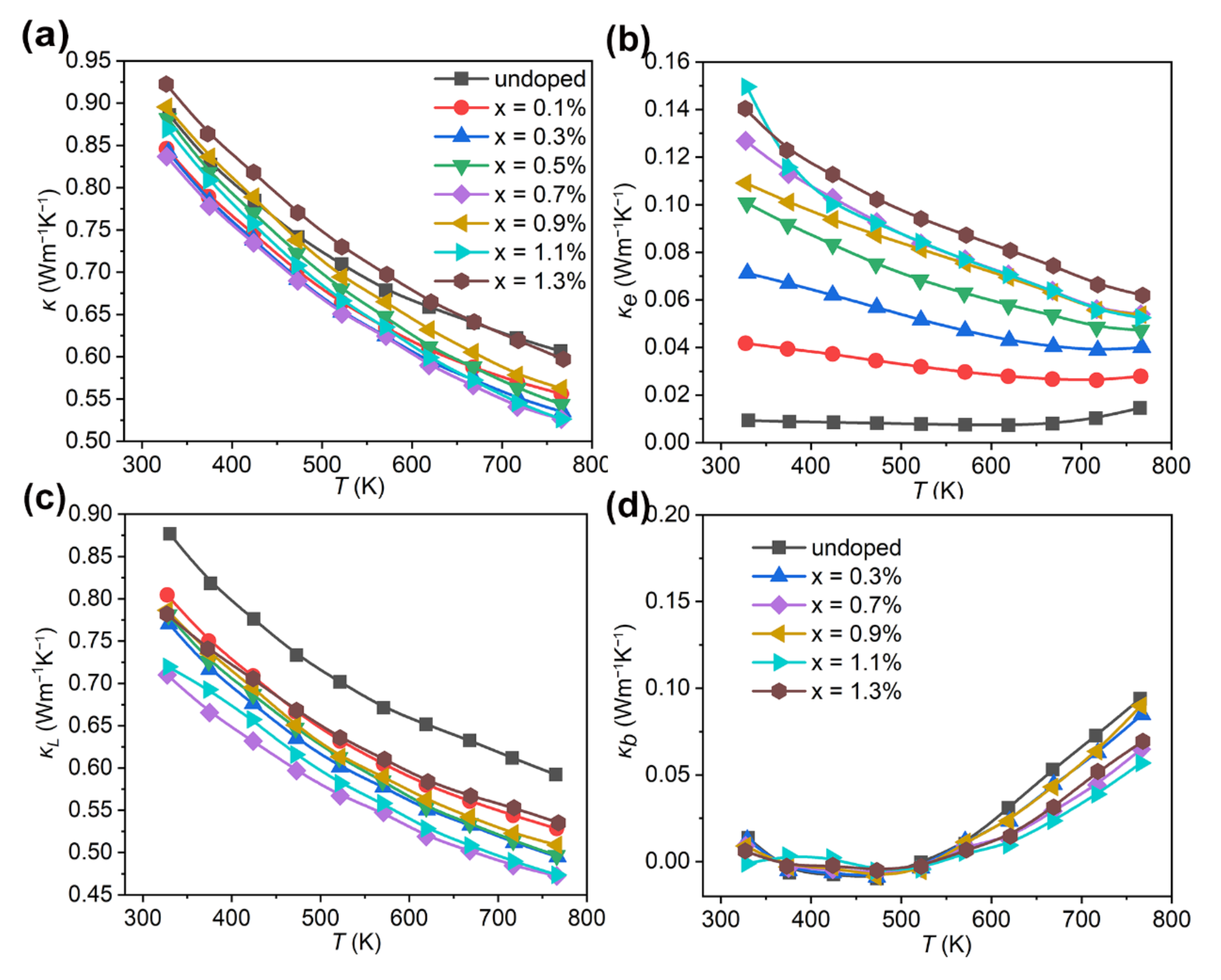
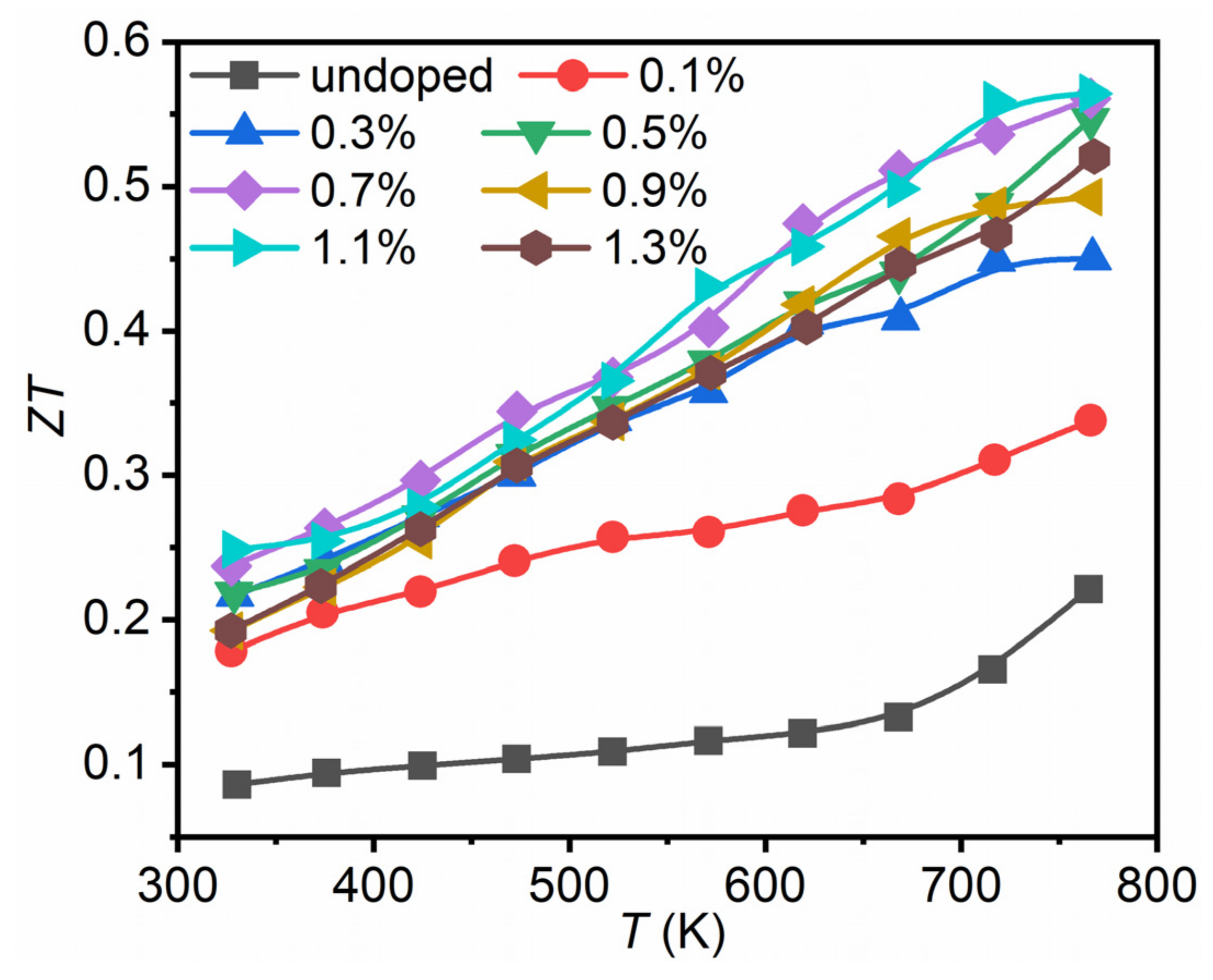
3. Results and Discussion

The XRD patterns for pristine and doped Bi2Se1−xIxS2 (x = 0–1.3%) samples are presented in Figure 1a. The main peaks agree with the standard XRD peaks of Bi2SeS2 polycrystalline, simulated from the atomic site occupation and lattice parameters a = 11.5044 Å, b = 4.0254 Å, and c = 11.2959 Å, as reported previously [19]. Reitveld refinement studied the doping-induced structural changes in the Bi2SeS2 system further (representative result is shown in Figure 1b). The XRD peaks of all samples match well with an orthorhombic Pnma phase. No phase transition can be found as the reported Br doped samples [28]. Figure 1c shows the I dopant-induced lattice parameter evolution, which was derived from the Reitveld refinement. According to the calculated formation energy [28], I preferentially occupies the Se site when doping in Bi2SeS2. The ionic radius of I (2.2 Å) exceeds Se2− (1.98 Å), which should enlarge the lattice parameters. However, no obvious changes were observed for the three axes (Figure 1c), although slight increase in the a- and c-axes appears at high doping levels. One possible reason might stem from the low doping levels of I, which cannot cause these changes. Another reason might be ascribed to the volatilization of S, which may offset lattice parameters increases caused by I doping. In addition, a weak impurity peak appeared at ~29.21° in all samples, which corresponded to the BiSe (PDF#42-1045) phase as BiSe has a characteristic peak around this position. This impurity was commonly observed in previous reports for Bi2SeS2 systems and is thought to spontaneously form due to thermodynamic stability similar to Bi2SeS2 [29].
SEM pictures for the freshly fractured surface perpendicular to the press direction at different x doping levels are shown in Figure 2a–f. All samples show very dense microstructures, which resulted in a relatively high average density of 7.07 gcm−3 and very close to the theoretical value (7.12 gcm−3). Grain sizes in the tens of microns range for the undoped sample dropped to 2–5 μm when doped with I, which indicated that iodine inhibited the diffusion of the elements during sintering and prevented the grain growth. The grains are in a lamellar structure and an apparent orientation arrangement was seen in some areas, which suggested a preferential orientation. The composition and the distribution of Bi, S, Se, and I were detected by EDS on the polished surface. In a few areas, a sulfur deficiency was observed as shown in Figure 2h, and associated with the lighter contrast area indicated as [1] in the BES image of Figure 2g, which confirmed that BiSe precipitates formed in the matrix of Bi2Se1−xIxS2 (x = 0–1.3%) as mentioned in the XRD results. Iodine was homogeneously distributed in lower doped samples (x < 1.1%), but some areas of iodine enrichment were observed at elevated dopant levels (1.1% and 1.3%, Figure 2h), which indicated that some I did not enter the lattice and x = 1.1% could represent the iodine doping limit in Bi2SeS2. Furthermore, a corresponding enrichment of Bi appeared in very few areas for those two samples indicated as [2] in Figure 2h. This might be due to lower Se levels with increasing x in Bi2Se1−xIxS2, and decreased sulfur due to the volatilization, causing excess Bi to precipitate. No Bi or I nanoprecipitate peaks were observed in the XRD patterns, mainly because of their extremely low content.
The temperature dependent electrical conductivity (σ), Seebeck coefficient (S), and power factor (PF) for Bi2Se1−xIxS2 (x = 0–1.3%) are shown in Figure 3a–c. Figure 3d presents the lattice parameters variation as a function of doping amount at room temperature. The pristine Bi2SeS2 sample has a poor σ (20.4 Scm−1) due to its low carrier concentration (n) (Figure 3a) and moderate S (350–400 μVK−1) (Figure 3b), which resulted in a low PF (<2.5 μWm−1K−2) as shown in Figure 3c. However, an obviously enhanced σ, up to 100 Scm−1, at 300 K was obtained for Bi2Se1−xIxS2 (x = 0.1%), five times higher than the undoped one. The σ roughly increases with increased doping levels (Figure 3d). For instance, increasing the doping levels from 0.3%, 0.5%, and 0.7% improved the σ from 146.3, 202.8 and 253.7 Scm−1 (Figure 3d), respectively. This value maximized at 302 Scm−1 for the 1.1% sample, although it dropped slightly for Bi2Se1−xIxS2 (x = 0.9%). Increasing x to 1.3% lowered the σ at room temperature. But from 300–773 K, the σ of Bi2Se1−xIxS2 (x = 1.3%) was better than the others (Figure 3a). As for the temperature-dependent σ, the σ for all doped samples decreased monotonically up to 773 K, which indicated a degenerate semiconductor. However, all data from doped samples exceeded the pristine sample.
The σ was determined by the carrier concentration (n) and carrier mobility (μ) based on the expression of σ = neμ, where e represents the electron charge. Figure 4a shows n and μ as a function of the doping level at room temperature. The pristine sample has a low n of 5.97 × 1018 cm−3 caused by S vacancies as follows.
Bi 2 SeS 2   xS + xV S 2 + + 2 xe
The upward arrow indicates sulfur volatilization. V S 2 + represents an S vacancy. e represents an electron. The x in Equation (1) represents the possible amount of S volatilization for the undoped sample. After doping with a small amount of I (x = 0.1%), σ increased to 2.52 × 1019 cm−3. With further increases of the doped content x to 0.3%, 0.5% and 0.7%, the n gradually increased to 3.97 × 1019 cm−3, 5.47 × 1019 cm−3 and 9.55 × 1019 cm−3, and maximized at 11.7 × 1019 cm3 when the doped content was 0.9%. This enhancement should be caused by the carrier provider of Ise, according to the following defect chemistry reaction.
Bi 2 Se 1 x S 2 I x xI Se + + xe
The I Se + indicates the replacement of Se by I in the lattice. More electron carriers were supplied if the iodine replaced Se in Bi2SeS2, which indicated I was an efficient dopant. This also confirmed that most iodine entered the lattice although some volatilized during sintering. Further increasing the doping levels to x = 1.1% and 1.3% caused the n to decrease to 8.41 × 10¹⁹ and 7.65 × 1019 cm−3. As mentioned above, I doping reaches the doping limit at x = 1.1%. In this situation, excessive levels of I can form nanoprecipitates as secondary phases. The interfaces between the secondary phases can significantly filter or block the electron carriers, which lowered n. The μ changes with increasing doping levels as shown in Figure 4a. Firstly, the value of μ slightly increases from 21.1 cm2V−1s−1 for the pristine sample to 22.2 cm2V−1s−1 and 23.5 cm2V−1s−1 when the sample doped with small amounts of x = 0.1% and 0.3%. It then decreases to 22.5, 15.5 and 12.7 cm2V−1s−1 with further increasing of the doped content x to 0.5%, 0.7% and 0.9%. Since n improved after iodine doping, the carrier-carrier scattering might be one of the scattering mechanisms causing the change of μ. In addition, the lattice imperfections introduced by I doping, impurity phases, and their phase boundaries could further scatter the carriers, which also play an important role in the carrier scattering. For samples doped with x = 1.1% and 1.3%, μ increases to 19.2 and 20 cm2V−1s1 due to reduced carrier scattering, since the iodine doping reaches its limit as mentioned above. Moreover, grain sizes for samples doped with x = 1.1% and 1.3% increased as compared to samples with lower doped levels as shown in Figure 2, which also reduces carrier scattering because of the decreased grain boundary concentration. Combined with the n data, the increase of σ for the doped samples primarily resulted from the increase of n, while the reduced data for the doped sample with x = 0.9% was attributed to the reduced μ. Moreover, the improved σ and n for samples doped with x < 1.1% indicated that electron doping (I) successfully occurred in the Bi2SeSe2 system.
Figure 3b shows the Seebeck coefficient (S) for Bi2Se1−xIxS2 (x = 0–1.3%). The negative data over the entire temperature range suggested that Bi2SeS2 is an n-type semiconductor. Overall, the S for all doped samples improved with a temperature increase. The pristine Bi2SeS2 sample shows a relatively high S ~350 μVK−1 at room temperature. After iodine doping, the value dropped due to the enhanced carrier concentration. It gradually dropped to 148 μVK−1 as the doping level increased to 1.3%. According to the Mott formula [34], S can be expressed by the following equation:
S = 8 π k B 2 T 3 e h 2 m * π 3 n 2 3                
where kB, h, e, m* and n are the Boltzmann constant, the Planck constant, the electronic charge, the electron effective mass at the Fermi level, and the carrier concentration, respectively. This means increasing n would decrease S. In addition, an increase of m* should increase the S. To present a quantitative understanding of the microscopic carrier variations, densities of state effective mass m* are derived. Assuming that electron conduction occurs within a single parabolic band (SPB) with scattering dominated by the acoustic phonon model, the change of S with n can be plotted using the equations described elsewhere [33,35,36,37]. Herein, the relationship between S with the n is called the Pisarenko relation [33]. The solid curve of the SPB model fitted for the S(n) function is shown in Figure 4b. The Pisarenko relationship fitted well with an m* of 1.7mo, where mo is the electron mass, and indicates the band structure was not changed by I substitution. Herein, the m* of Bi2SeS2 was larger than Bi2S3 (~1.5mo) [38], which seems the key factor leading to the higher S but lower μ of Bi2SeS2.
Figure 3c gives the power factor (PF). Since the enhanced σ for the doped samples completely compensated for the S decline, the resultant PF enhanced significantly. A maximum PF of 697 μWm−1K−2 was achieved for Bi2Se1−xIxS2 (x = 1.1%) at 300 K, three times higher than the undoped sample, and larger than other reported data of Bi2SeS2 + CuI (<500 μWm−1K−2 at 300 K), Bi2S3 (<100 μWm−1K−2 at 300 K) and Bi2Se3 (<200 μWm−1K−2 at 300 K) [19,20,39].
Figure 5a shows the total thermal conductivity (κ) for Bi2Se1−xIxS2 (x = 0–1.3%). The pristine Bi2SeS2 shows a low κ of 0.88 Wm−1K−1 at 300 K, which decreased further to 0.60 Wm−1K−1 at 773 K. This intrinsically low κ of Bi2SeS2 was due to its layered structure with weak bonding strength, because it acts as a boundary for effective phonon scattering sources in the Bi2SeS2 matrix [40]. The κ of the doped samples Bi2Se1−xIxS2 with x = 0.1%, 0.3%, 0.5%, 0.7%, 0.9% and 1.1% were all lower compared to the undoped sample. The lowest κ values of 0.83 Wm−1K−1 at room temperature and 0.52 Wm−1K−1 at 773 K were obtained for Bi2Se1−xIxS2 (x = 0.7%). Due to the high electronic thermal conductivity (κe), discussed below, the κ of Bi2Se1−xIxS2 (x = 1.3%) was slightly higher than the undoped sample.
Generally, the κ is the sum of the lattice thermal conductivity (κL) and the electronic thermal conductivity (κe), depicted below:
κ = κ   e + κ L  
The κe was obtained through the Wiedemann–Franz relationship, κe = LσT, where σ, T, and L are the electrical conductivity, temperature, and the Lorenz number, respectively. Here, the L ranges from 1.50 × 10⁻⁸ to 1.80 × 10⁻⁸ ΩWK−2, which is calculated by applying the reduced Fermi energy η. The κe for Bi2Se1−xIxS2 (x = 0–1.3%) is presented in Figure 5b. After doping with I, the κe increased due to the increased σ. It gradually improved with higher dopant levels. However, the κe holds only 5~17% of the κ for all doped samples, indicating that the κ is not predominated by κe. The temperature dependence of κL is shown in Figure 5c. κL decreased significantly over the entire temperature range after doping. At room temperature, this parameter dropped from 0.87 Wm−1K−1 for the pristine sample to 0.78 Wm−1K−1 for Bi2Se1−xIxS2 (x = 0.3%), to 0.77 Wm−1K−1 for Bi2Se1−xIxS2 (x = 0.5%), and further to 0.71 Wm−1K−1 for Bi2Se1−xIxS2 (x = 0.7%). The significant κL reduction should result from the enhanced phonon scattering from the secondary phase of BiSe and the heavier relative atomic mass of I because it introduces strong phonon scattering due to the mass fluctuations. In addition, the increased grain boundary concentration caused by the reduced grain size after doping (Figure 2) also played an important role in phonon scattering. Further increasing the dopant to 0.9%, 1.1% and 1.3%, the κL increased slightly compared with other doped samples. One possible reason may be due to the redundancy of Bi-rich nano-precipitates with a relatively higher κL in the sample. Another possible reason may be the reduced grain boundary scattering due to the reduced grain boundary concentration and the increased grain size for high-doped samples. As shown in Figure 2, the grain size for the undoped sample decreased with iodine doping. However, with upping the dopant level to 0.9%, the grain size increased. The Bi-rich nano-precipitates might act as a sintering aid, contributing to the sample grain growth [41]. As for the data dependence of the temperature, the κL for all samples decreased with increasing temperature. However, above 600 K, the value decreases slowly. This should be attributed to the bipolar effect. In fact, for a wide-gap semiconductor at elevated temperatures or narrow-gap semiconductor at room temperature, both holes and electrons contribute to transport. This indicates that bipolar thermal conductivity (κb) should be considered. The κb was separated from κ to clarify the contribution of κb at high temperatures, according to the method reported by Kitagawa et al. [42]. Figure 5d shows the κb for some representative samples. It shows that κb has been reduced for the doped samples. It dropped from 0.094 Wm−1K−1 to 0.056 Wm−1K−1 for doped levels from x = 0 to x = 1.1% at 773 K, likely due to the trapping of minority carriers within the dense nanoscale regions [28]. Thus, although κe increased due to n optimization, the total thermal conductivity dropped by reducing κL and suppressing κb. These results indicated iodine dopants synergistically regulated the electrical and thermal transport properties of Bi2SeS2.
Figure 6 shows the ZT values for Bi2Se1−xIxS2 (x = 0–1.3%). Combining with the optimized power factor and reduced thermal conductivity, a maximum ZT value of 0.56 at 773 K was obtained for Bi2Se1−xIxS2 (x = 1.1%), nearly three times higher than undoped Bi2SeS2, and indicating that iodine is an effective n-type dopant for Bi2SeS2. However, compared with Br doped samples [28], the present ZT value was much lower due to the degraded power factor at high temperatures. Further efforts can be devoted to the enhancement of the electrical transport properties of Bi2SeS2 at high temperature, such as dual-doping.

4. Conclusions

A series of Bi2Se1−xIxS2 (x = 0–1.3%) samples were prepared by combining a solid state reaction with SPS. Those results revealed that iodine is an effective n-type dopant for Bi2SeS2. The electrical conductivity increased due to optimized carrier concentration produced by the carrier provided defect Ise. Combined with a moderate Seebeck coefficient (>150 µVK−1) due to its large effective mass, a high power factor of 697 μWm−1K−2 at 300 K was obtained. In addition, the total thermal conductivity decreased, primarily due to the decreased lattice thermal conductivity resulting from the enhanced phonon scattering. Thus, a maximum ZT of 0.56 at 773 K was achieved for Bi2Se1−xIxS2 (x = 1.1%), nearly three times higher than the pristine sample.

Author Contributions

Conceptualization, F.L.; methodology, C.L. (Chongbin Liang) and B.J.; validation, F.L. and Y.C.; formal analysis, C.L. (Chongbin Liang) and C.L. (Chen Liu); investigation, C.L. (Chongbin Liang) and B.J.; data curation, C.L. (Chongbin Liang) and Z.Z.; writing—original draft preparation, C.L. (Chongbin Liang); writing—review and editing, B.J. and F.L.; supervision, P.F. All authors have read and agreed to the published version of the manuscript.

Funding

This work was supported by the National Natural Science Foundation of China (No. 52072248), Natural Science Foundation of Guangdong Province of China (No. 2021A1515012128, No. 2018A030313574) and Natural Science Foundation of SZU (No. 827-000357).

Institutional Review Board Statement

Not applicable.

Informed Consent Statement

Not applicable.

Data Availability Statement

The data presented in this study are available on request from the corresponding author.

Conflicts of Interest

The authors declare no conflict of interest.

References

  1. Bérardan, D.; Guilmeau, E.; Maignan, A.; Raveau, B. In2O3: Ge, a promising n-type thermoelectric oxide composite. Solid State Commun. 2008, 146, 97–101. [Google Scholar] [CrossRef]
  2. Chen, G.; Dresselhaus, M.S.; Dresselhaus, G.; Fleurial, J.P.; Cailla, T. Recent developments in thermoelectric materials. Int. Mater. Rev. 2003, 48, 45–66. [Google Scholar] [CrossRef]
  3. Bell, L.E. Cooling, heating, generating power, and recovering waste heat with thermoelectric systems. Science 2008, 321, 1457–1461. [Google Scholar] [CrossRef] [PubMed] [Green Version]
  4. DiSalvo, F.J. Thermoelectric cooling and power generation. Science 1999, 285, 703–706. [Google Scholar] [CrossRef]
  5. Rowe, D.M. CRC Handbook of Thermoelectrics; CRC Press: Boca Raton, FL, USA, 1995. [Google Scholar]
  6. Nolas, G.S. Basic Principles and New Materials Developments; Springer: New York, NY, USA, 2001. [Google Scholar]
  7. Zhang, X.; Zhao, L.D. Thermoelectric materials: Energy conversion between heat and electricity. J. Mater. 2015, 1, 92–105. [Google Scholar] [CrossRef] [Green Version]
  8. Yang, L.; Chen, Z.G.; Dargusch, M.S.; Zou, J. High performance thermoelectric materials: Progress and their applications. Adv. Energy Mater. 2018, 8, 6. [Google Scholar] [CrossRef]
  9. Slack, G. New Materials and Performance Limits for Thermoelectric Cooling; CRC: Boca Raton, FL, USA, 1995. [Google Scholar]
  10. Pei, Y.; Shi, X.; LaLonde, A.; Wang, H.; Chen, L.; Snyder, G.J. Convergence of electronic bands for high performance bulk thermoelectric. Nature 2011, 473, 66–69. [Google Scholar] [CrossRef]
  11. Heremans, J.P.; Thrush, C.M.; Morelli, D.T. Thermopower enhancement in lead telluride nanostructures. Phys. Rev. B 2004, 70, 11–15. [Google Scholar] [CrossRef]
  12. Liu, H.L.; Yuan, X.; Lu, P.; Shi, X.; Xu, F.F.; He, Y.; Tang, Y.S.; Bai, S.Q.; Zhang, W.Q.; Chen, L.D.; et al. Ultrahigh thermoelectric performance by electron and phonon critical scattering in Cu2Se1−xIx. Adv. Mater. 2013, 25, 6607–6612. [Google Scholar] [CrossRef] [Green Version]
  13. Biswas, K.; He, J.; Blum, I.D.; Wu, C.I.; Hogan, T.P.; Seidman, D.N.; Dravid, V.P.; Kanatzidis, M.G. High-performance bulk thermoelectrics with all-scale hierarchical architectures. Nature 2012, 489, 414–418. [Google Scholar] [CrossRef]
  14. Liu, W.S.; Zhang, Q.; Lan, Y.; Chen, S.; Yan, X.; Zhang, Q.; Wang, H.; Wang, D.; Chen, G.; Ren, Z. Thermoelectric property studies on Cu-doped n-type CuxBi2Te2.7Se0.3 nanocomposites. Adv. Energy Mater. 2011, 1, 577–587. [Google Scholar] [CrossRef]
  15. Finefrock, S.W.; Yang, H.; Fang, H.; Wu, Y. Thermoelectric properties of solution synthesized nanostructured materials. Annu. Rev. Chem. Biomol. Eng. 2015, 6, 247–266. [Google Scholar] [CrossRef]
  16. Hu, L.P.; Zhu, T.J.; Wang, Y.G.; Xie, H.H.; Xu, Z.J.; Zhao, X.B. Shifting up the optimum figure of merit of p-type bismuth telluride-based thermoelectric materials for power generation by suppressing intrinsic conduction. NPG Asia Mater. 2014, 6, e88. [Google Scholar] [CrossRef] [Green Version]
  17. Ge, Z.H.; Zhao, L.D.; Wu, D.; Liu, X.Y.; Zhang, B.P.; Li, J.F.; He, J.Q. Low-cost, abundant binary sulfides as promising thermoelectric materials. Mater. Today 2016, 19, 227–239. [Google Scholar] [CrossRef]
  18. Farooq, M.U.; Butt, S.; Gao, K.W.; Sun, X.G.; Pang, X.L.; Khan, S.U.; Xu, W.; Mohmed, F.; Mahmood, A.; Mahmood, N. Enhanced thermoelectric efficiency of Cu2−xSe-Cu2S composite by incorporating Cu2S nanoparticles. Ceram. Int. 2016, 42, 8395–8401. [Google Scholar] [CrossRef]
  19. Liu, W.S.; Lukas, K.C.; McEnaney, K.; Lee, S.; Zhang, Q.; Opeil, C.P.; Chen, G.; Ren, Z.F. Studies on the Bi2Te3-Bi2Se3-Bi2S3 system for mid-temperature thermoelectric energy conversion. Energy Environ. Sci. 2013, 6, 552–560. [Google Scholar] [CrossRef]
  20. Ge, Z.H.; Qin, P.; He, D.S.; Chong, X.Y.; Feng, D.; Ji, Y.H.; Feng, J.; He, J.Q. Highly enhanced thermoelectric properties of Bi/Bi2S3nanocomposites. ACS Appl. Mater. Inter. 2017, 9, 4828–4834. [Google Scholar] [CrossRef]
  21. Biswas, K.; Zhao, L.D.; Kanatzidis, M.G. Tellurium-free thermoelectric: The anisotropic n-type semiconductor Bi2S3. Adv. Energy Mater. 2012, 2, 634–638. [Google Scholar] [CrossRef]
  22. Ge, Z.H.; Zhang, B.P.; Shang, P.P.; Li, J.F. Control of anisotropic electrical transport property of Bi2S3 thermoelectric polycrystals. J. Mater. Chem. 2011, 21, 9194–9200. [Google Scholar] [CrossRef]
  23. Chen, Y.; Wang, D.Y.; Zhou, Y.L.; Pang, Q.T.; Shao, J.W.; Wang, G.T.; Wang, J.F.; Zhao, L.D. Enhancing the thermoelectric performance of Bi2S3: A promising earth abundant thermoelectric material. Front. Phys. 2019, 14, 13601. [Google Scholar] [CrossRef]
  24. Kawamoto, Y.; Iwasaki, H. Thermoelectric properties of (Bi1−xSbx)2S3 with orthorhombic structure. J. Electron. Mater. 2014, 43, 1475. [Google Scholar] [CrossRef]
  25. Zhao, L.D.; Zhang, B.P.; Liu, W.S.; Zhang, H.L.; Li, J.F. Enhanced thermoelectric properties of bismuth sulfide polycrystals prepared by mechanical alloying and spark plasma sintering. J. Solid State Chem. 2008, 181, 3278–3282. [Google Scholar] [CrossRef]
  26. Ge, Z.H.; Zhang, B.P.; Li, J.F. Microstructure composite-like Bi2S3 polycrystals with enhanced thermoelectric properties. J. Mater. Chem. 2012, 22, 17589–17594. [Google Scholar] [CrossRef]
  27. Li, F.; Ruan, M.; Jabar, B.; Liang, C.B.; Chen, Y.X.; Ao, D.W.; Zheng, Z.H.; Fan, P.; Liu, W.S. High thermoelectric properties achieved in environmentally friendly sulfide compound Bi2SeS2 by nanoenginnering. Nano Energy 2021, 88, 106273. [Google Scholar] [CrossRef]
  28. Jabar, B.; Li, F.; Zheng, Z.H.; Mansoor, A.; Zhu, Y.B.; Liang, C.B.; Ao, D.W.; Chen, Y.X.; Liang, G.X.; Fan, P.; et al. Homo-composition and hetero-structure nanocomposite Pnma Bi2SeS2Pnnm Bi2SeS2 with high thermoelectric performance. Nat. Commun. 2021, 12, 7192. [Google Scholar] [CrossRef]
  29. Li, L.; Liu, Y.; Dai, J.Y.; Zhu, H.X.; Hong, A.J.; Zhou, X.H. Thermoelectric property studies on CuxBi2SeS2 with nano-scale precipitates Bi2S3. Nano Energy 2015, 12, 447–456. [Google Scholar] [CrossRef] [Green Version]
  30. Ruan, M.; Li, F.; Chen, Y.X.; Zheng, Z.H.; Fan, P. Te-free compound Bi2SeS2 as a promising mid-temperature thermoelectric material. J. Alloys Compd. 2020, 849, 156677. [Google Scholar] [CrossRef]
  31. Liu, Z.; Pei, Y.; Geng, H.; Zhuo, J.; Meng, X.; Cai, W.; Liu, W.; Sui, J. Enhanced thermoelectric properties of Bi2S3 by synergistically action of bromine substitution and copper nanoparticles. Nano Energy 2015, 13, 554–562. [Google Scholar] [CrossRef]
  32. Ji, W.; Shi, X.L.; Liu, W.; Yuan, H.; Zheng, K.; Wan, B.; Shen, W.; Zhang, Z.; Fang, C.; Wang, Q.; et al. Boosting the thermoelectric performance of n-type Bi2S3 by hierarchical structure manipulation and carrier density optimization. Nano Energy 2021, 87, 106171. [Google Scholar] [CrossRef]
  33. Wei, T.R.; Wang, H.; Gibbs, Z.M.; Wu, C.F.; Snyder, G.J.; Li, J.F. Thermoelectric properties of Sn-doped p-type Cu3SbSe4: A compound with large effective mass and small band gap. J. Mater. Chem. A 2014, 2, 13527–13533. [Google Scholar] [CrossRef] [Green Version]
  34. Snyder, G.J.; Toberer, E.S. Complex thermoelectric materials. Nat. Mater. 2008, 7, 105–114. [Google Scholar] [CrossRef] [PubMed] [Green Version]
  35. Pichanusakorn, P.; Bandaru, P.R. Minimum length scales for enhancement of the power factor in thermoelectric nanostructures. J. Appl. Phys. 2010, 107, 0743047. [Google Scholar] [CrossRef] [Green Version]
  36. Pichanusakorn, P.; Bandaru, P.R. The optimal Seebeck coefficient for obtaining the maximum power factor in thermoelectrics. Appl. Phys. Lett. 2009, 94, 22310822. [Google Scholar] [CrossRef] [Green Version]
  37. May, A.F.; Toberer, E.S.; Saramat, A.; Jeffrey Snyder, G. Characterization and analysis of thermoelectric transport in n-type Ba8Ga16−xGe30+x. Phys. Rev. B Condens. Matter Mater. Phys. 2009, 80, 125205. [Google Scholar] [CrossRef]
  38. Guo, J.; Zhang, Y.X.; Wang, Z.Y.; Zheng, F.; Ge, Z.H.; Fu, J.; Fen, J. High thermoelectric properties realized in earth-abundant Bi2S3 bulk via carrier modulation and multi-nano-precipitates synergy. Nano Energy 2020, 78, 105227. [Google Scholar] [CrossRef]
  39. Hor, Y.S.; Richardella, A.; Roushan, P.; Xia, Y.; Checkelsky, J.G.; Yazdani, A.; Hasan, M.Z.; Ong, N.P.; Cava, R.J. P-type Bi2Se3 for topological insulator and low temperature thermoelectric applications. Phys. Rev. B 2009, 79, 195208. [Google Scholar] [CrossRef] [Green Version]
  40. Yang, L.; Chen, Z.G.; Hong, M.; Han, G.; Zou, J. Enhanced thermoelectric performance of nanostructured Bi2Te3 through significant phonon scattering. ACS Appl. Mater. Inter. 2015, 7, 23694–23699. [Google Scholar] [CrossRef]
  41. Zheng, Z.H.; Wang, T.; Jabar, B.; Ao, D.W.; Li, F.; Chen, Y.X.; Liang, G.X.; Luo, J.T.; Fan, P. Enhanced thermoelectric performance in n-type Bi2O2Se by an exquisite grain boundary engineering approach. ACS Appl. Energy Mater. 2021, 4, 10290–10297. [Google Scholar] [CrossRef]
  42. Kitagawa, H.; Wakatsuki, M.; Nagaoka, H.; Noguchi, H.; Isoda, Y.; Hasezaki, K.; Noda, Y. Temperature dependence of thermoelectric properties of Ni-doped CoSb3. J. Phys. Chem. Solids 2005, 66, 1635–1639. [Google Scholar] [CrossRef]
Figure 1. (a) XRD patterns for Bi2Se1−xIxS2 (x = 0–1.3%). The asterisk represents the impurity peak of BiSe. (b) Rietveld refinement analysis from XRD patterns of Bi2SeS2, where obs represents observed, calc is calculated, bkg is background, and diff is the residual difference between the curves. (c) Variation of lattice parameters with the doped amount x. (d) Crystal structure along the a-axis for the iodine doped Bi2SeS2.
Nanomaterials 12 02434 g001
Figure 2. (af) SEM pictures of fresh fracture surfaces for Bi2Se1−xIxS2 with x = 0, 0.1%, 0.3%, 0.5%, 0.9%, and 1.3%; (g) BES image for Bi2Se1−xIxS2 (x = 1.3%). The lighter contrast areas are indicated as 1, while the deep contrast areas are indicated as 2; (h) Distribution of the corresponding elements Bi, Se, S and I on the sample surface in (g).
Nanomaterials 12 02434 g002
Figure 3. Temperature dependence of (a) electrical conductivity (σ), (b) Seebeck coefficient (S) and (c) power factor (PF) for Bi2Se1−xIxS2 (x = 0–1.3%). (d) Change of electrical transport parameters (σ, S and PF) with doping level at room temperature.
Nanomaterials 12 02434 g003
Figure 4. (a) Change of carrier concentration (n) and carrier mobility (μ) with doping content x, (b) Change of Seebeck coefficient (S) with carrier concentration (n). The line in (b) was calculated by the SPB model discussed in detail elsewhere [28,33]. m* is the electron effective mass at the Fermi level.
Nanomaterials 12 02434 g004
Figure 5. Thermal transport properties for Bi2Se1−xIxS2 (x = 0–1.3%). (a) Total thermal conductivity (κ), (b) electronic thermal conductivity (κe), (c) lattice thermal conductivity (κL), (d) bipolar thermal conductivity b).
Nanomaterials 12 02434 g005
Figure 6. Dimensionless figure of merit (ZT) for Bi2Se1−xIxS2 (x = 0–1.3%).
Nanomaterials 12 02434 g006
Publisher’s Note: MDPI stays neutral with regard to jurisdictional claims in published maps and institutional affiliations.

