
A Photoexcited Switchable Dual-Function Metamaterial Absorber for Sensing and Wideband Absorption at THz Band

Abstract
:1. Introduction
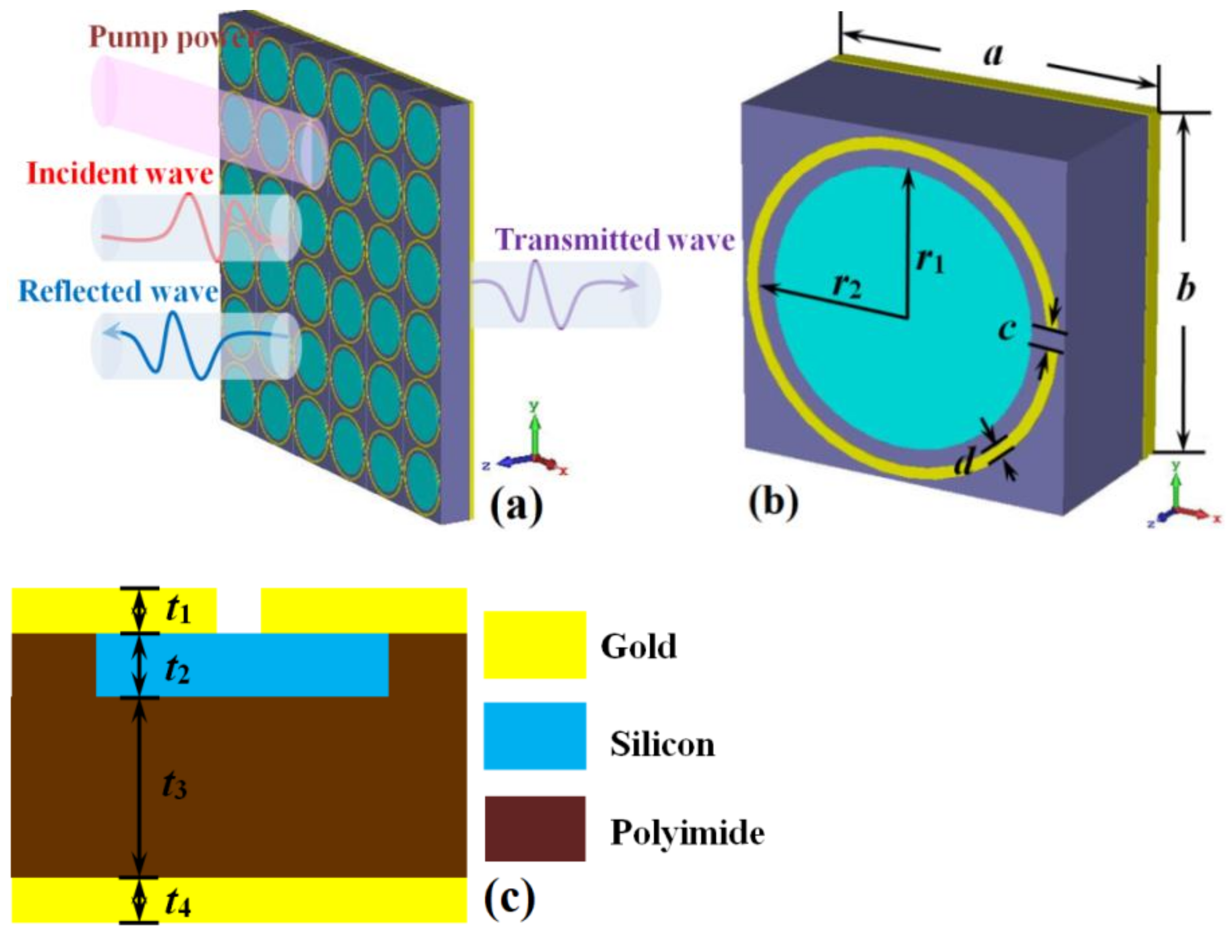
2. Model Design
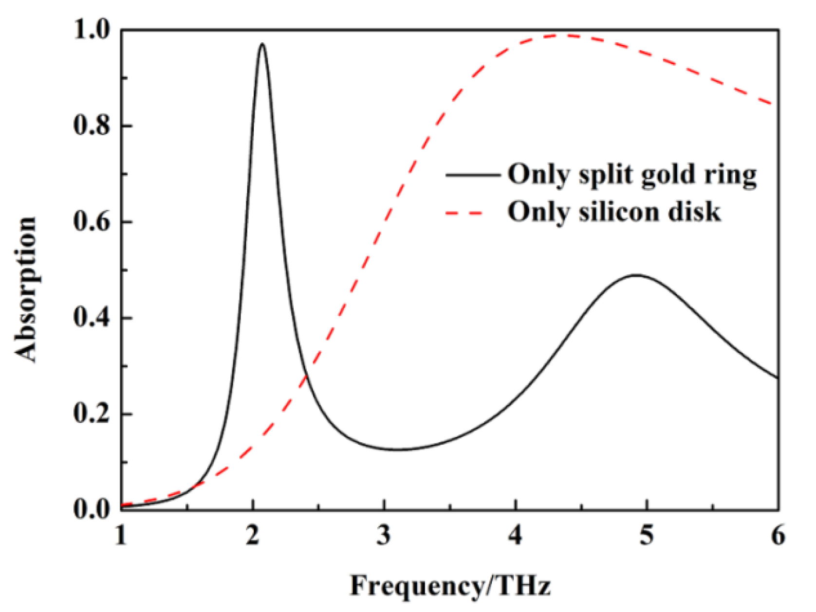
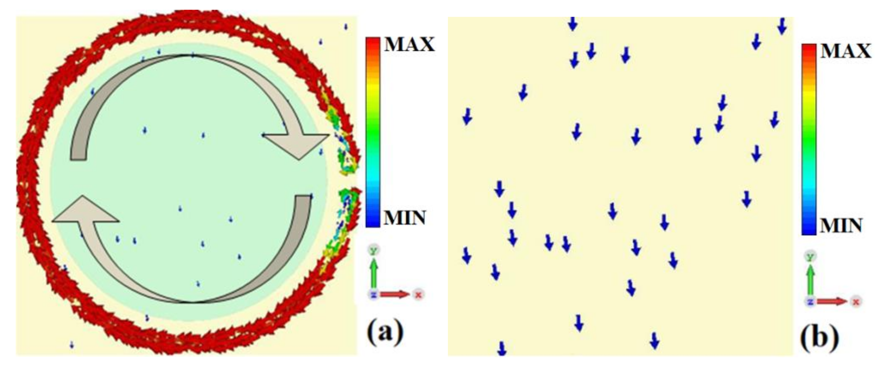
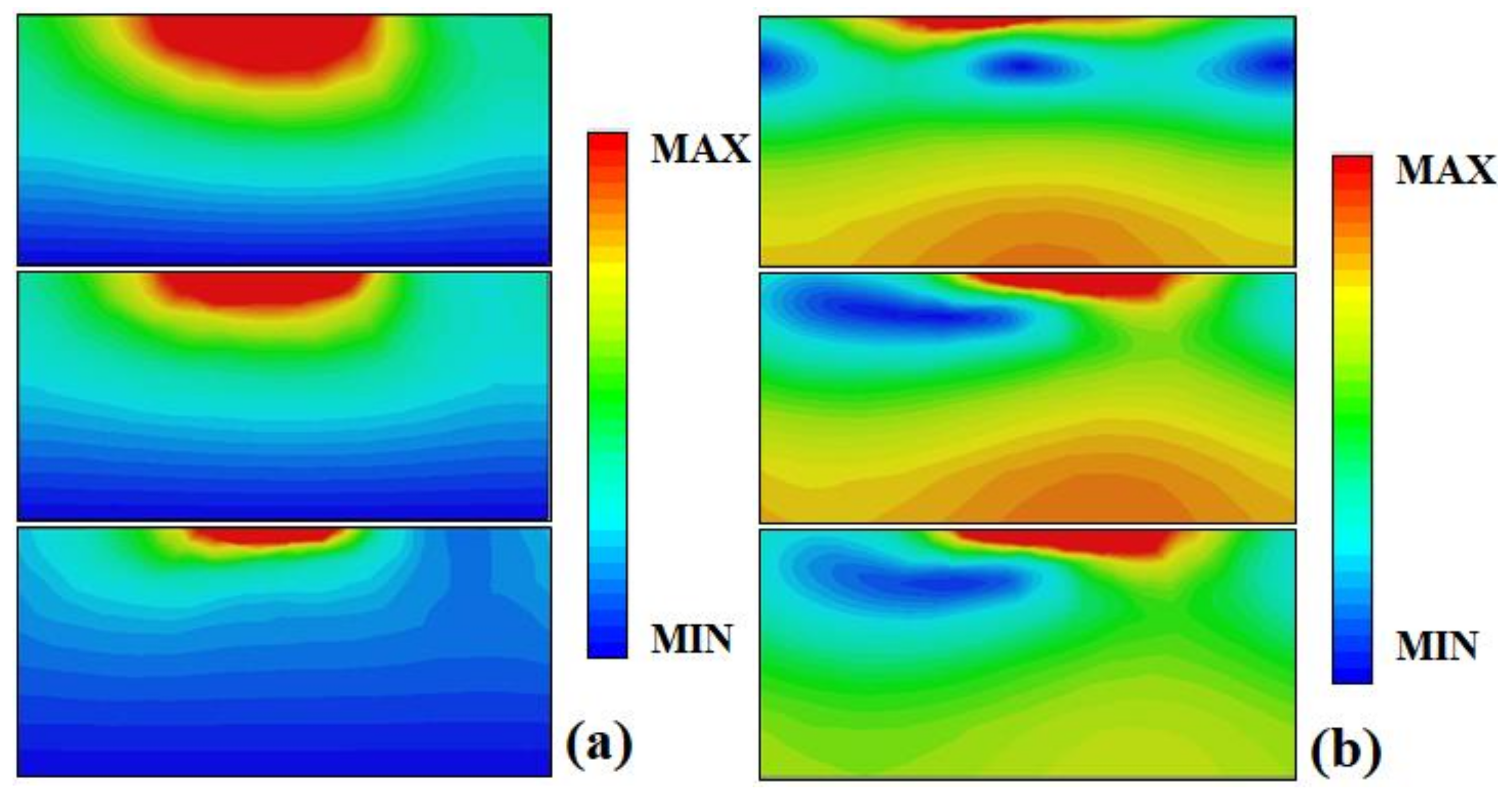
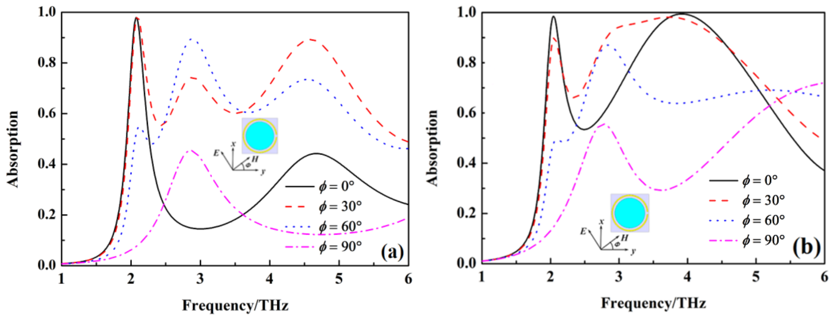
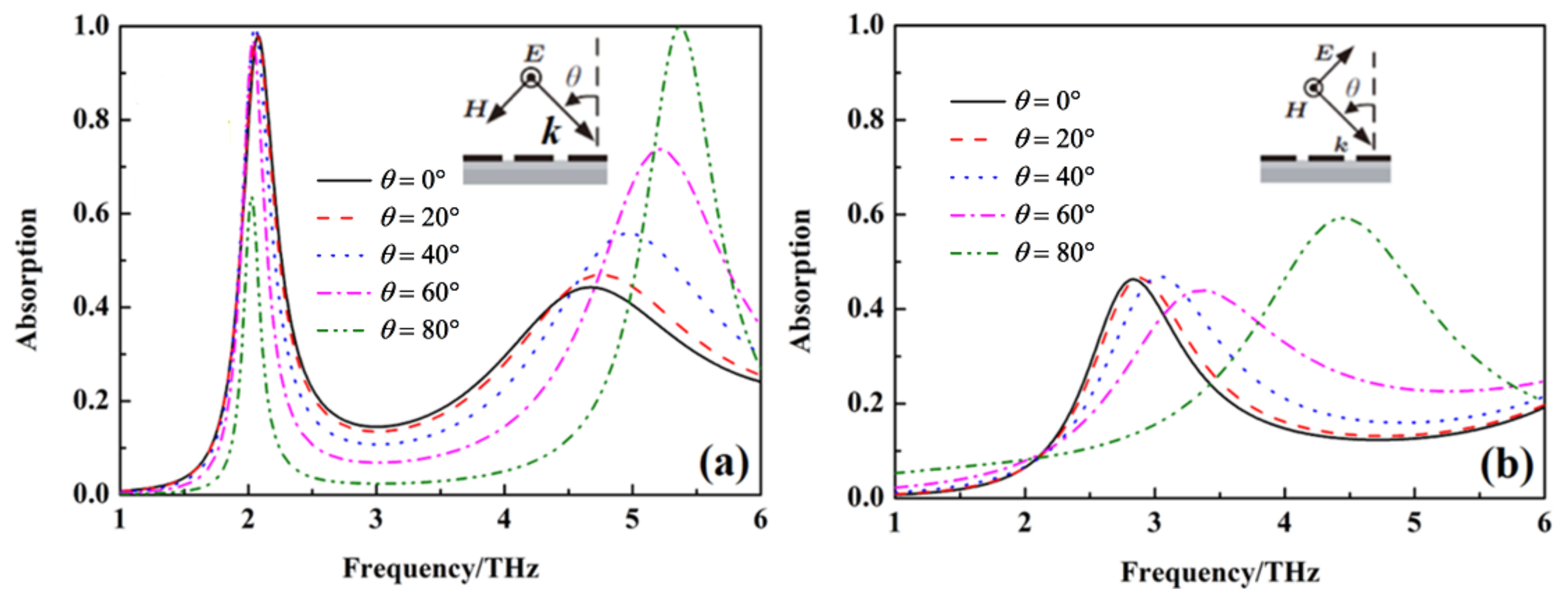
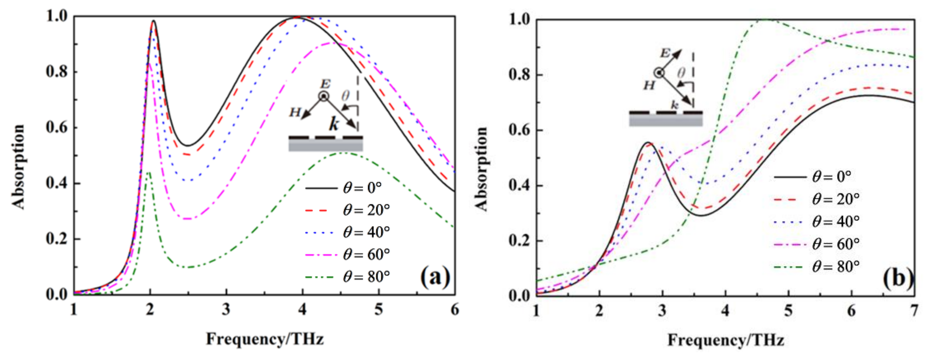
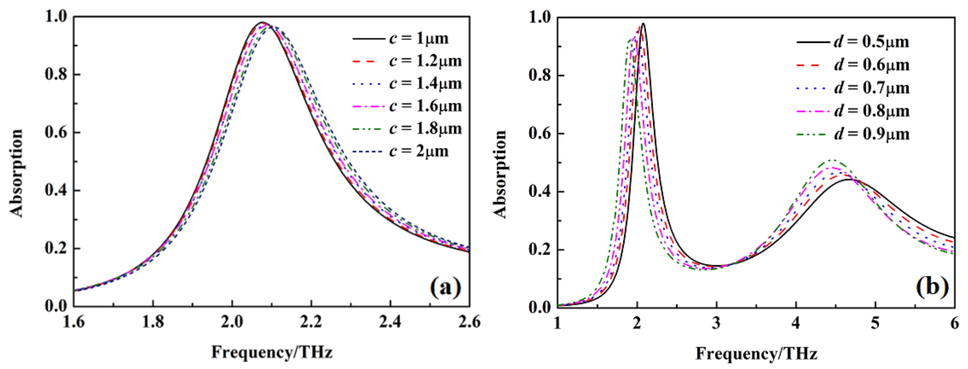
3. Results and Discussion
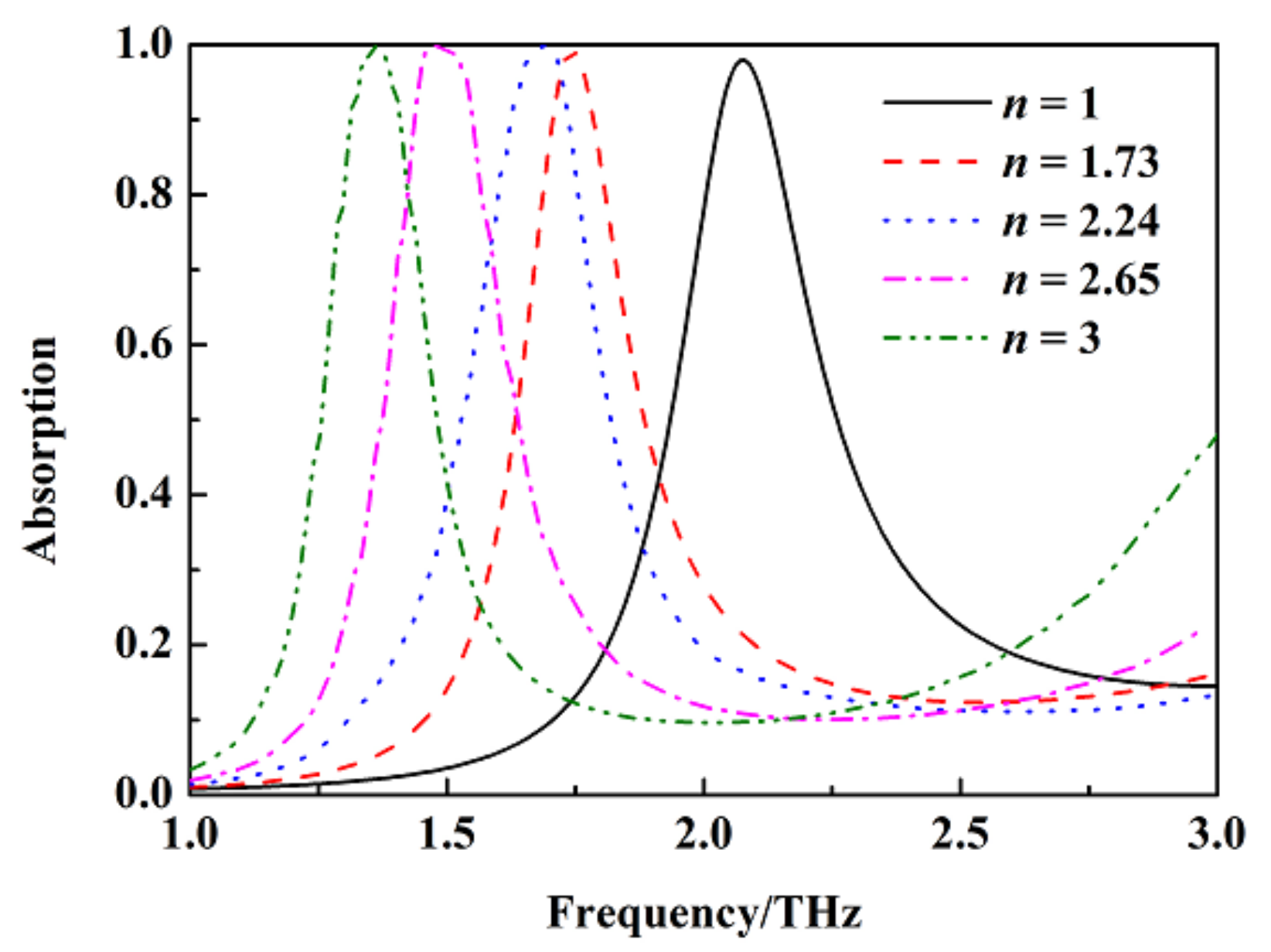
4. The Sensing Property of Metamaterial Absorber
5. Summary
Author Contributions
Funding
Institutional Review Board Statement
Informed Consent Statement
Data Availability Statement
Acknowledgments
Conflicts of Interest
References
- Withayachumnankul, W.; Abbott, D. Metamaterials in the Terahertz regime. IEEE Photon. J. 2009, 1, 99–118. [Google Scholar] [CrossRef]
- Chen, H.T.; Padilla, W.J.; Zide, J.; Gossard, A.C.; Taylor, A.J.; Averitt, R.D. Active terahertz metamaterial devices. Nature 2006, 444, 597–600. [Google Scholar] [CrossRef] [PubMed] [Green Version]
- Hu, T.; Padilla, W.J.; Zhang, X.; Averitt, R.D. Recent progress in electromagnetic metamaterial devices for Terahertz applications. IEEE J. Sel. Top. Quantum Electron 2011, 17, 92–101. [Google Scholar]
- Li, Z.F.; Liu, J.; Zhang, J.; Shao, L.D.; Zhang, C.B.; Wang, X.; Jin, R.H.; Zhu, W.R. Shaping electromagnetic fields with irregular metasurface. Adv. Mater. Technol. 2022, 7, 2200035. [Google Scholar] [CrossRef]
- Bai, X.D.; Zhang, F.L.; Sun, L.; Cao, A.J.; He, C.; Zhang, J.; Zhu, W.R. Dynamic millimeter-wave OAM beam generation through programmable metasurface. Nanophotonics 2022, 11, 1389–1399. [Google Scholar] [CrossRef]
- Zhang, C.B.; Xue, T.J.; Zhang, J.; Liu, L.H.; Xie, J.H.; Wang, G.M.; Yao, J.Q.; Zhu, W.R.; Ye, X.D. Terahertz toroidal metasurface biosensor for sensitive distinction of lung cancer cells. Nanophotonics 2022, 11, 101–109. [Google Scholar] [CrossRef]
- Li, Z.F.; Zhang, D.J.; Liu, J.; Zhang, J.; Shao, L.D.; Wang, X.; Jin, R.H.; Zhu, W.R. Three-dimensional manipulation of dual-helical electromagnetic wavefronts with a non-interleaved metasurface. IEEE Trans. Antenn. Propag. 2022, 70, 378–388. [Google Scholar] [CrossRef]
- Yang, W.X.; Chen, K.; Zheng, Y.L.; Zhao, W.B.; Hu, Q.; Qu, K.; Jiang, T.; Zhao, J.M.; Feng, Y.J. Angular-adaptive reconfigurable spin-locked metasurface retroreflector. Adv. Sci. 2021, 8, 2100885. [Google Scholar] [CrossRef]
- Luo, X.Y.; Guo, W.L.; Chen, K.; Zhao, J.M.; Jiang, T.; Liu, Y.; Feng, Y.J. Active cylindrical metasurface with spatial reconfigurability for tunable backward scattering reduction. IEEE Trans. Antenn. Propag. 2021, 69, 3332–3340. [Google Scholar] [CrossRef]
- Chen, K.; Ding, G.W.; Hu, G.W.; Jin, Z.W.; Zhao, J.M.; Feng, Y.J.; Jiang, T.; Alù, A.; Qiu, C.W. Directional Janus metasurface. Adv. Mater. 2020, 32, 1906352. [Google Scholar] [CrossRef]
- Guo, W.L.; Chen, K.; Wang, G.M.; Luo, X.Y.; Cai, T.; Zhang, C.B.; Feng, Y.J. Airy beam generation: Approaching ideal efficiency and ultra wideband with reflective and transmissive metasurfaces. Adv. Opt. Mater. 2020, 8, 2000860. [Google Scholar] [CrossRef]
- Cheng, Y.Z.; Yang, H.L.; Cheng, Z.Z.; Wu, N. Perfect metamaterial absorber based on a split-ring-cross resonator. Appl. Phys. A 2011, 102, 99–103. [Google Scholar] [CrossRef]
- Wang, B.; Koschny, T.; Soukoulis, C.M. Wide-angle and polarization independent chiral metamaterial absorbers. Phys. Rev. B 2009, 80, 033108. [Google Scholar] [CrossRef] [Green Version]
- Tao, H.; Bingham, C.M.; Strikwerda, A.C.; Pilon, D.; Shrekenhamer, D.; Landy, N.I.; Fan, K.; Zhang, X.; Padilla, W.J.; Averritt, R.D. Highly flexible wide angle of incidence terahertz metamaterial absorber: Design, fabrication, and characterization. Phys. Rev. B 2008, 78, 241103. [Google Scholar] [CrossRef]
- Wen, Q.Y.; Zhang, H.W.; Xie, Y.S.; Yang, Q.H.; Liu, Y.L. Dual band terahertz metamaterial absorber: Design, fabrication, and charac-terization. Appl. Phys. Lett. 2009, 95, 241111. [Google Scholar] [CrossRef]
- Shen, X.P.; Cui, T.J.; Zhao, J.M.; Ma, H.F.; Jiang, W.X.; Liu, H. Polarization-independent wide-angle triple-band metamaterial absorber. Opt. Express 2011, 19, 9401–9407. [Google Scholar] [CrossRef]
- Li, L.; Yang, Y.; Liang, C.A. Wide-angle polarization-insensitive ultra-thin metamaterial absorber with three resonant modes. J. Appl. Phys. 2011, 110, 063702. [Google Scholar] [CrossRef]
- Bao, S.; Luo, C.R.; Zhang, Y.P.; Zhao, X.P. Broadband metamaterial absorber based on dendritic structure. Acta. Phys. Sin. 2010, 59, 3187–3191. [Google Scholar]
- Yang, Y.J.; Huang, Y.J.; Wen, G.J.; Zhong, J.P.; Sun, H.B.; Oghenemuero, G. Tunable broadband metamaterial absorber consisting of ferrite slabs and a copper wire. Chin. Phys. B 2012, 21, 038501. [Google Scholar] [CrossRef]
- Qiu, Y.Q.; Wang, J.F.; Xiao, M.Y.; Lang, T.T. Broadband terahertz metamaterial absorber: Design and fabrication. Applied Optics 2021, 60, 10055–10061. [Google Scholar] [CrossRef]
- Zhang, M.; Song, Z.Y. Switchable terahertz metamaterial absorber with broadband absorption and multiband absorption. Optics Express 2021, 29, 21551–21561. [Google Scholar] [CrossRef] [PubMed]
- Pan, H.; Zhang, H.F. Thermally tunable polarization-insensitive ultra-broadband terahertz metamaterial absorber based on the coupled toroidal dipole modes. Optics Express 2021, 29, 18081–18094. [Google Scholar] [CrossRef] [PubMed]
- Quader, S.; Rizwan, A.M.; Xiao, F.J.; Zhu, W.R. Graphene based ultra-broadband terahertz metamaterial absorber with dual-band tunability. J. Opt. 2020, 22, 095104. [Google Scholar] [CrossRef]
- Zhong, P.H.; Xin, W.; Jun-Lin, W.; Li, W.Z.; Su-Yalatu, L.; Hu-Qiang, T. Sensing characteristics of dual band terahertz metamaterial absorber sensor. Acta Phys. Sin. 2021, 70, 168101. [Google Scholar]
- Wang, J.L.; Wang, X. Research on terahertz metamaterial absorber sensor based on I-shaped resonant structure. Chin. J. Sens. Actuators 2020, 33, 961–966. [Google Scholar]
- Li, Y.R.; Cao, B.Z.; Fei, H.M.; Liu, X.; Zhang, M.D. Design of a dual-band terahertz metamaterial absorber and sensing research. J. Microw. 2020, 36, 63–67. [Google Scholar]
- Wang, X.; Wang, J.L. Terahertz metamaterial absorber sensor based on three-dimensional split-ring resonator array and microfluidic channel. Acta Optica Sinica 2020, 40, 19–26. [Google Scholar]
- Shen, X.P.; Cui, T.J. Photoexcited broadband redshift switch and strength modulation of terahertz metamaterial absorber. J. Opt. 2012, 14, 114012. [Google Scholar] [CrossRef]
- Pan, W.; Xiao, H.Y.; Ma, Y.; Liu, B.W.; Yang, L.L. Design of terahertz metamaterial sensor based on double opening square ring. Semicond. Optoelectron. 2021, 42, 803–808. [Google Scholar]
- Shen, X.P.; Cui, T.J.; Ye, J.X. Dual band metamaterial absorber in microwave regime. Acta Phys. Sin. 2012, 61, 467–471. [Google Scholar]
- Xie, J.W.; Zhu, W.R.; Rukhlenko, I.D.; Xiao, F.J.; He, C.; Geng, J.P.; Liang, X.L.; Jin, R.H.; Premaratne, M. Water metamaterial for ultra-broadband and wide-angle absorption. Opt. Express 2018, 26, 5052–5059. [Google Scholar] [CrossRef]
- Wu, Y.M.; Ding, X.; Wang, R.; Wang, B.Z. Theoretical analysis of wide-angle metamaterial absorbers based on equivalent medium theory. Acta. Phys. Sin. 2020, 69, 054202. [Google Scholar] [CrossRef]


| Absorber | Absorption Frequency | Absorption | Sensitivity S | Quality Factor Q |
|---|---|---|---|---|
| In this paper | 2.08 THz | 99.6% | 456 GHz/RIU | 6.5 |
| In Ref. [24] | 0.387, 0.694 THz | 99% | 39.5, 85 GHz/RIU | 28.1, 29.3 |
| In Ref. [25] | 0.523 THz | 99.5% | 80.7 GHz/RIU | 37 |
| In Ref. [27] | 0.79 THz | 98.8% | 379 GHz/RIU | 53 |
Publisher’s Note: MDPI stays neutral with regard to jurisdictional claims in published maps and institutional affiliations. |
© 2022 by the authors. Licensee MDPI, Basel, Switzerland. This article is an open access article distributed under the terms and conditions of the Creative Commons Attribution (CC BY) license (https://creativecommons.org/licenses/by/4.0/).
Share and Cite
Wang, L.; Xia, D.; Fu, Q.; Wang, Y.; Ding, X. A Photoexcited Switchable Dual-Function Metamaterial Absorber for Sensing and Wideband Absorption at THz Band. Nanomaterials 2022, 12, 2375. https://doi.org/10.3390/nano12142375
Wang L, Xia D, Fu Q, Wang Y, Ding X. A Photoexcited Switchable Dual-Function Metamaterial Absorber for Sensing and Wideband Absorption at THz Band. Nanomaterials. 2022; 12(14):2375. https://doi.org/10.3390/nano12142375
Chicago/Turabian StyleWang, Liansheng, Dongyan Xia, Quanhong Fu, Yuan Wang, and Xueyong Ding. 2022. "A Photoexcited Switchable Dual-Function Metamaterial Absorber for Sensing and Wideband Absorption at THz Band" Nanomaterials 12, no. 14: 2375. https://doi.org/10.3390/nano12142375
APA StyleWang, L., Xia, D., Fu, Q., Wang, Y., & Ding, X. (2022). A Photoexcited Switchable Dual-Function Metamaterial Absorber for Sensing and Wideband Absorption at THz Band. Nanomaterials, 12(14), 2375. https://doi.org/10.3390/nano12142375