
Recent Progress on Photoelectrochemical Water Splitting of Graphitic Carbon Nitride (g−CN) Electrodes

 and
and
Abstract
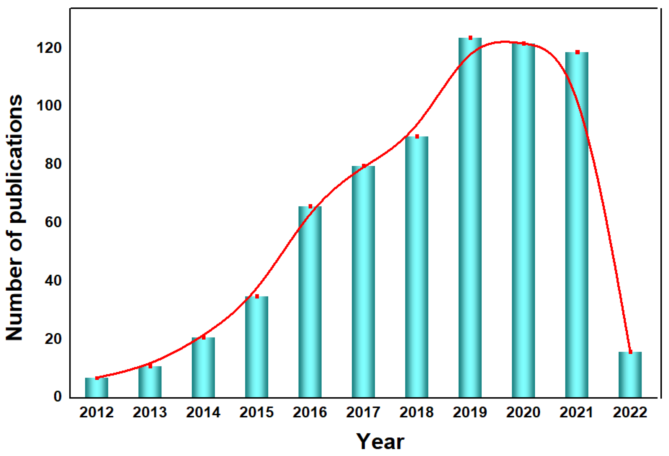
1. Introduction
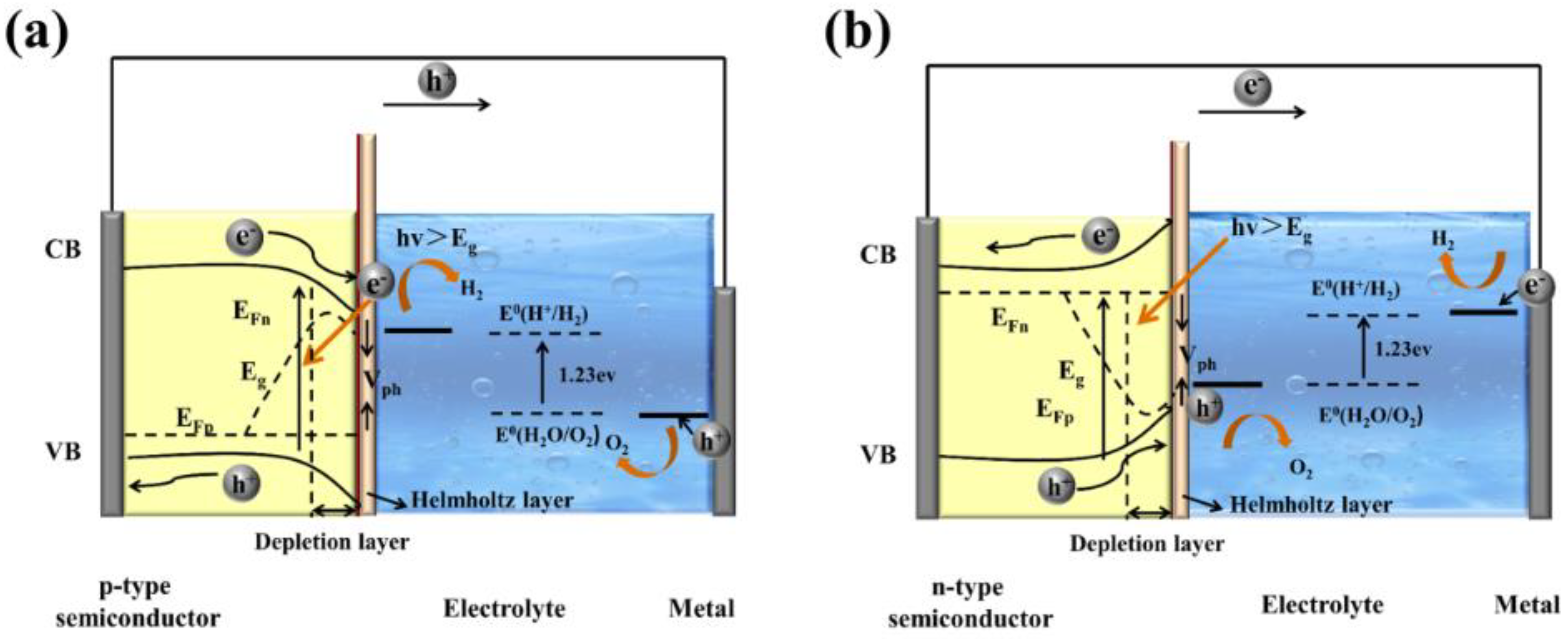
2. Water-Splitting Reaction Mechanisms
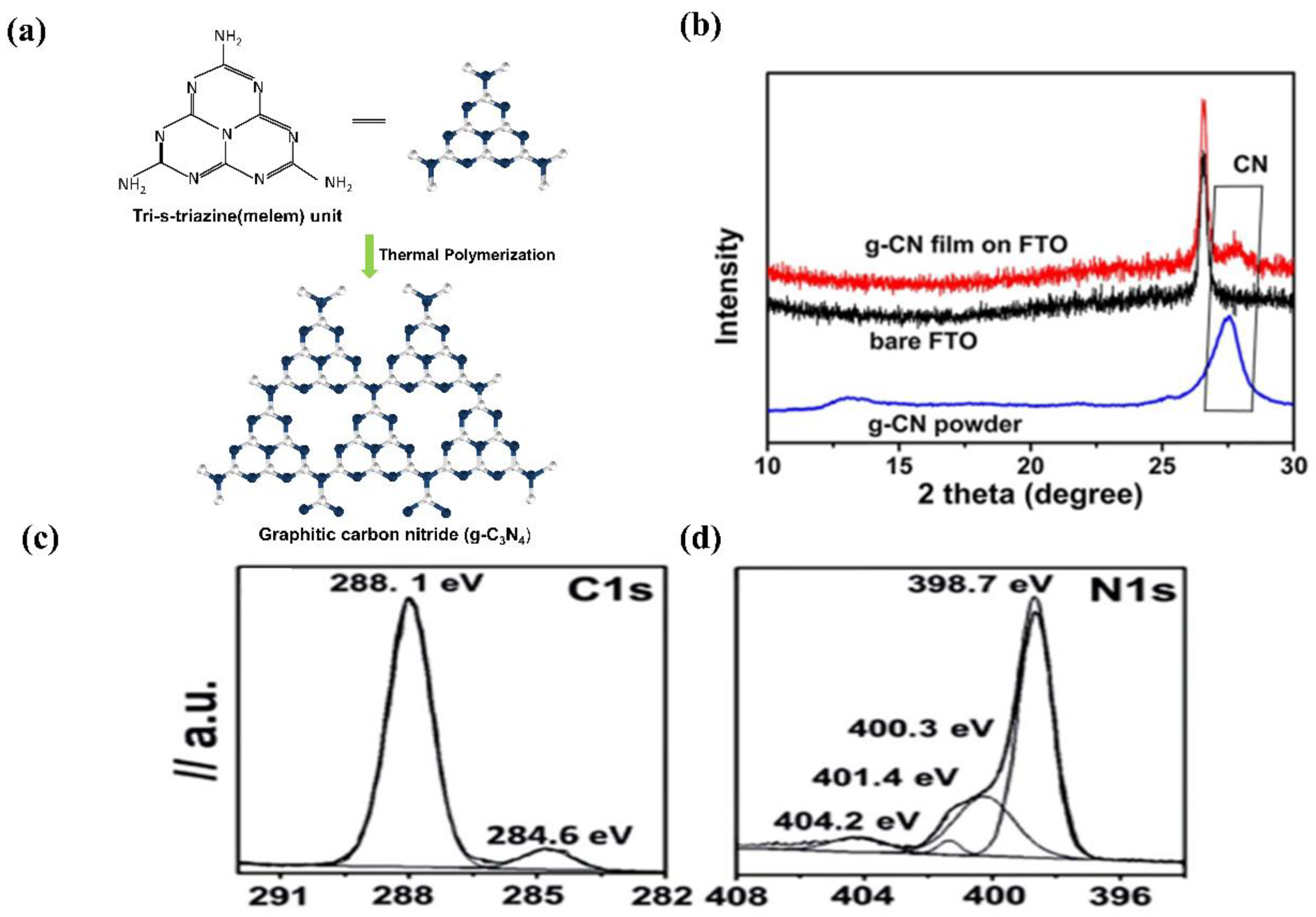
3. Electronic Structure of g−CN
4. g−CN Thin-Film Preparation Methods
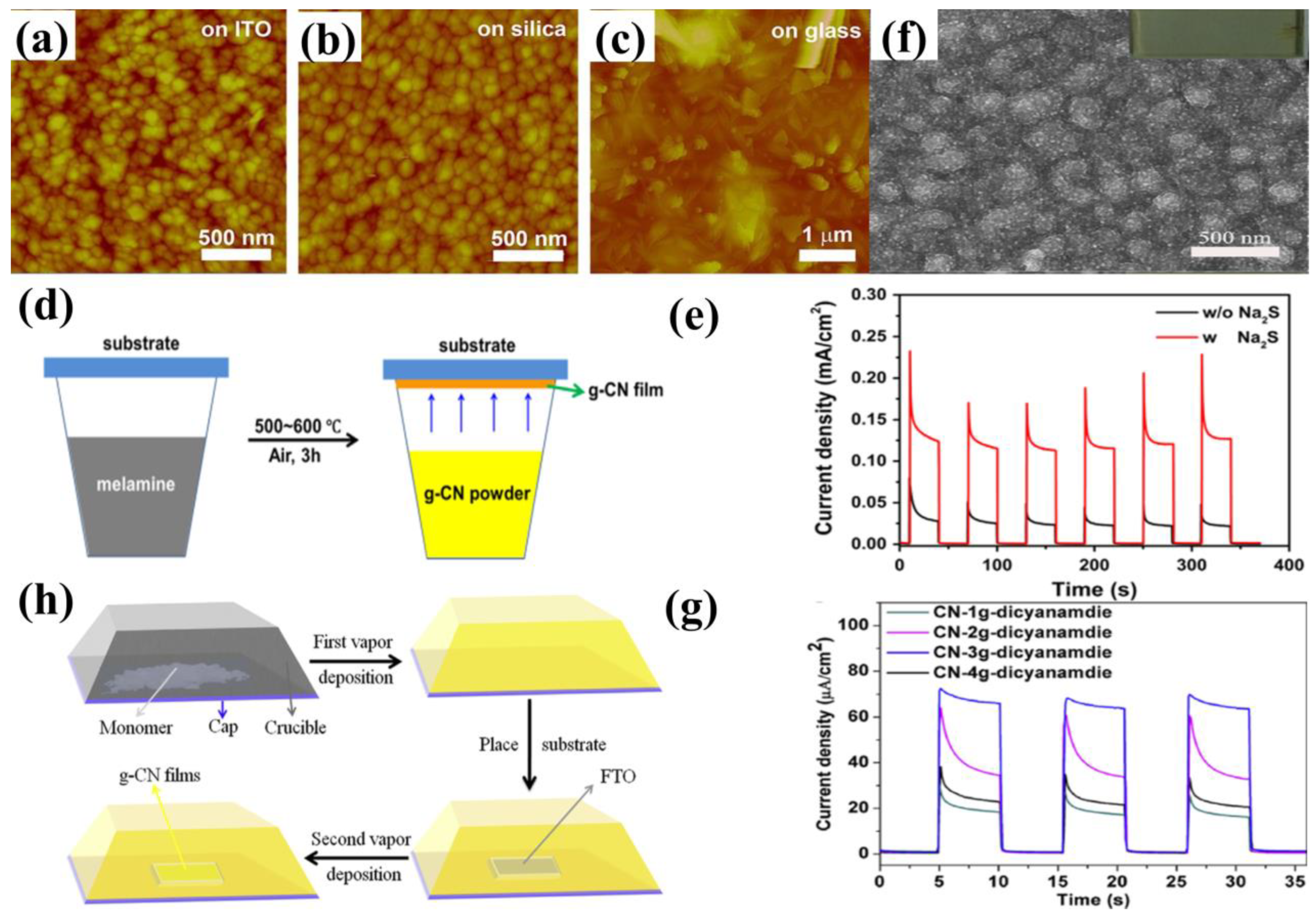
4.1. Thermal Vapor Condensation (TVC)
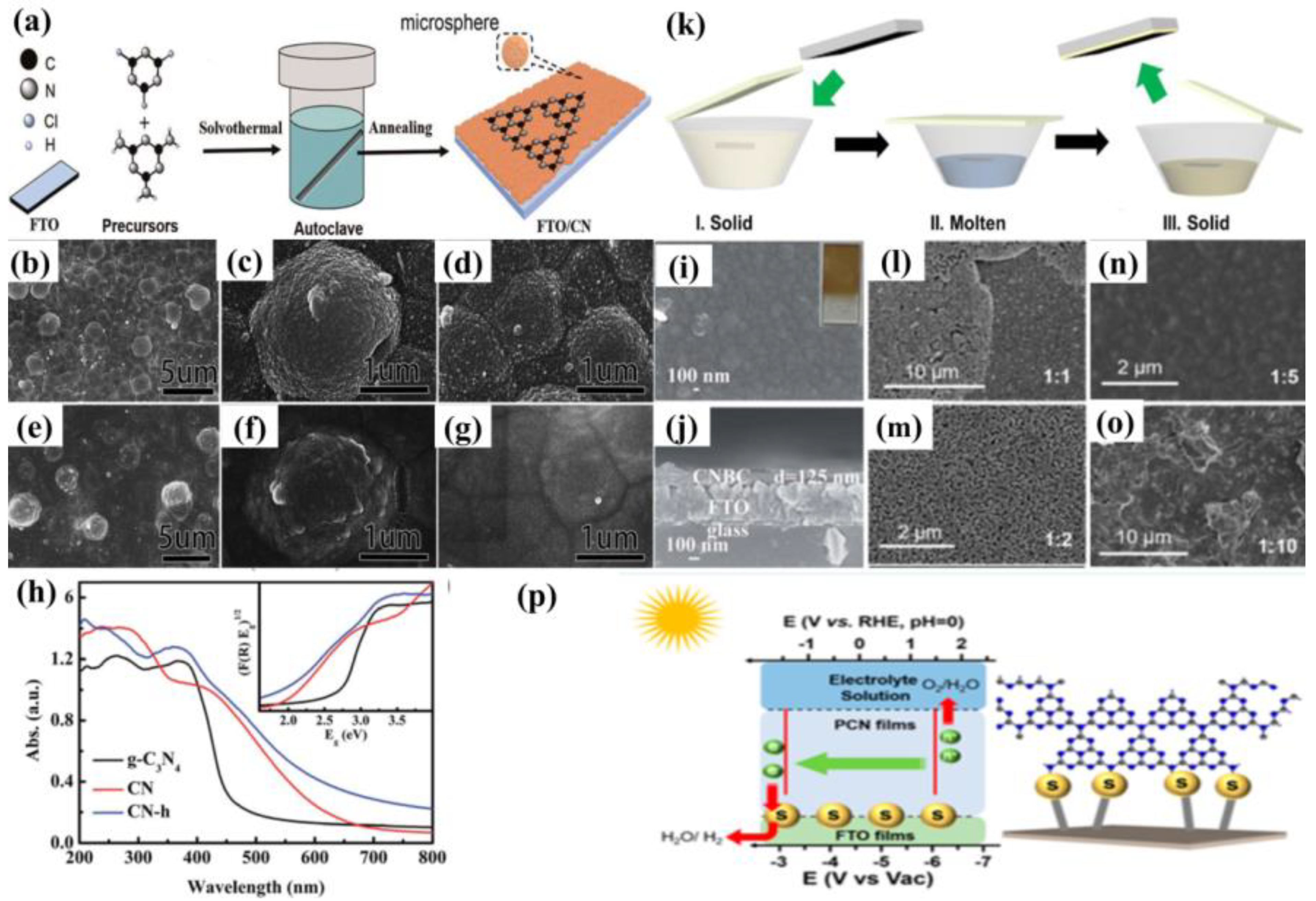
4.2. Solvothermal Route
4.3. Liquid-Mediated Growth
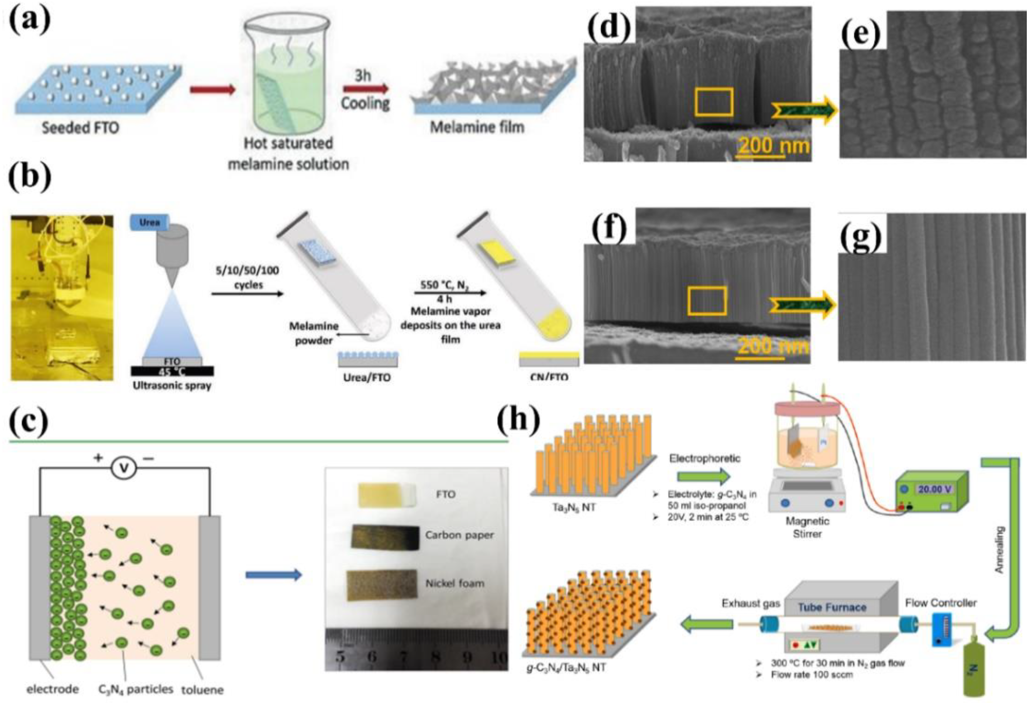
4.4. Seed Growth
4.5. Electrochemical Deposition

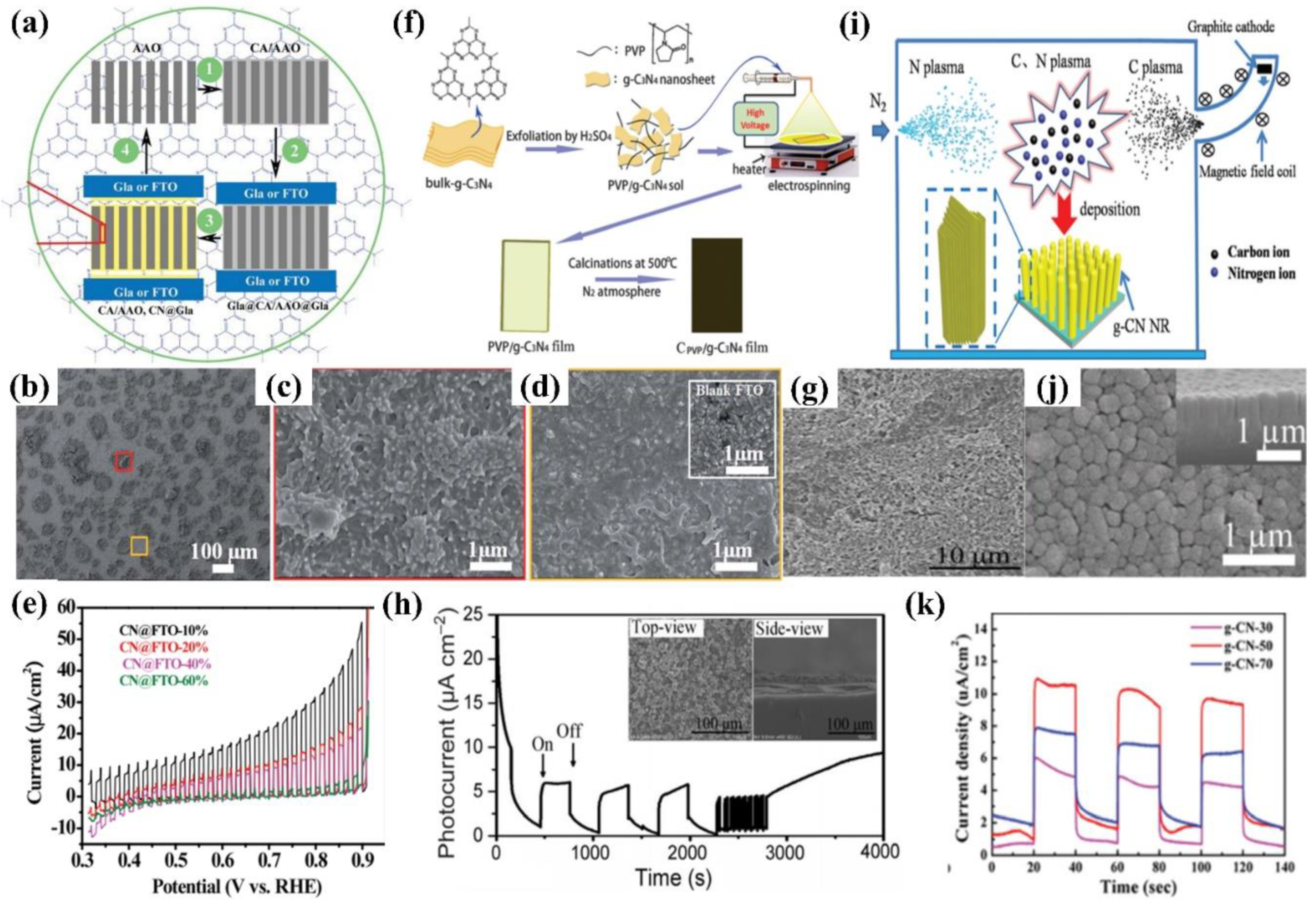
4.6. Disperse Coating
4.7. Other Deposition Methods
5. Functionalization of g−CN Photoelectrode
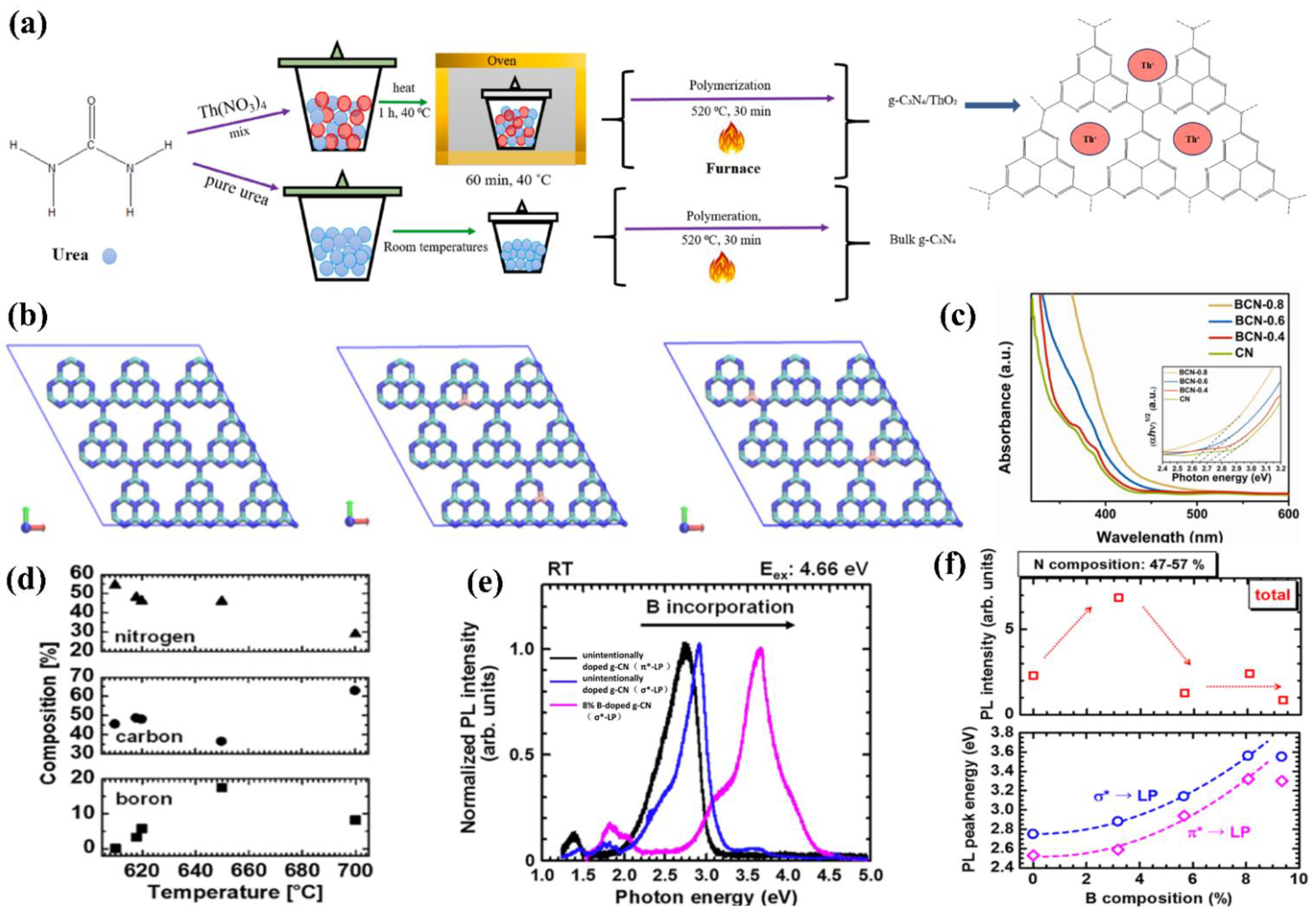
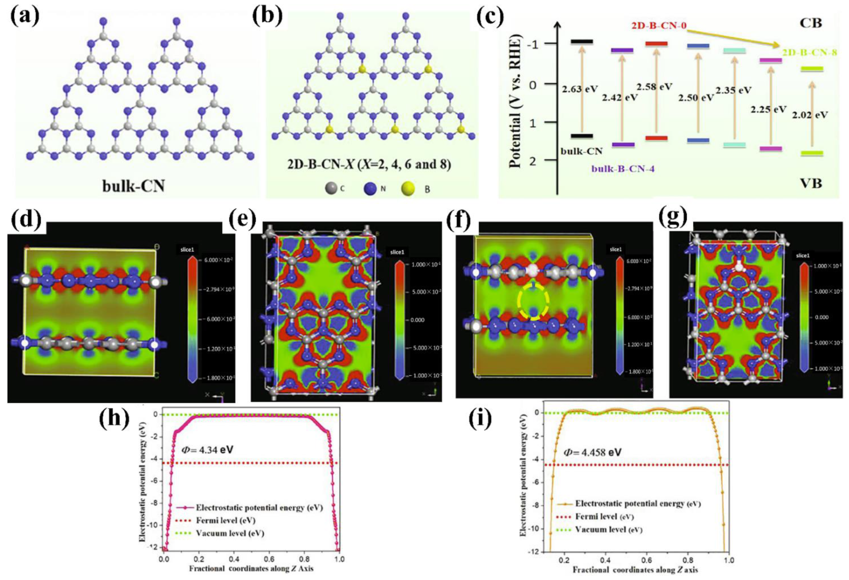
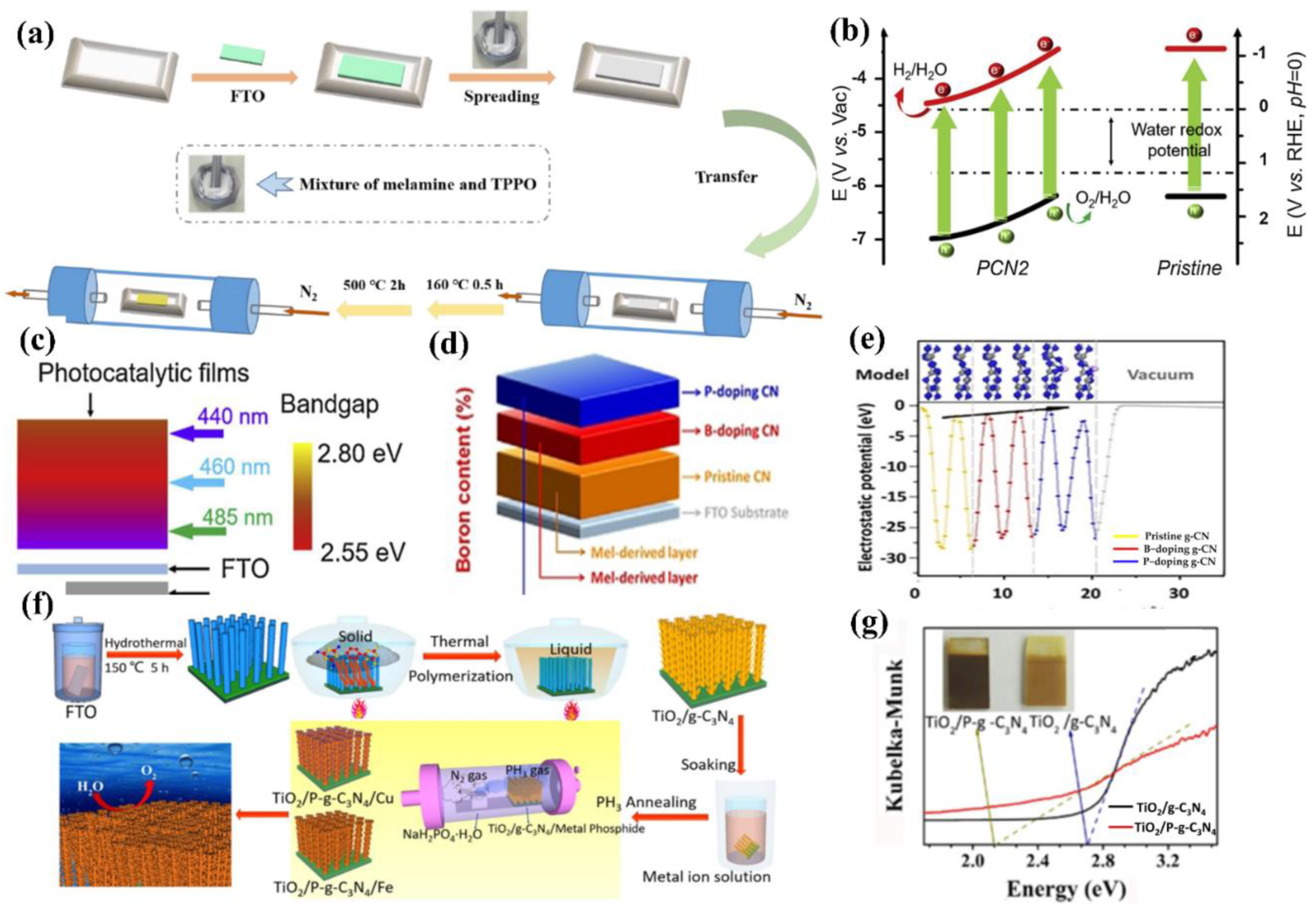
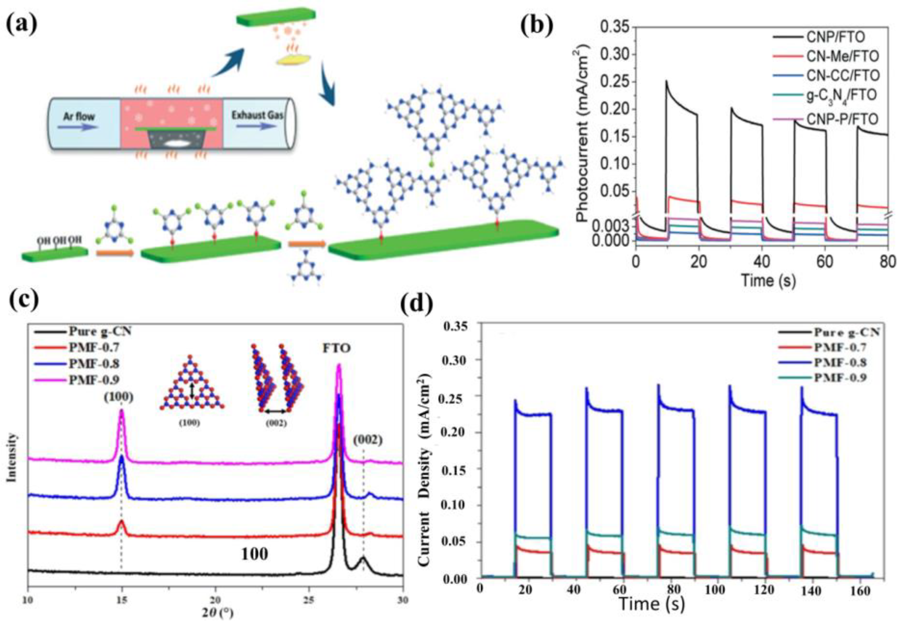
5.1. Heteroatoms Doping


5.2. Copolymerization of g−CN
5.3. Cocatalysts

6. Composite Films of g−CN as Highly Valid Photoelectrodes for PEC Application
6.1. Type II Heterojunctions
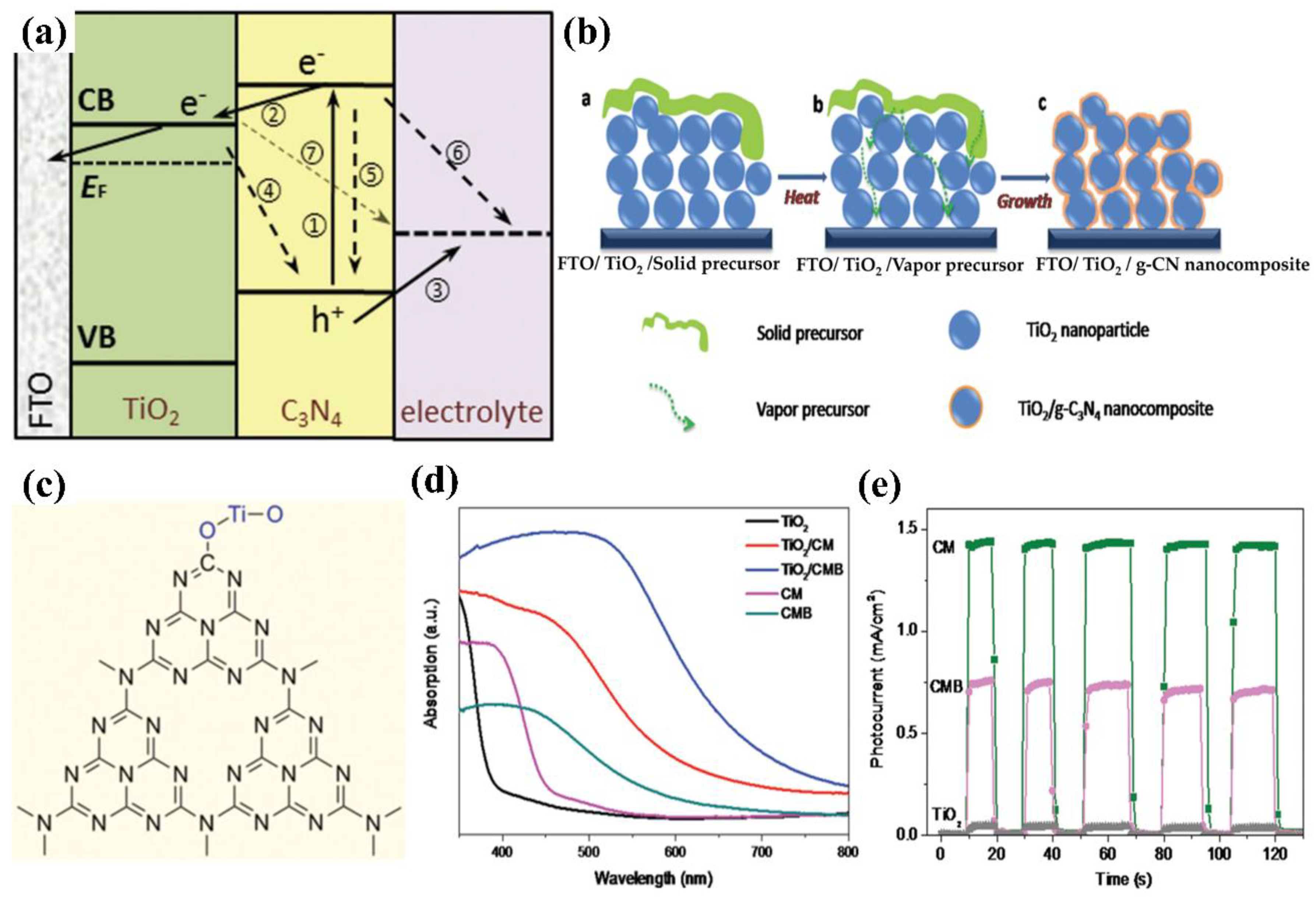
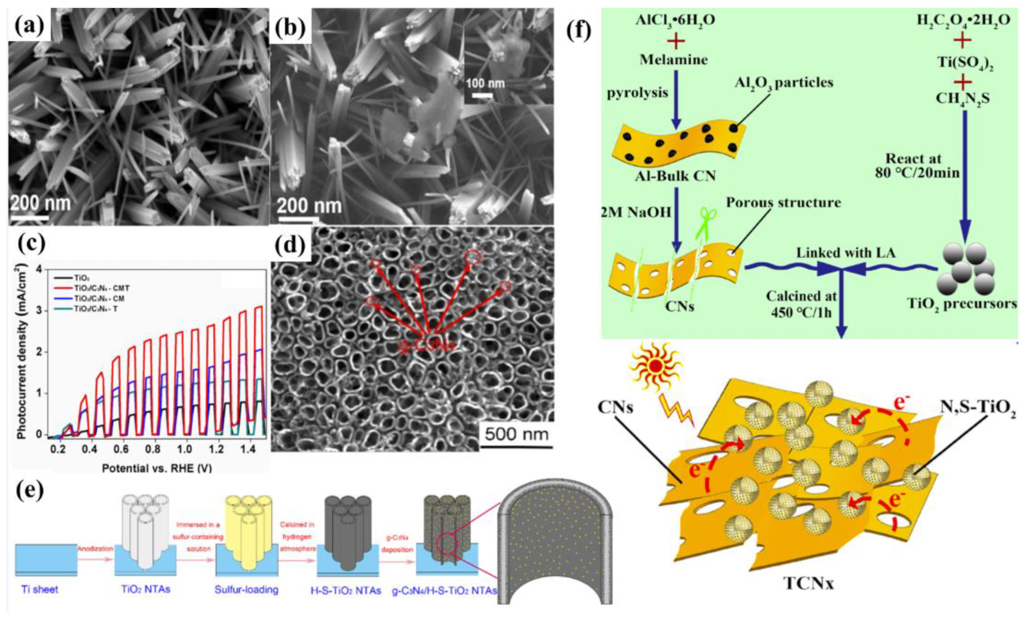
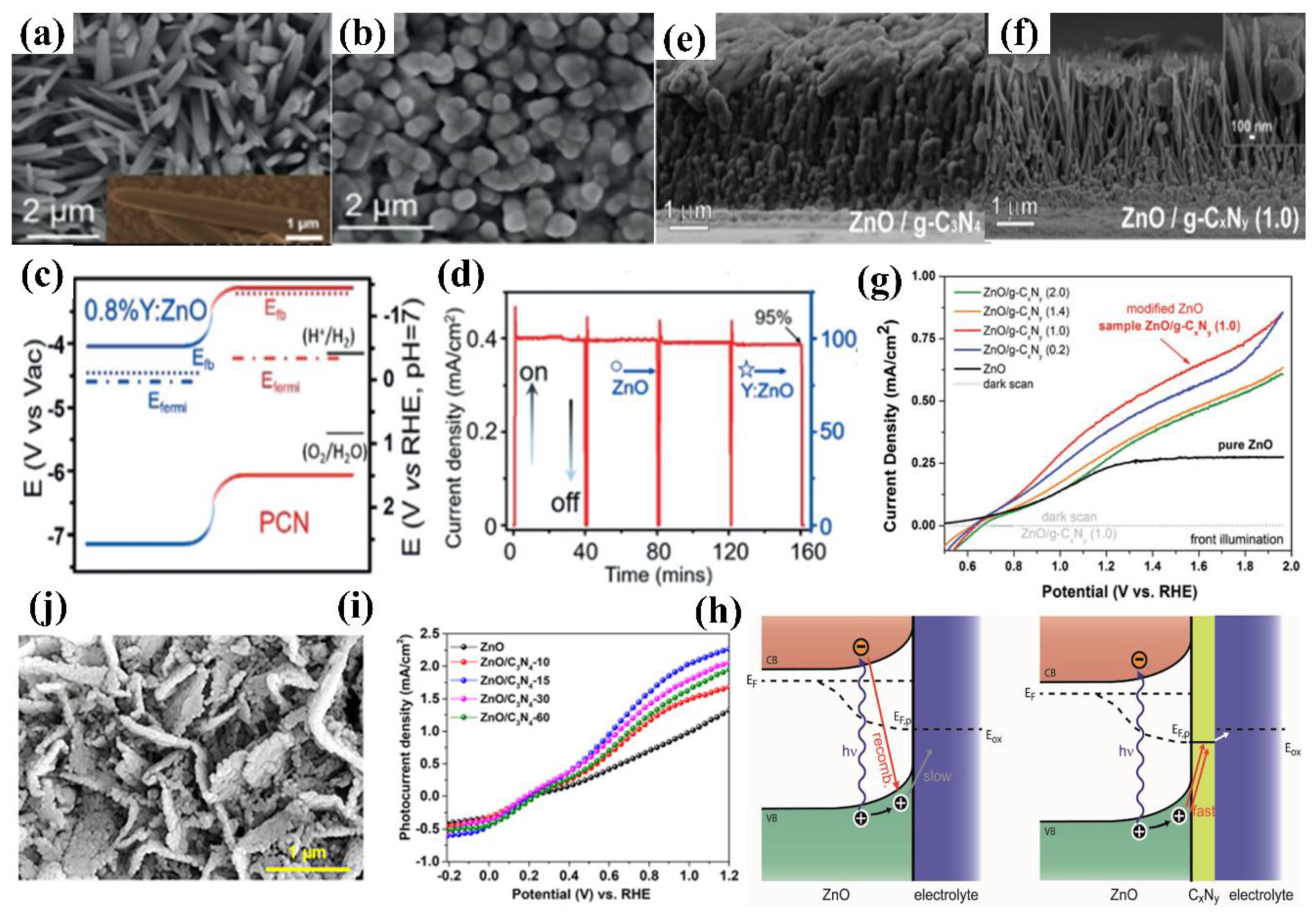
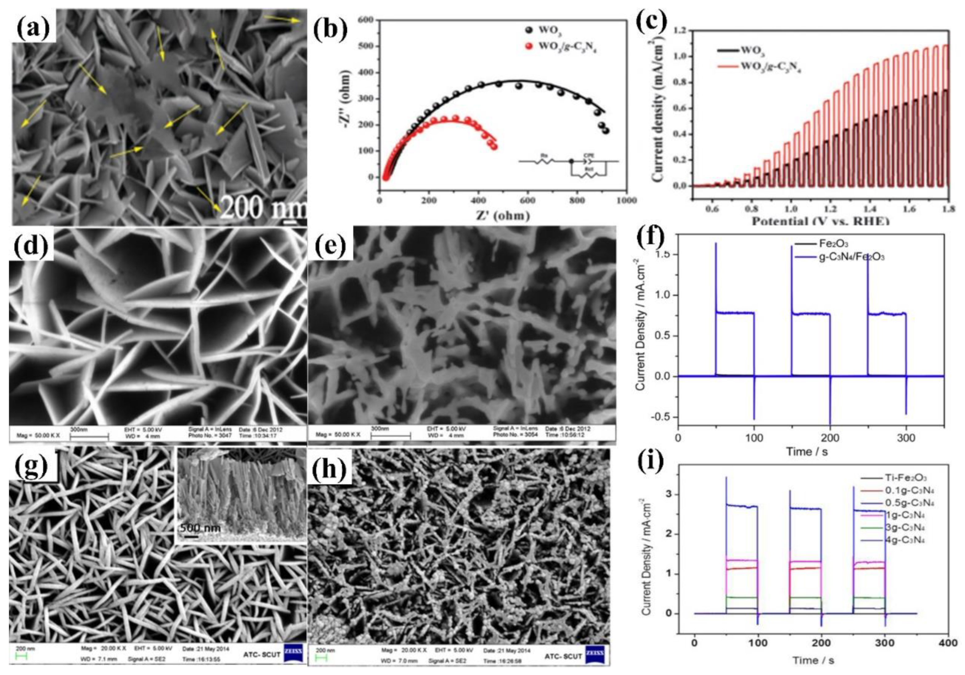
6.1.1. Metal Oxides/g−CN Hybrid Heterostructures Films

6.1.2. Metal Sulfides/g−CN Hybrid Heterostructures Films
6.1.3. Complex Compound/g−CN Hybrid Heterostructures Films

6.2. G−CN-based Z-Scheme Heterojunction Composite Films

6.3. Design and Construction of Multicomponent Heterojunctions

6.4. The Stability of the g−CN Photoelectrodes for PEC Applications
7. Conclusions, Perspective, and Outlook
- Improvement in the deposition methods:
- 2.
- Tuning the band gap of g−CN:
- 3.
- Improvement of photo-excited charge separation and suppression of the recombination of the carrier:
- 4.
- Enhancing the stability of g−CN:
Author Contributions
Funding
Data Availability Statement
Conflicts of Interest
References
- Huang, J.; Yu, H.; Dai, A.; Wei, Y.; Kang, L. Drylands face potential threat under 2 degrees Cglobal warming target. Nat. Clim. Chang. 2017, 7, 417–422. [Google Scholar] [CrossRef]
- Tokarska, K.B.; Gillett, N.P. Cumulative carbon emissions budgets consistent with 1.5 degrees C global warming. Nat. Clim. Chang. 2018, 8, 296–299. [Google Scholar] [CrossRef]
- Ong, W.-J.; Tan, L.-L.; Ng, Y.H.; Yong, S.-T.; Chai, S.-P. Graphitic Carbon Nitride (g-C3N4)-Based Photocatalysts for Artificial Photosynthesis and Environmental Remediation: Are We a Step Closer to Achieving Sustainability? Chem. Rev. 2016, 116, 7159–7329. [Google Scholar] [CrossRef]
- Du, M.; Cao, S.; Ye, X.; Ye, J. Recent Advances in the Fabrication of All-Solid-State Nanostructured TiO2-Based Z-Scheme Heterojunctions for Environmental Remediation. J. Nanosci. Nanotechnol. 2020, 20, 5861–5873. [Google Scholar] [CrossRef]
- Marchal, C.; Behr, M.; Vigneron, F.; Caps, V.; Keller, V. Au/TiO2 photocatalysts prepared by solid grinding for artificial solar-light water splitting. New J. Chem. 2016, 40, 4428–4435. [Google Scholar] [CrossRef]
- Fujishima, A.; Honda, K. Electrochemical photolysis of water at a semiconductor electrode. Nature 1972, 238, 37–38. [Google Scholar] [CrossRef]
- Malik, R.; Tomer, V.K. State-of-the-art review of morphological advancements in graphitic carbon nitride (g−CN) for sustainable hydrogen production. Renew. Sustain. Energy Rev. 2021, 135, 110235. [Google Scholar] [CrossRef]
- Kumar Singh, A.; Das, C.; Indra, A. Scope and prospect of transition metal-based cocatalysts for visible light-driven photocatalytic hydrogen evolution with graphitic carbon nitride. Coord. Chem. Rev. 2022, 465, 214516. [Google Scholar] [CrossRef]
- Zhang, W.; Xu, D.; Wang, F.; Chen, M. Element-doped graphitic carbon nitride: Confirmation of doped elements and applications. Nanoscale Adv. 2021, 3, 4370–4387. [Google Scholar] [CrossRef]
- Fang, Y.; Wang, X. Photocatalytic CO2 conversion by polymeric carbon nitrides. Chem. Commun. 2018, 54, 5674–5687. [Google Scholar] [CrossRef]
- Mansor, N.; Jorge, A.B.; Cora, F.; Gibbs, C.; Jervis, R.; McMillan, P.F.; Brett, D.J. Graphitic Carbon Nitride Supported Catalysts for Polymer Electrolyte Fuel Cells. J. Phys. Chem. C Nanomater. Interfaces 2014, 118, 6831–6838. [Google Scholar] [CrossRef]
- Sun, J.; Malishev, R.; Azoulay, A.; Tzadikov, J.; Volokh, M.; Jelinek, R.; Shalom, M. Carbon and Nitrogen Based Nanosheets as Fluorescent Probes with Tunable Emission. Small 2018, 14, e1800516. [Google Scholar] [CrossRef]
- Vinoth, S.; Pandikumar, A. Ni integrated S-gC3N4/BiOBr based Type-II heterojunction as a durable catalyst for photoelectrochemical water splitting. Renew. Energy 2021, 173, 507–519. [Google Scholar] [CrossRef]
- Zou, X.; Sun, Z.; Hu, Y.H. g-C3N4-based photoelectrodes for photoelectrochemical water splitting: A review. J. Mater. Chem. A 2020, 8, 21474–21502. [Google Scholar] [CrossRef]
- Heydari, M.; Azizi, N.; Mirjafari, Z.; Hashemi, M.M. Aluminum anchored on g-C3N4 as robust catalysts for Mannich reaction at ambient temperature. J. Mol. Struct. 2022, 1259, 132731. [Google Scholar] [CrossRef]
- Hayat, A.; Sohail, M.; Ali Shah Syed, J.; Al-Sehemi, A.G.; Mohammed, M.H.; Al-Ghamdi, A.A.; Muzibur Rahman, M. Recent Advancement of the Current Aspects of g-C3N4 for its Photocatalytic Applications in Sustainable Energy System. Chem. Rec. 2022, e202100310. [Google Scholar] [CrossRef]
- Volokh, M.; Peng, G.; Barrio, J.; Shalom, M. Carbon Nitride Materials for Water Splitting Photoelectrochemical Cells. Angew. Chem. Int. Ed. 2019, 58, 6138–6151. [Google Scholar] [CrossRef]
- Shang, T.; Chen, S.; Wei, Z.; Huang, D.; Yang, S. Construction of g-C3N4-Ferrocene Copolymers for Enhanced Visible-Light Photocatalytic Activity. Chem. Select. 2021, 6, 8114–8119. [Google Scholar]
- Gashi, A.; Parmentier, J.; Fioux, P.; Marsalek, R. Tuning the C/N Ratio of C-Rich Graphitic Carbon Nitride (g-C3N4) Materials by the Melamine/Carboxylic Acid Adduct Route. Chemistry 2022, 28, e202103605. [Google Scholar]
- Feng, C.; Wang, L.; Fu, S.; Fan, K.; Zhang, Y.; Bi, Y. Ultrathin FeFx nanolayers accelerating hole transfer for enhanced photoelectrochemical water oxidation. J. Mater. Chem. A 2018, 6, 19342–19346. [Google Scholar] [CrossRef]
- Zhong, M.; Hisatomi, T.; Sasaki, Y.; Suzuki, S.; Teshima, K.; Nakabayashi, M.; Domen, K. Highly Active GaN-Stabilized Ta3N5 Thin-Film Photoanode for Solar Water Oxidation. Angew. Chem. Int. Ed. 2017, 56, 4739–4743. [Google Scholar] [CrossRef] [PubMed]
- Liao, G.; Gong, Y.; Zhang, L.; Gao, H.; Yang, G.-J.; Fang, B. Semiconductor polymeric graphitic carbon nitride photocatalysts: The “holy grail” for the photocatalytic hydrogen evolution reaction under visible light. Energy Environ. Sci. 2019, 12, 2080–2147. [Google Scholar] [CrossRef]
- Samuel, E.; Joshi, B.; Kim, M.-W.; Swihart, M.T.; Yoon, S.S. Morphology engineering of photoelectrodes for efficient photoelectrochemical water splitting. Nano Energy 2020, 72, 104648. [Google Scholar] [CrossRef]
- Zhen, C.; Chen, R.; Wang, L.; Liu, G.; Cheng, H.-M. Tantalum (oxy)nitride based photoanodes for solar-driven water oxidation. J. Mater. Chem. A 2016, 4, 2783–2800. [Google Scholar] [CrossRef]
- Wang, S.; Liu, G.; Wang, L. Crystal Facet Engineering of Photoelectrodes for Photoelectrochemical Water Splitting. Chem Rev. 2019, 119, 5192–5247. [Google Scholar] [CrossRef]
- Murphy, A.; Barnes, P.; Randeniya, L.; Plumb, I.; Grey, I.; Horne, M.; Glasscock, J. Efficiency of solar water splitting using semiconductor electrodes. Int. J. Hydrogen Energy 2006, 31, 1999–2017. [Google Scholar] [CrossRef]
- Jiang, C.; Moniz, S.J.A.; Wang, A.; Zhang, T.; Tang, J. Photoelectrochemical devices for solar water splitting—Materials and challenges. Chem. Soc. Rev. 2017, 46, 4645–4660. [Google Scholar] [CrossRef]
- Liu, J.; Zhao, X.; Jing, P.; Shi, W.; Chen, P. A Metal-Organic-Framework-Derived g-C3N4/alpha-Fe2O3 Hybrid for Enhanced Visible-Light-Driven Photocatalytic Hydrogen Evolution. Chem. Eur. J. 2019, 25, 2330–2336. [Google Scholar]
- Cheng, C.; Zhang, W.; Chen, X.; Peng, S.; Li, Y. Strategies for improving photoelectrochemical water splitting performance of Si-based electrodes. Energy Sci. Eng. 2022, 10, 1526–1543. [Google Scholar] [CrossRef]
- Pastika, J.; Oliveira, F.M.; Mazanek, V.; Sofer, Z.; Gusmao, R. Synthesis of Magnesium Phosphorous Trichalcogenides and Applications in Photoelectrochemical Water Splitting. Small 2022, 18, 2200355. [Google Scholar] [CrossRef]
- Wang, X.; Maeda, K.; Thomas, A.; Takanabe, K.; Xin, G.; Carlsson, J.M.; Antonietti, M. A metal-free polymeric photocatalyst for hydrogen production from water under visible light. Nat. Mater. 2009, 8, 76–80. [Google Scholar] [CrossRef] [PubMed]
- Wang, Y.; Wang, X.; Antonietti, M. Polymeric Graphitic Carbon Nitride as a Heterogeneous Organocatalyst: From Photochemistry to Multipurpose Catalysis to Sustainable Chemistry. Angew. Chem. Int. Ed. 2012, 51, 68–89. [Google Scholar] [CrossRef] [PubMed]
- Zheng, Y.; Lin, L.; Wang, B.; Wang, X. Graphitic Carbon Nitride Polymers toward Sustainable Photoredox Catalysis. Angew. Chem. Int. Ed. 2015, 54, 12868–12884. [Google Scholar] [CrossRef] [PubMed]
- Bian, J.; Li, J.; Kalytchuk, S.; Wang, Y.; Li, Q.; Lau, T.C.; Zhang, R.-Q. Efficient Emission Facilitated by Multiple Energy Level Transitions in Uniform Graphitic Carbon Nitride Films Deposited by Thermal Vapor Condensation. Chemphyschem 2015, 16, 954–959. [Google Scholar] [CrossRef]
- Safaei, J.; Ullah, H.; Mohamed, N.A.; Noh, M.F.M.; Soh, M.F.; Tahir, A.A.; Teridi, M.A.M. Enhanced photoelectrochemical performance of Z-scheme g-C3N4/BiVO4 photocatalyst. Appl. Catal. B. 2018, 234, 296–310. [Google Scholar] [CrossRef]
- Zhang, G.; Zhang, J.; Zhang, M.; Wang, X. Polycondensation of thiourea into carbon nitride semiconductors as visible light photocatalysts. J. Mater. Chem. 2012, 22, 8083–8091. [Google Scholar] [CrossRef]
- Ehrmaier, J.; Domcke, W.; Opalka, D. Mechanism of Photocatalytic Water Oxidation by Graphitic Carbon Nitride. J. Phys. Chem. Lett. 2018, 9, 4695–4699. [Google Scholar] [CrossRef]
- Ehrmaier, J.; Karsili, T.N.V.; Sobolewski, A.L.; Domcke, W. Mechanism of Photocatalytic Water Splitting with Graphitic Carbon Nitride: Photochemistry of the Heptazine-Water Complex. J. Phys. Chem. A. 2017, 121, 4754–4764. [Google Scholar] [CrossRef]
- Ehrmaier, J.; Janicki, M.J.; Sobolewski, A.L.; Domcke, W. Mechanism of photocatalytic water splitting with triazine-based carbon nitrides: Insights from ab initio calculations for the triazine-water complex. Phys. Chem. Chem. Phys. 2018, 20, 14420–14430. [Google Scholar] [CrossRef]
- Dong, F.; Zhao, Z.; Xiong, T.; Ni, Z.; Zhang, W.; Sun, Y.; Ho, W.-K. In Situ Construction of g-C3N4/g-C3N4 Metal-Free Heterojunction for Enhanced Visible-Light Photocatalysis. ACS Appl. Mater. Interfaces 2013, 5, 11392–11401. [Google Scholar] [CrossRef]
- Zhang, J.; Chen, X.; Takanabe, K.; Maeda, K.; Domen, K.; Epping, J.D.; Wang, X. Synthesis of a Carbon Nitride Structure for Visible-Light Catalysis by Copolymerization. Angew. Chem. Int. Ed. 2010, 49, 441–444. [Google Scholar] [CrossRef] [PubMed]
- Zhang, J.; Zhang, M.; Lin, L.; Wang, X. Sol Processing of Conjugated Carbon Nitride Powders for Thin-Film Fabrication. Angew. Chem. Int. Ed. 2015, 54, 6297–6301. [Google Scholar] [CrossRef] [PubMed]
- Bi, L.; Xu, D.; Zhang, L.; Lin, Y.; Wang, D.; Xie, T. Metal Ni-loaded g-C3N4 for enhanced photocatalytic H2 evolution activity: The change in surface band bending. Phys. Chem. Chem. Phys. 2015, 17, 29899–29905. [Google Scholar] [CrossRef]
- Wang, H.; Zhang, X.; Xie, J.; Zhang, J.; Ma, P.; Pan, B.; Xie, Y. Structural distortion in graphitic-C3N4 realizing an efficient photoreactivity. Nanoscale 2015, 7, 5152–5156. [Google Scholar] [CrossRef] [PubMed]
- Li, H.; Yu, H.; Quan, X.; Chen, S.; Zhang, Y. Uncovering the Key Role of the Fermi Level of the Electron Mediator in a Z-Scheme Photocatalyst by Detecting the Charge Transfer Process of WO3-metal-g-C3N4 (Metal = Cu, Ag, Au). ACS Appl. Mater. Interfaces 2016, 8, 2111–2119. [Google Scholar] [CrossRef] [PubMed]
- Kang, Y.; Yang, Y.; Yin, L.-C.; Kang, X.; Liu, G.; Cheng, H.-M. An Amorphous Carbon Nitride Photocatalyst with Greatly Extended Visible-Light-Responsive Range for Photocatalytic Hydrogen Generation. Adv. Mater. 2015, 27, 4572–4577. [Google Scholar] [CrossRef]
- Ragupathi, V.; Panigrahi, P.; Subramaniam, N.G. Bandgap engineering in graphitic carbon nitride: Effect of precursors. Optik 2020, 202, 163601. [Google Scholar] [CrossRef]
- Bian, J.; Li, Q.; Huang, C.; Li, J.; Guo, Y.; Zaw, M.; Zhang, R.-Q. Thermal vapor condensation of uniform graphitic carbon nitride films with remarkable photocurrent density for photoelectrochemical applications. Nano Energy 2015, 15, 353–361. [Google Scholar] [CrossRef]
- Lv, X.; Cao, M.; Shi, W.; Wang, M.; Shen, Y. A new strategy of preparing uniform graphitic carbon nitride films for photoelectrochemical application. Carbon 2017, 117, 343–350. [Google Scholar] [CrossRef]
- Bian, J.; Xi, L.; Li, J.; Xiong, Z.; Huang, C.; Lange, K.M.; Zhang, R.-Q. C=C pi Bond Modified Graphitic Carbon Nitride Films for Enhanced Photoelectrochemical Cell Performance. Chem. Asian J. 2017, 12, 1005–1012. [Google Scholar] [CrossRef]
- Lu, X.; Liu, Z.; Li, J.; Zhang, J.; Guo, Z. Novel framework g-C3N4 film as efficient photoanode for photoelectrochemical water splitting. Appl. Catal. B. 2017, 209, 657–662. [Google Scholar] [CrossRef]
- Mohamed, N.A.; Safaei, J.; Ismail, A.F.; Jailani, M.F.A.M.; Khalid, M.N.; Noh, M.F.M.; Teridi, M.A.M. The influences of post-annealing temperatures on fabrication graphitic carbon nitride, (g-C3N4) thin film. Appl. Surf. Sci. 2019, 489, 92–100. [Google Scholar] [CrossRef]
- Bian, J.; Xi, L.; Huang, C.; Lange, K.M.; Zhang, R.-Q.; Shalom, M. Efficiency Enhancement of Carbon Nitride Photoelectrochemical Cells via Tailored Monomers Design. Adv. Energy Mater. 2016, 6, 1600263. [Google Scholar] [CrossRef]
- Yan, S.C.; Li, Z.S.; Zou, Z.G. Photodegradation Performance of g-C3N4 Fabricated by Directly Heating Melamine. Langmuir 2009, 25, 10397–10401. [Google Scholar] [CrossRef] [PubMed]
- Fujita, S.; Habuchi, H.; Takagi, S.; Takikawa, H. Optical properties of graphitic carbon nitride films prepared by evaporation. Diamond Relat. Mater. 2016, 65, 83–86. [Google Scholar] [CrossRef]
- Urakami, N.; Kosaka, M.; Hashimoto, Y. Thermal chemical vapor deposition and luminescence property of graphitic carbon nitride film for carbon-based semiconductor systems. Jpn. J. Appl. Phys. 2019, 58, 010907. [Google Scholar] [CrossRef]
- Xie, X.; Fan, X.; Huang, X.; Wang, T.; He, J. In situ growth of graphitic carbon nitride films on transparent conducting substrates via a solvothermal route for photoelectrochemical performance. RSC Adv. 2016, 6, 9916–9922. [Google Scholar] [CrossRef]
- Gu, Q.; Gong, X.; Jia, Q.; Liu, J.; Gao, Z.; Wang, X.; Xue, C. Compact carbon nitride based copolymer films with controllable thickness for photoelectrochemical water splitting. J. Mater. Chem. A 2017, 5, 19062–19071. [Google Scholar] [CrossRef]
- Xu, J.; Brenner, T.J.K.; Chabanne, L.; Neher, D.; Antonietti, M.; Shalom, M. Liquid-Based Growth of Polymeric Carbon Nitride Layers and Their Use in a Mesostructured Polymer Solar Cell with V-oc Exceeding 1 V. J. Am. Chem. Soc. 2014, 136, 13486–13489. [Google Scholar] [CrossRef]
- Jun, Y.-S.; Lee, E.Z.; Wang, X.; Hong, W.H.; Stucky, G.D.; Thomas, A. From Melamine-Cyanuric Acid Supramolecular Aggregates to Carbon Nitride Hollow Spheres. Adv. Funct. Mater. 2013, 23, 3661–3667. [Google Scholar] [CrossRef]
- Shalom, M.; Gimenez, S.; Schipper, F.; Herraiz-Cardona, I.; Bisquert, J.; Antonietti, M. Controlled Carbon Nitride Growth on Surfaces for Hydrogen Evolution Electrodes. Angew. Chem. Int. Ed. 2014, 53, 3654–3658. [Google Scholar] [CrossRef] [PubMed]
- Xu, J.; Cao, S.; Brenner, T.; Yang, X.; Yu, J.; Antonietti, M.; Shalom, M. Supramolecular Chemistry in Molten Sulfur: Preorganization Effects Leading to Marked Enhancement of Carbon Nitride Photoelectrochemistry. Adv. Funct. Mater. 2015, 25, 6265–6271. [Google Scholar] [CrossRef]
- Shalom, M.; Inal, S.; Fettkenhauer, C.; Neher, D.; Antonietti, M. Improving Carbon Nitride Photocatalysis by Supramolecular Preorganization of Monomers. J. Am. Chem. Soc. 2013, 135, 7118–7121. [Google Scholar] [CrossRef] [PubMed]
- Fang, Y.; Li, X.; Wang, X. Synthesis of Polymeric Carbon Nitride Films with Adhesive Interfaces for Solar Water Splitting Devices. ACS Catal. 2018, 8, 8774–8780. [Google Scholar] [CrossRef]
- Zhang, W.; Albero, J.; Xi, L.; Lange, K.M.; Garcia, H.; Wang, X.; Shalom, M. One-Pot Synthesis of Nickel-Modified Carbon Nitride Layers Toward Efficient Photoelectrochemical Cells. ACS Appl. Mater. Interfaces 2017, 9, 32667–32677. [Google Scholar] [CrossRef] [PubMed]
- Peng, G.; Albero, J.; Garcia, H.; Shalom, M. A Water-Splitting Carbon Nitride Photoelectrochemical Cell with Efficient Charge Separation and Remarkably Low Onset Potential. Angew. Chem. Int. Ed. 2018, 57, 15807–15811. [Google Scholar] [CrossRef]
- Peng, G.; Qin, J.; Volokh, M.; Shalom, M. Freestanding Hierarchical Carbon Nitride/Carbon-Paper Electrode as a Photoelectrocatalyst for Water Splitting and Dye Degradation. ACS Appl. Mater. Interfaces 2019, 11, 29139–29146. [Google Scholar] [CrossRef]
- Tashakory, A.; Karjule, N.; Abisdris, L.; Volokh, M.; Shalom, M. Mediated Growth of Carbon Nitride Films via Spray-Coated Seeding Layers for Photoelectrochemical Applications. Adv. Sustain. Syst. 2021, 5, 2100005. [Google Scholar] [CrossRef]
- Kang, D.; Kim, T.W.; Kubota, S.R.; Cardiel, A.C.; Cha, H.G.; Choi, K.-S. Electrochemical Synthesis of Photoelectrodes and Catalysts for Use in Solar Water Splitting. Chem. Rev. 2015, 115, 12839–12887. [Google Scholar] [CrossRef]
- Li, C.; Cao, C.B.; Zhu, H.S. Graphitic carbon nitride thin films deposited by electrodeposition. Mater. Lett. 2004, 58, 1903–1906. [Google Scholar] [CrossRef]
- Xu, J.; Shalom, M. Electrophoretic Deposition of Carbon Nitride Layers for Photoelectrochemical Applications. ACS Appl. Mater. Interfaces 2016, 8, 13058–13063. [Google Scholar] [CrossRef] [PubMed]
- Das, P.K.; Poonchi Sivasankaran, R.; Arunachalam, M.; Subhash, K.R.; Ha, J.-S.; Ahn, K.-S.; Kang, S.H. Highly efficient and stable g-C3N4 decorated Ta3N5 nanotube on n-Si substrate for solar water oxidation. Appl. Surf. Sci. 2021, 565, 150456. [Google Scholar] [CrossRef]
- Li, K.; Zeng, X.; Gao, S.; Ma, L.; Wang, Q.; Xu, H.; Lu, J. Ultrasonic-assisted pyrolyzation fabrication of reduced SnO2-x/g-C3N4 heterojunctions: Enhance photoelectrochemical and photocatalytic activity under visible LED light irradiation. Nano Res. 2016, 9, 1969–1982. [Google Scholar] [CrossRef]
- Kokane, S.B.; Sasikala, R.; Phase, D.M.; Sartale, S.D. In2S3 nanoparticles dispersed on g-C3N4 nanosheets: Role of heterojunctions in photoinduced charge transfer and photoelectrochemical and photocatalytic performance. J. Mater. Sci. 2017, 52, 7077–7090. [Google Scholar] [CrossRef]
- Zhang, Y.; Thomas, A.; Antonietti, M.; Wang, X. Activation of Carbon Nitride Solids by Protonation: Morphology Changes, Enhanced Ionic Conductivity, and Photoconduction Experiments. J. Am. Chem. Soc. 2009, 131, 50–51. [Google Scholar] [CrossRef]
- Bai, X.; Wang, L.; Zong, R.; Zhu, Y. Photocatalytic Activity Enhanced via g-C3N4 Nanoplates to Nanorods. J. Phys. Chem. C 2013, 117, 9952–9961. [Google Scholar] [CrossRef]
- Wang, Y.; Zhao, X.; Tian, Y.; Wang, Y.; Jan, A.K.; Chen, Y. Facile Electrospinning Synthesis of Carbonized Polyvinylpyrrolidone (PVP)/g-C3N4 Hybrid Films for Photoelectrochemical Applications. Chem. Eur. J. 2017, 23, 419–426. [Google Scholar] [CrossRef]
- Tong, J.; Zhang, L.; Li, F.; Wang, K.; Han, L.; Cao, S. Rapid and high-yield production of g-C3N4 nanosheets via chemical exfoliation for photocatalytic H-2 evolution. RSC Adv. 2015, 5, 88149–88153. [Google Scholar] [CrossRef]
- Han, Q.; Wang, B.; Gao, J.; Cheng, Z.; Zhao, Y.; Zhang, Z.; Qu, L. Atomically Thin Mesoporous Nanomesh of Graphitic C3N4 for High-Efficiency Photocatalytic Hydrogen Evolution. ACS Nano 2016, 10, 2745–2751. [Google Scholar] [CrossRef]
- Lin, Q.; Li, L.; Liang, S.; Liu, M.; Bi, J.; Wu, L. Efficient synthesis of monolayer carbon nitride 2D nanosheet with tunable concentration and enhanced visible-light photocatalytic activities. Appl. Catal. B. 2015, 163, 135–142. [Google Scholar] [CrossRef]
- Qi, L.-Y.; Zhang, Y.-W.; Zuo, Z.-C.; Xin, Y.-L.; Yang, C.-K.; Wu, B.; Zhou, H.-H. In situ quantization of ferroferric oxide embedded in 3D microcarbon for ultrahigh performance sodium-ion batteries. J. Mater. Chem. A 2016, 4, 8822–8829. [Google Scholar] [CrossRef]
- Wang, X.; Blechert, S.; Antonietti, M. Polymeric Graphitic Carbon Nitride for Heterogeneous Photocatalysis. ACS Catal. 2012, 2, 1596–1606. [Google Scholar] [CrossRef]
- Safaei, J.; Mohamed, N.A.; Noh, M.F.M.; Soh, M.F.; Ludin, N.A.; Ibrahim, M.A.; Teridi, M.A.M. Graphitic carbon nitride (g-C3N4) electrodes for energy conversion and storage: A review on photoelectrochemical water splitting, solar cells and supercapacitors. J. Mater. Chem. A 2018, 6, 22346–22380. [Google Scholar] [CrossRef]
- Xu, J.; Zhang, L.; Shi, R.; Zhu, Y. Chemical exfoliation of graphitic carbon nitride for efficient heterogeneous photocatalysis. J. Mater. Chem. A 2013, 1, 14766–14772. [Google Scholar] [CrossRef]
- Khezami, L.; Ben Aissa, M.A.; Modwi, A.; Ismail, M.; Guesmi, A.; Algethami, F.K.; Nguyen-Tri, P. Harmonizing the photocatalytic activity of g-C3N4 nanosheets by ZrO2 stuffing: From fabrication to experimental study for the wastewater treatment. Biochem. Eng. J. 2022, 182, 108411. [Google Scholar] [CrossRef]
- Safaei, J.; Mohamed, N.A.; Noh, M.F.M.; Soh, M.F.; Riza, M.A.; Mustakim, N.S.M.; Teridi, M.A.M. Facile fabrication of graphitic carbon nitride, (g-C3N4) thin film. J. Alloys Compd. 2018, 769, 130–135. [Google Scholar] [CrossRef]
- Mohamed, N.A.; Safaei, J.; Ismail, A.F.; Noh, M.F.M.; Arzaee, N.A.; Mansor, N.N.; Teridi, M.A.M. Fabrication of exfoliated graphitic carbon nitride, (g-C3N4) thin film by methanolic dispersion. J. Alloys Compd. 2020, 818, 152916. [Google Scholar] [CrossRef]
- Zheng, D.; Huang, C.; Wang, X. Post-annealing reinforced hollow carbon nitride nanospheres for hydrogen photosynthesis. Nanoscale 2015, 7, 465–470. [Google Scholar] [CrossRef]
- Peng, G.; Xing, L.; Barrio, J.; Volokh, M.; Shalom, M. A General Synthesis of Porous Carbon Nitride Films with Tunable Surface Area and Photophysical Properties. Angew. Chem. Int. Ed. 2018, 57, 1186–1192. [Google Scholar] [CrossRef]
- Liu, J.; Wang, H.; Chen, Z.P.; Moehwald, H.; Fiechter, S.; van de Krol, R.; Antonietti, M. Microcontact-Printing-Assisted Access of Graphitic Carbon Nitride Films with Favorable Textures toward Photoelectrochemical Application. Adv. Mater. 2015, 27, 712–718. [Google Scholar] [CrossRef]
- Miao, H.; Zhang, G.; Hu, X.; Mu, J.; Han, T.; Fan, J.; Hou, X. A novel strategy to prepare 2D g-C3N4 nanosheets and their photoelectrochemical properties. J. Alloys Compd. 2017, 690, 669–676. [Google Scholar] [CrossRef]
- Zhang, X.; Xie, X.; Wang, H.; Zhang, J.; Pan, B.; Xie, Y. Enhanced Photoresponsive Ultrathin Graphitic-Phase C3N4 Nanosheets for Bioimaging. J. Am. Chem. Soc. 2013, 135, 18–21. [Google Scholar] [CrossRef] [PubMed]
- Wang, R.; Liu, H.; Fan, Z.; Li, L.; Cai, Y.; Xu, G.; Zou, Z. Unconventional gas-based bottom-up, meter-area-scale fabrication of hydrogen-bond free g−CN nanorod arrays and coupling layers with TiO2 toward high-efficiency photoelectrochemical performance. Nanoscale 2018, 10, 3342–3349. [Google Scholar] [CrossRef] [PubMed]
- Ladva, S.A.; Travis, W.; Quesada-Cabrera, R.; Rosillo-Lopez, M.; Afandi, A.; Li, Y.; Palgrave, R.G. Nanoscale, conformal films of graphitic carbon nitride deposited at room temperature: A method for construction of heterojunction devices. Nanoscale 2017, 9, 16586–16590. [Google Scholar] [CrossRef]
- Tejasvi, R.; Basu, S. Formation of C3N4 thin films through the stoichiometric transfer of the bulk synthesized gC(3)N(4) using RFM sputtering. Vacuum 2020, 171, 108937. [Google Scholar] [CrossRef]
- Lou, S.; Zhou, Z.; Shen, Y.; Zhan, Z.; Wang, J.; Liu, S.; Zhang, Y. Comparison Study of the Photoelectrochemical Activity of Carbon Nitride with Different Photoelectrode Configurations. ACS Appl. Mater. Interfaces 2016, 8, 22287–22294. [Google Scholar] [CrossRef]
- Zhang, Y.; Schnepp, Z.; Cao, J.; Ouyang, S.; Li, Y.; Ye, J.; Liu, S. Biopolymer-Activated Graphitic Carbon Nitride towards a Sustainable Photocathode Material. Sci. Rep. 2013, 3, 2163. [Google Scholar] [CrossRef]
- Wang, J.; Chen, Y.; Shen, Y.; Liu, S.; Zhang, Y. Coupling polymorphic nanostructured carbon nitrides into an isotype heterojunction with boosted photocatalytic H-2 evolution. Chem. Commun. 2017, 53, 2978–2981. [Google Scholar] [CrossRef]
- Jiang, D.; Li, J.; Xing, C.; Zhang, Z.; Meng, S.; Chen, M. Two-Dimensional Caln(2)S(4)/g-C3N4 Heterojunction Nanocomposite with Enhanced Visible-Light Photocatalytic Activities: Interfacial Engineering and Mechanism Insight. ACS Appl. Mater. Interfaces 2015, 7, 19234–19242. [Google Scholar] [CrossRef]
- Liu, G.; Zhao, G.; Zhou, W.; Liu, Y.; Pang, H.; Zhang, H.; Ye, J. In Situ Bond Modulation of Graphitic Carbon Nitride to Construct p-n Homojunctions for Enhanced Photocatalytic Hydrogen Production. Adv. Funct. Mater. 2016, 26, 6822–6829. [Google Scholar] [CrossRef]
- Jia, L.; Wang, H.; Dhawale, D.; Anand, C.; Wahab, M.A.; Ji, Q.; Vinu, A. Highly ordered macro-mesoporous carbon nitride film for selective detection of acidic/basic molecules. Chem. Commun. 2014, 50, 5976–5979. [Google Scholar] [CrossRef] [PubMed]
- Qi, F.; Li, Y.; Wang, Y.; Wang, Y.; Liu, S.; Zhao, X. Ag-Doped g-C3N4 film electrode: Fabrication, characterization and photoelectrocatalysis property. RSC Adv. 2016, 6, 81378–81385. [Google Scholar] [CrossRef]
- Karimi-Nazarabad, M.; Goharshadi, E.K.; Mahdizadeh, S.J. Efficient Photoelectrocatalytic Water Oxidation by Palladium Doped g-C3N4 Electrodeposited Thin Film. J. Phys. Chem. C 2019, 123, 26106–26115. [Google Scholar] [CrossRef]
- Mohamed, N.A.; Ismail, A.F.; Safaei, J.; Johan, M.R.; Mat Teridi, M.A. A novel photoanode based on Thorium oxide (ThO2) incorporated with graphitic Carbon nitride (g-C3N4) for Photoelectrochemical water splitting. Appl. Surf. Sci. 2021, 569, 151043. [Google Scholar] [CrossRef]
- Neelakanta Reddy, I.; Sreedhar, A.; Manjunath, V.; Shim, J.; Noh, J.-S. Water splitting kinetics of Sr-doped g-C3N4 edge-wrinkled nanosheets under visible light. Mater. Sci. Semicond. Processing 2021, 132, 105918. [Google Scholar] [CrossRef]
- Huang, M.; Zhao, Y.-L.; Xiong, W.; Kershaw, S.V.; Yu, Y.; Li, W.; Zhang, R.-Q. Collaborative enhancement of photon harvesting and charge carrier dynamics in carbon nitride photoelectrode. Appl. Catal. B. 2018, 237, 783–790. [Google Scholar] [CrossRef]
- Xiao, H.; Wang, W.; Liu, G.; Chen, Z.; Lv, K.; Zhu, J. Photocatalytic performances of g-C3N4 based catalysts for RhB degradation: Effect of preparation conditions. Appl. Surf. Sci. 2015, 358, 313–318. [Google Scholar] [CrossRef]
- Hu, J.-y.; Zhu, G.-l. Photocatalytic Activity Improvement of g-C3N4 under Visible Light by Optimizing Preparation Conditions. Chin. J. Chem. Phys. 2016, 29, 234–240. [Google Scholar] [CrossRef]
- Zhang, L.; Tang, X.; Li, Y.; Wang, X.; Ling, F.; Jing, C.; Liu, T. Direct Photoelectric Storage of Solar Energy in C-Rich Polymeric Carbon Nitride Cell: Mechanism and Performance Improvement. Adv. Mater. Interfaces 2022, 9, 2102372. [Google Scholar] [CrossRef]
- Urakami, N.; Kosaka, M.; Hashimoto, Y. Chemical Vapor Deposition of Boron-Incorporated Graphitic Carbon Nitride Film for Carbon-Based Wide Bandgap Semiconductor Materials. Phys. Status Solidi B. 2020, 257, 1900375. [Google Scholar] [CrossRef]
- Baqi, S.; Deng, B.; Guo, Y.; Zhang, R.-Q. Novel Two-Step Surface Boron Decoration of Graphitic Carbon Nitride Photoelectrodes for Efficient Charge Transport and Separation. J. Phys. Chem. 2021, 125, 25207–25216. [Google Scholar] [CrossRef]
- Ding, Y.; Maitra, S.; Wang, C.; Zheng, R.; Zhang, M.; Barakat, T.; Su, B.-L. Hydrophilic bi-functional B-doped g-C3N4 hierarchical architecture for excellent photocatalytic H2O2 production and photoelectrochemical water splitting. J. Energy Chem. 2022, 70, 236–247. [Google Scholar] [CrossRef]
- Dang, X.; Wu, S.; Zhang, H.; Quan, X.; Zhao, H. Simultaneous heteroatom doping and microstructure construction by solid thermal melting method for enhancing photoelectrochemical property of g-C3N4 electrodes. Purif. Technol. 2022, 282, 120005. [Google Scholar] [CrossRef]
- Li, X.; Cheng, Z.; Fang, Y.; Fu, X.; Wang, X. In Situ Synthesis of Phosphorus-Doped Polymeric Carbon Nitride Sheets for Photoelectrochemical Water Oxidation. Sol. RRL 2020, 4, 2000168. [Google Scholar] [CrossRef]
- Ye, L.; Chen, S. Fabrication and high visible-light-driven photocurrent response of g-C3N4 film: The role of thiourea. Appl. Surf. Sci. 2016, 389, 1076–1083. [Google Scholar] [CrossRef]
- Fang, Y.; Li, X.; Wang, Y.; Giordano, C.; Wang, X. Gradient sulfur doping along polymeric carbon nitride films as visible light photoanodes for the enhanced water oxidation. Appl. Catal. B. 2020, 268, 118398. [Google Scholar] [CrossRef]
- Zhang, H.; Ma, L.; Ming, J.; Liu, B.; Zhao, Y.; Hou, Y.; Long, J. Amorphous Ta2OxNy-enwrapped TiO2 rutile nanorods for enhanced solar photoelectrochemical water splitting. Appl. Catal. B. 2019, 243, 481–489. [Google Scholar] [CrossRef]
- Zhang, Y.; Lin, Q.; Tong, N.; Zhang, Z.; Zhuang, H.; Zhang, X.; Wang, X. Simple Fabrication of SnO2 Quantum-dot-modified TiO2 Nanorod Arrays with High Photoelectrocatalytic Activity for Overall Water Splitting. Chemphyschem 2018, 19, 2717–2723. [Google Scholar] [CrossRef]
- Liu, S.; Zhang, N.; Tang, Z.-R.; Xu, Y.-J. Synthesis of One-Dimensional CdS@TiO2 Core-Shell Nanocomposites Photocatalyst for Selective Redox: The Dual Role of TiO2 Shell. ACS Appl. Mater. Interfaces 2012, 4, 6378–6385. [Google Scholar] [CrossRef]
- Shen, L.; Liang, S.; Wu, W.; Liang, R.; Wu, L. Multifunctional NH2-mediated zirconium metal-organic framework as an efficient visible-light-driven photocatalyst for selective oxidation of alcohols and reduction of aqueous Cr(VI). Dalton Trans. 2013, 42, 13649–13657. [Google Scholar] [CrossRef]
- Jing, J.; Chen, Z.; Feng, C. Dramatically enhanced photoelectrochemical properties and transformed p/n type of g-C3N4 caused by K and I co-doping. Electrochim. Acta. 2019, 297, 488–496. [Google Scholar] [CrossRef]
- Luan, P.; Meng, Q.; Wu, J.; Li, Q.; Zhang, X.; Zhang, Y.; Zhang, J. Unique Layer-Doping-Induced Regulation of Charge Behavior in Metal-Free Carbon Nitride Photoanodes for Enhanced Performance. Chemsuschem 2020, 13, 328–333. [Google Scholar] [CrossRef] [PubMed]
- Qin, D.-D.; Quan, J.-J.; Duan, S.-F.; San Martin, J.; Lin, Y.; Zhu, X.; Yan, Y. High-Performance Photoelectrochemical Water Oxidation with Phosphorus-Doped and Metal Phosphide Cocatalyst-Modified g-C3N4 Formation Through Gas Treatment. Chemsuschem 2019, 12, 898–907. [Google Scholar] [CrossRef] [PubMed]
- Dong, G.; Zhao, K.; Zhang, L. Carbon self-doping induced high electronic conductivity and photoreactivity of g-C3N4. Chem. Commun. 2012, 48, 6178–6180. [Google Scholar] [CrossRef] [PubMed]
- Hu, S.; Zhu, J.; Wu, L.; Wang, X.; Liu, P.; Zhang, Y.; Li, Z. Effect of Fluorination on Photocatalytic Degradation of Rhodamine B over In(OH)(y)S-z: Promotion or Suppression? J. Phys. Chem. C 2011, 115, 460–467. [Google Scholar] [CrossRef]
- Capilli, G.; Costamagna, M.; Sordello, F.; Minero, C. Synthesis, characterization and photocatalytic performance of p-type carbon nitride. Appl. Catal. B. 2019, 242, 121–131. [Google Scholar] [CrossRef]
- Zhang, G.; Lin, L.; Li, G.; Zhang, Y.; Savateev, A.; Zafeiratos, S.; Antonietti, M. Ionothermal Synthesis of Triazine-Heptazine-Based Copolymers with Apparent Quantum Yields of 60% at 420nm for Solar Hydrogen Production from “Sea Water”. Angew. Chem. Int. Ed. 2018, 57, 9372–9376. [Google Scholar] [CrossRef]
- Xu, T.; Xia, Z.; Li, H.; Niu, P.; Wang, S.; Li, L. Constructing Crystalline g-C3N4/g-C3N4-xSx. Isotype Heterostructure for Efficient Photocatalytic and Piezocatalytic Performances. Energy Environ. Mater. 2022, 1–9. [Google Scholar] [CrossRef]
- Bhoyar, T.; Kim, D.J.; Abraham, B.M.; Tonda, S.; Manwar, N.R.; Vidyasagar, D.; Umare, S.S. Tailoring photoactivity of polymeric carbon nitride via donor-π-acceptor network. Appl. Catal. B. 2022, 310, 121347. [Google Scholar] [CrossRef]
- Jia, Q.; Zhang, S.; Gao, Z.; Yang, P.; Gu, Q. In situ growth of triazine-heptazine based carbon nitride film for efficient (photo)electrochemical performance. Catal. Sci. Technol. 2019, 9, 425–435. [Google Scholar] [CrossRef]
- Xiong, W.; Chen, S.; Huang, M.; Wang, Z.; Lu, Z.; Zhang, R.-Q. Crystal-Face Tailored Graphitic Carbon Nitride Films for High-Performance Photoelectrochemical Cells. Chemsuschem 2018, 11, 2497–2501. [Google Scholar] [CrossRef] [PubMed]
- Kumar, P.; Vahidzadeh, E.; Thakur, W.K.; Kar, P.; Alam, K.M.; Goswami, A.; Shankar, K. C3N5: A Low Bandgap Semiconductor Containing an Azo-Linked Carbon Nitride Framework for Photocatalytic, Photovoltaic and Adsorbent Applications. J. Am. Chem. Soc. 2019, 141, 5415–5436. [Google Scholar] [CrossRef] [PubMed]
- Karjule, N.; Phatake, R.; Volokh, M.; Hod, I.; Shalom, M. Solution-Processable Carbon Nitride Polymers for Photoelectrochemical Applications. Small Methods 2019, 3, 1900401. [Google Scholar] [CrossRef]
- Chen, S.; Yang, S.; Sun, X.; He, K.; Ng, Y.H.; Cai, X.; Zhang, S. Carbon-Coated Cu nanoparticles as a Cocatalyst of g-C3N4 for Enhanced Photocatalytic H2 Evolution Activity under Visible-Light Irradiation. Energy Technol. 2019, 7, 1800846. [Google Scholar]
- Peng, W.; Zhang, S.-S.; Shao, Y.-B.; Huang, J.-H. Bimetallic PtNi/g-C3N4 nanotubes with enhanced photocatalytic activity for H2 evolution under visible light irradiation. Int. J. Hydrogen Energy 2018, 43, 22215–22225. [Google Scholar] [CrossRef]
- Lim, H.; Kim, J.Y.; Evans, E.J.; Rai, A.; Kim, J.-H.; Wygant, B.R.; Mullins, C.B. Activation of a Nickel-Based Oxygen Evolution Reaction Catalyst on a Hematite Photoanode via Incorporation of Cerium for Photoelectrochemical Water Oxidation. ACS Appl. Mater. Interfaces 2017, 9, 30654–30661. [Google Scholar] [CrossRef]
- Malara, F.; Minguzzi, A.; Marelli, M.; Morandi, S.; Psaro, R.; Dal Santo, V.; Naldoni, A. alpha-Fe2O3/NiOOH: An Effective Heterostructure for Photoelectrochemical Water Oxidation. ACS Catal. 2015, 5, 5292–5300. [Google Scholar] [CrossRef]
- Wang, L.; Mitoraj, D.; Turner, S.; Khavryuchenko, O.V.; Jacob, T.; Hocking, R.K.; Beranek, R. Ultrasmall CoO(OH)(x) Nanoparticles As a Highly Efficient "True" Cocatalyst in Porous Photoanodes for Water Splitting. ACS Catal. 2017, 7, 4759–4767. [Google Scholar] [CrossRef]
- Zhang, H.; Tian, W.; Guo, X.; Zhou, L.; Sun, H.; Tade, M.O.; Wang, S. Flower-like Cobalt Hydroxide/Oxide on Graphitic Carbon Nitride for Visible-Light-Driven Water Oxidation. ACS Appl. Mater. Interfaces 2016, 8, 35203–35212. [Google Scholar] [CrossRef]
- Xu, Y.-F.; Wang, X.-D.; Chen, H.-Y.; Kuang, D.-B.; Su, C.-Y. Toward High Performance Photoelectrochemical Water Oxidation: Combined Effects of Ultrafine Cobalt Iron Oxide Nanoparticle. Adv. Funct. Mater. 2016, 26, 4414–4421. [Google Scholar] [CrossRef]
- Fan, X.; Wang, T.; Gao, B.; Xie, X.; Zhang, S.; Meng, X.; He, J. Layered double hydroxides decorated graphic carbon nitride film as efficient photoanodes for photoelectrochemical water splitting. Catal. Today. 2019, 335, 423–428. [Google Scholar] [CrossRef]
- Hou, Y.; Wen, Z.; Cui, S.; Feng, X.; Chen, J. Strongly Coupled Ternary Hybrid Aerogels of N-deficient Porous Graphitic-C3N4 Nanosheets/N-Doped Graphene/NiFe-Layered Double Hydroxide for Solar-Driven Photoelectrochemical Water Oxidation. Nano Lett. 2016, 16, 2268–2277. [Google Scholar] [CrossRef] [PubMed]
- Ma, T.Y.; Dai, S.; Jaroniec, M.; Qiao, S.Z. Graphitic Carbon Nitride Nanosheet-Carbon Nanotube Three-Dimensional Porous Composites as High-Performance Oxygen Evolution Electrocatalysts. Angew. Chem. Int. Ed. 2014, 53, 7281–7285. [Google Scholar] [CrossRef] [PubMed]
- Zhu, Q.; Xu, Z.; Qiu, B.; Xing, M.; Zhang, J. Emerging Cocatalysts on g-C3N4 for Photocatalytic Hydrogen Evolution. Small 2021, 17, e2101070. [Google Scholar] [CrossRef] [PubMed]
- Peng, G.; Volokh, M.; Tzadikov, J.; Sun, J.; Shalom, M. Carbon Nitride/Reduced Graphene Oxide Film with Enhanced Electron Diffusion Length: An Efficient Photo-Electrochemical Cell for Hydrogen Generation. Adv. Energy Mater. 2018, 8, 1800566. [Google Scholar] [CrossRef]
- Yousefi, M.; Eshghi, H.; Karimi-Nazarabad, M.; Farhadipour, A. P5W30/g-C3N4 heterojunction thin film with improved photoelectrochemical performance for solar water splitting. New J. Chem. 2020, 44, 20470–20478. [Google Scholar] [CrossRef]
- Zhang, S.; Li, J.; Wang, X.; Huang, Y.; Zeng, M.; Xu, J. Rationally designed 1D Ag@AgVO3 nanowire/graphene/protonated g-C3N4 nanosheet heterojunctions for enhanced photocatalysis via electrostatic self-assembly and photochemical reduction methods. J. Mater. Chem. A 2015, 3, 10119–10126. [Google Scholar] [CrossRef]
- Wang, H.; Zhang, L.; Chen, Z.; Hu, J.; Li, S.; Wang, Z.; Wang, X. Semiconductor heterojunction photocatalysts: Design, construction, and photocatalytic performances. Chem. Soc. Rev. 2014, 43, 5234–5244. [Google Scholar] [CrossRef]
- Zhang, M.; Lin, H.; Cao, J.; Guo, X.; Chen, S. Construction of novel S/CdS type II heterojunction for photocatalytic H2 production under visible light: The intrinsic positive role of elementary alpha-S. Chem. Eng. J. 2017, 321, 484–494. [Google Scholar] [CrossRef]
- Li, S.; Xu, W.; Meng, L.; Tian, W.; Li, L. Recent Progress on Semiconductor Heterojunction-Based Photoanodes for Photoelectrochemical Water Splitting. Small Sci. 2022, 2, 2100112. [Google Scholar] [CrossRef]
- Pan, Z.; Hisatomi, T.; Wang, Q.; Chen, S.; Iwase, A.; Nakabayashi, M.; Domen, K. Photoreduced Graphene Oxide as a Conductive Binder to Improve the Water Splitting Activity of Photocatalyst Sheets. Adv. Funct. Mater. 2016, 26, 7011–7019. [Google Scholar] [CrossRef]
- Xie, G.; Guan, L.; Zhang, L.; Guo, B.; Batool, A.; Xin, Q.; Gong, J.R. Interaction-Dependent Interfacial Charge-Transfer Behavior in Solar Water-Splitting Systems. Nano Lett. 2019, 19, 1234–1241. [Google Scholar] [CrossRef] [PubMed]
- Wang, Q.; Hisatomi, T.; Jia, Q.; Tokudome, H.; Zhong, M.; Wang, C.; Domen, K. Scalable water splitting on particulate photocatalyst sheets with a solar-to-hydrogen energy conversion efficiency exceeding 1%. Nat. Mater. 2016, 15, 611–615. [Google Scholar] [CrossRef] [PubMed]
- Zheng, D.; Pang, C.; Wang, X. The function-led design of Z-scheme photocatalytic systems based on hollow carbon nitride semiconductors. Chem. Commun. 2015, 51, 17467–17470. [Google Scholar] [CrossRef] [PubMed]
- Chen, Z.; Bing, F.; Liu, Q.; Zhang, Z.; Fang, X. Novel Z-scheme visible-light-driven Ag3PO4/Ag/SiC photocatalysts with enhanced photocatalytic activity. J. Mater. Chem. A 2015, 3, 4652–4658. [Google Scholar] [CrossRef]
- Min, Y.; He, G.; Xu, Q.; Chen, Y. Self-assembled encapsulation of graphene oxide/Ag@AgCl as a Z-scheme photocatalytic system for pollutant removal. J. Mater. Chem. A 2014, 2, 1294–1301. [Google Scholar] [CrossRef]
- Li, Y.; Li, L.; Gong, Y.; Bai, S.; Ju, H.; Wang, C.; Xiong, Y. Towards full-spectrum photocatalysis: Achieving a Z-scheme between Ag2S and TiO2 by engineering energy band alignment with interfacial Ag. Nano Res. 2015, 8, 3621–3629. [Google Scholar] [CrossRef]
- Wang, X.; Liu, G.; Wang, L.; Chen, Z.-G.; Lu, G.Q.; Cheng, H.-M. ZnO-CdS@Cd Heterostructure for Effective Photocatalytic Hydrogen Generation. Adv. Energy Mater. 2012, 2, 42–46. [Google Scholar] [CrossRef]
- Low, J.; Jiang, C.; Cheng, B.; Wageh, S.; Al-Ghamdi, A.A.; Yu, J. A Review of Direct Z-Scheme Photocatalysts. Small Methods 2017, 1, 1700080. [Google Scholar] [CrossRef]
- Ramachandra, M.; Devi Kalathiparambil Rajendra Pai, S.; Resnik Jaleel Uc, J.; Pinheiro, D. Improved Photocatalytic Activity of g-C3N4/ZnO: A Potential Direct Z-Scheme Nanocomposite. ChemistrySelect 2020, 5, 11986–11995. [Google Scholar] [CrossRef]
- Shoghi, P.; Hamzehloo, M. Facile fabrication of novel Z-scheme g-C3N4 nanosheets/Bi7O9I3 photocatalysts with highly rapid photodegradation of RhB under visible light irradiation. J Colloid Interface Sci. 2022, 616, 453–464. [Google Scholar] [CrossRef] [PubMed]
- Tan, C.; Zhang, H. Two-dimensional transition metal dichalcogenide nanosheet-based composites. Chem. Soc. Rev. 2015, 44, 2713–2731. [Google Scholar] [CrossRef] [PubMed]
- Li, J.; Cushing, S.K.; Zheng, P.; Senty, T.; Meng, F.; Bristow, A.D.; Wu, N. Solar Hydrogen Generation by a CdS-Au-TiO2 Sandwich Nanorod Array Enhanced with Au Nanoparticle as Electron Relay and Plasmonic Photosensitizer. J. Am. Chem. Soc. 2014, 136, 8438–8449. [Google Scholar] [CrossRef] [PubMed]
- Li, J.-M.; Cheng, H.-Y.; Chiu, Y.-H.; Hsu, Y.-J. ZnO-Au-SnO2 Z-scheme photoanodes for remarkable photoelectrochemical water splitting. Nanoscale 2016, 8, 15720–15729. [Google Scholar] [CrossRef] [PubMed]
- Yuan, Y.-P.; Ruan, L.-W.; Barber, J.; Loo, S.C.J.; Xue, C. Hetero-nanostructured suspended photocatalysts for solar-to-fuel conversion. Energy Environ. Sci. 2014, 7, 3934–3951. [Google Scholar] [CrossRef]
- Albero, J.; Barea, E.M.; Xu, J.; Mora-Sero, I.; Garcia, H.; Shalom, M. Toward Efficient Carbon Nitride Photoelectrochemical Cells: Understanding Charge Transfer Processes. Adv. Mater. Interfaces 2017, 4, 1600265. [Google Scholar] [CrossRef]
- Sima, M.; Vasile, E.; Sima, A.; Preda, N.; Logofatu, C. Graphitic carbon nitride based photoanodes prepared by spray coating method. Int. J. Hydrogen Energy 2019, 44, 24430–24440. [Google Scholar] [CrossRef]
- Xu, J.; Herraiz-Cardona, I.; Yang, X.; Gimenez, S.; Antonietti, M.; Shalom, M. The Complex Role of Carbon Nitride as a Sensitizer in Photoelectrochemical Cells. Adv. Opt. Mater. 2015, 3, 1052–1058. [Google Scholar] [CrossRef]
- Lee, K.; Mazare, A.; Schmuki, P. One-Dimensional Titanium Dioxide Nanomaterials: Nanotubes. Chem. Rev. 2014, 114, 9385–9454. [Google Scholar] [CrossRef]
- Roy, P.; Berger, S.; Schmuki, P. TiO2 Nanotubes: Synthesis and Applications. Angew. Chem. Int. Ed. 2011, 50, 2904–2939. [Google Scholar] [CrossRef]
- Sun, M.; Li, W.; Sun, S.; He, J.; Zhang, Q.; Shi, Y. One-step in situ synthesis of graphene-TiO2 nanorod hybrid composites with enhanced photocatalytic activity. Mater. Res. Bull. 2015, 61, 280–286. [Google Scholar] [CrossRef]
- Liang, P.; Zhang, L.; Zhao, X.; Li, J.; Liu, L.; Cai, R.; Umar, A. Synthesis of ZnFe2O4/TiO2 Composite Nanofibers with Enhanced Photoelectrochemical Activity. Sci. Adv. Mater. 2015, 7, 295–300. [Google Scholar] [CrossRef]
- Sun, M.; Fang, Y.; Kong, Y.; Sun, S.; Yu, Z.; Umar, A. Graphitic carbon nitride (g-C3N4) coated titanium oxide nanotube arrays with enhanced photo-electrochemical performance. Dalton Trans. 2016, 45, 12702–12709. [Google Scholar] [CrossRef]
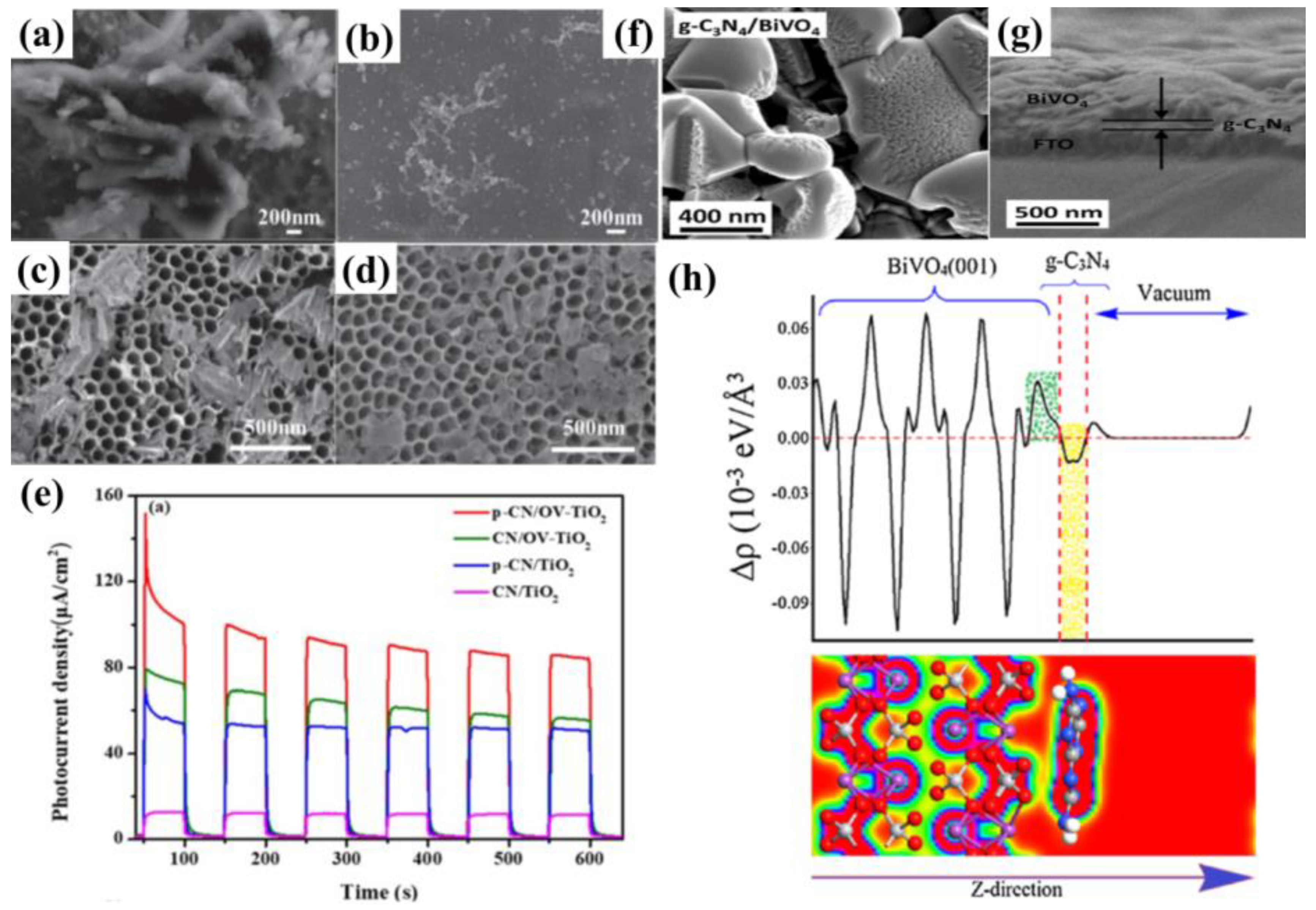
- Liu, C.; Wang, F.; Zhang, J.; Wang, K.; Qiu, Y.; Liang, Q.; Chen, Z. Efficient Photoelectrochemical Water Splitting by g-C3N4/TiO2 Nanotube Array Heterostructures. Nano-Micro Lett. 2018, 10, 37. [Google Scholar] [CrossRef] [PubMed]
- Bhat, S.S.M.; Jun, S.E.; Lee, S.A.; Lee, T.H.; Jang, H.W. Influence of C3N4 Precursors on Photoelectrochemical Behavior of TiO2/C3N4 Photoanode for Solar Water Oxidation. Energies 2020, 13, 974. [Google Scholar] [CrossRef]
- Su, J.; Geng, P.; Li, X.; Zhao, Q.; Quan, X.; Chen, G. Novel phosphorus doped carbon nitride modified TiO2 nanotube arrays with improved photoelectrochemical performance. Nanoscale 2015, 7, 16282–16289. [Google Scholar] [CrossRef]
- Chen, X.; Liu, L.; Yu, P.Y.; Mao, S.S. Increasing Solar Absorption for Photocatalysis with Black Hydrogenated Titanium Dioxide Nanocrystals. Science 2011, 331, 746–750. [Google Scholar] [CrossRef]
- Zhou, S.; Liu, S.; Su, K.; Jia, K. Graphite carbon nitride coupled S-doped hydrogenated TiO2 nanotube arrays with improved photoelectrochemical performance. J. Electroanal. Chem. 2020, 862, 114008. [Google Scholar] [CrossRef]
- Ouyang, W.; Ji, Y.; Tan, S.; Tian, Q.; Tong, Z. Visible-light-response g-C3N4@N,S-TiO2 nanocomposites for superior photocatalysis and photoelectrochemical performance. J. Alloys Compd. 2021, 866, 158964. [Google Scholar] [CrossRef]
- Blaskievicz, S.F.; Santos, H.L.S.; Teixeira, I.F.; Bott-Neto, J.L.; Fernández, P.S.; Mascaro, L.H. Nickel-modified polymeric carbon nitride for improving TiO2-based photoanode: Photoelectrocatalytical evaluation and mechanistical insights. Mater. Today Nano 2022, 18, 100192. [Google Scholar] [CrossRef]
- Mustakim, N.S.M.; Ubani, C.A.; Sepeai, S.; Ludin, N.A.; Teridi, M.A.M.; Ibrahim, M.A. Quantum dots processed by SILAR for solar cell applications. Sol. Energy 2018, 163, 256–270. [Google Scholar] [CrossRef]
- Kouhnavard, M.; Ikeda, S.; Ludin, N.A.; Khairudin, N.B.A.; Ghaffari, B.V.; Mat-Teridi, M.A.; Sopian, K. A review of semiconductor materials as sensitizers for quantum dot-sensitized solar cells. Renew. Sustain. Energy Rev. 2014, 37, 397–407. [Google Scholar] [CrossRef]
- Zhou, J.; Yang, Y.; Zhang, C.-y. A low-temperature solid-phase method to synthesize highly fluorescent carbon nitride dots with tunable emission. Chem. Commun. 2013, 49, 8605–8607. [Google Scholar] [CrossRef] [PubMed]
- Su, J.; Zhu, L.; Chen, G. Ultrasmall graphitic carbon nitride quantum dots decorated self-organized TiO2 nanotube arrays with highly efficient photoelectrochemical activity. Appl. Catal. B. 2016, 186, 127–135. [Google Scholar] [CrossRef]
- Sun, J.-X.; Yuan, Y.-P.; Qiu, L.-G.; Jiang, X.; Xie, A.-J.; Shen, Y.-H.; Zhu, J.-F. Fabrication of composite photocatalyst g-C3N4-ZnO and enhancement of photocatalytic activity under visible light. Dalton Trans. 2012, 41, 6756–6763. [Google Scholar] [CrossRef]
- Li, J.; Zhou, M.; Ye, Z.; Wang, H.; Ma, C.; Huo, P.; Yan, Y. Enhanced photocatalytic activity of g-C3N4-ZnO/HNT composite heterostructure photocatalysts for degradation of tetracycline under visible light irradiation. RSC Adv. 2015, 5, 91177–91189. [Google Scholar] [CrossRef]
- Liu, W.; Wang, M.; Xu, C.; Chen, S. Facile synthesis of g-C3N4/ZnO composite with enhanced visible light photooxidation and photoreduction properties. Chem. Eng. J. 2012, 209, 386–393. [Google Scholar] [CrossRef]
- Fang, Y.; Xu, Y.; Li, X.; Ma, Y.; Wang, X. Coating Polymeric Carbon Nitride Photoanodes on Conductive Y:ZnO Nanorod Arrays for Overall Water Splitting. Angew. Chem. Int. Ed. 2018, 57, 9749–9753. [Google Scholar] [CrossRef]
- Park, T.J.; Pawar, R.C.; Kang, S.; Lee, C.S. Ultra-thin coating of g-C3N4 on an aligned ZnO nanorod film for rapid charge separation and improved photodegradation performance. RSC Adv. 2016, 6, 89944–89952. [Google Scholar] [CrossRef]
- Hajduk, S.; Berglund, S.P.; Podlogar, M.; Drazic, G.; Abdi, F.F.; Orel, Z.C.; Shalom, M. Conformal Carbon Nitride Coating as an Efficient Hole Extraction Layer for ZnO Nanowires-Based Photoelectrochemical Cells. Adv. Mater. Interfaces. 2017, 4, 1700924. [Google Scholar] [CrossRef]
- Mahala, C.; Sharma, M.D.; Basu, M. ZnO Nanosheets Decorated with Graphite-Like Carbon Nitride Quantum Dots as Photoanodes in Photoelectrochemical Water Splitting. ACS Appl. Nano Mater. 2020, 3, 1999–2007. [Google Scholar] [CrossRef]
- Aslam, I.; Cao, C.; Tanveer, M.; Khan, W.S.; Tahir, M.; Abid, M.; Mahmood, N. The synergistic effect between WO3 and g-C3N4 towards efficient visible-light-driven photocatalytic performance. New J. Chem. 2014, 38, 5462–5469. [Google Scholar] [CrossRef]
- Zhan, F.; Xie, R.; Li, W.; Li, J.; Yang, Y.; Li, Y.; Chen, Q. In situ synthesis of g-C3N4/WO3 heterojunction plates array films with enhanced photoelectrochemical performance. RSC Adv. 2015, 5, 69753–69760. [Google Scholar] [CrossRef]
- Okoroafor, E.C.; Maouche, C.; Liu, Q.; Hong, X.; Rao, S.; Umba, F.M.; Yang, J. Rational Design of 0D/2D WO3/g-C3N4 Z-scheme Hybrid for Improving Photocatalytic Dye Degradation. ChemistrySelect 2022, 7, e202102954. [Google Scholar] [CrossRef]
- Li, Y.; Wei, X.; Yan, X.; Cai, J.; Zhou, A.; Yang, M.; Liu, K. Construction of inorganic-organic 2D/2D WO3/g-C3N4 nanosheet arrays toward efficient photoelectrochemical splitting of natural seawater. Phys. Chem. Chem. Phys. 2016, 18, 10255–10261. [Google Scholar] [CrossRef] [PubMed]
- Li, H.; Zhao, F.; Zhang, J.; Luo, L.; Xiao, X.; Huang, Y.; Tong, Y. A g-C3N4/WO3 photoanode with exceptional ability for photoelectrochemical water splitting. Mater. Chem. Front. 2017, 1, 338–342. [Google Scholar] [CrossRef]
- Liu, Y.; Yu, Y.-X.; Zhang, W.-D. Photoelectrochemical study on charge transfer properties of nanostructured Fe2O3 modified by g-C3N4. Int. J. Hydrogen Energy 2014, 39, 9105–9113. [Google Scholar] [CrossRef]
- Liu, Y.; Wang, D.-P.; Yu, Y.-X.; Zhang, W.-D. Preparation and photoelectrochemical properties of functional carbon nanotubes and Ti co-doped Fe2O3 thin films. Int. J. Hydrogen Energy 2012, 37, 9566–9575. [Google Scholar] [CrossRef]
- Liu, Y.; Su, F.-Y.; Yu, Y.-X.; Zhang, W.-D. Nano g-C3N4 modified Ti-Fe2O3 vertically arrays for efficient photoelectrochemical generation of hydrogen under visible light. Int. J. Hydrogen Energy 2016, 41, 7270–7279. [Google Scholar] [CrossRef]
- Dong, Y.; Chen, Y.; Jiang, P.; Wang, G.; Wu, X.; Wu, R. A novel g-C3N4 based photocathode for photoelectrochemical hydrogen evolution. RSC Adv. 2016, 6, 7465–7473. [Google Scholar] [CrossRef]
- Shanker, G.S.; Panchal, R.A.; Ogale, S.; Nag, A. g-C3N4:Sn-doped In2O3 (ITO) nanocomposite for photoelectrochemical reduction of water using solar light. J. Solid State Chem. 2020, 285, 121187. [Google Scholar] [CrossRef]
- Ma, X.; Zhang, J.; Wang, B.; Li, Q.; Chu, S. Hierarchical Cu2O foam/g-C3N4 photocathode for photoelectrochemical hydrogen production. Appl. Surf. Sci. 2018, 427, 907–916. [Google Scholar] [CrossRef]
- Iqbal, N. Ultrasonically anchored MoO3-g-C3N4 photocatalyst for enhanced solar driven hydrogen generation and environmental remediation. J. Photochem. Photobiol. A Chem. 2022, 427, 113813. [Google Scholar] [CrossRef]
- Jumeri, F.A.; Lim, H.N.; Zainal, Z.; Huang, N.M.; Pandikumar, A. Titanium dioxide-reduced graphene oxide thin film for photoelectrochemical water splitting. Ceram. Int. 2014, 40, 15159–15165. [Google Scholar]
- Khamkhash, L.; Em, S.; Molkenova, A.; Hwang, Y.-H.; Atabaev, T.S. Crack-Free and Thickness-Controllable Deposition of TiO2–rGO Thin Films for Solar Harnessing Devices. Coatings 2022, 12, 218. [Google Scholar] [CrossRef]
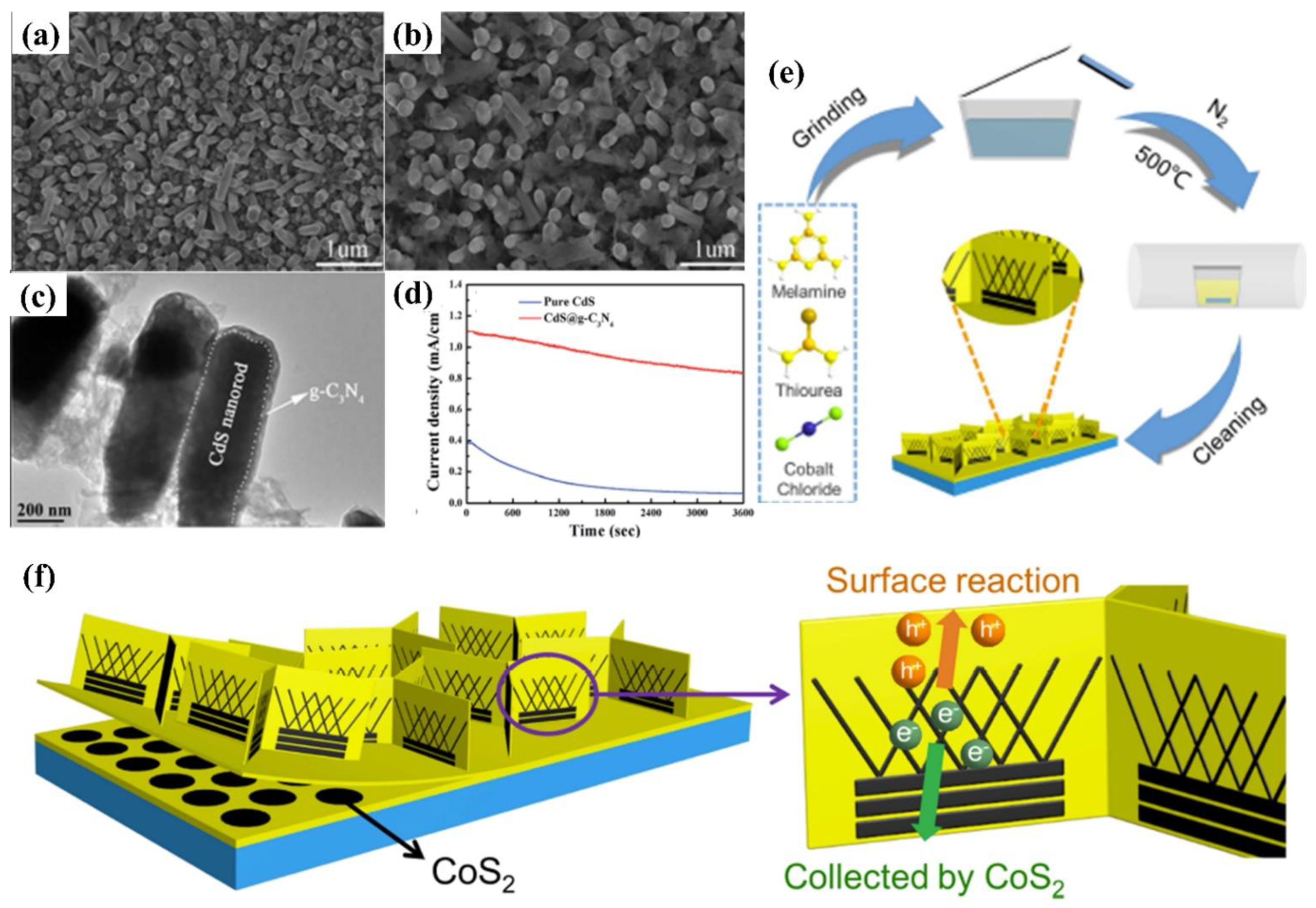
- Li, X.; Wang, J.; Xia, J.; Fang, Y.; Hou, Y.; Fu, X.; Wang, X. One-Pot Synthesis of CoS2 Merged in Polymeric Carbon Nitride Films for Photoelectrochemical Water Splitting. ChemSusChem 2022, 15, e202200330. [Google Scholar] [CrossRef]
- Dai, X.; Xie, M.; Meng, S.; Fu, X.; Chen, S. Coupled systems for selective oxidation of aromatic alcohols to aldehydes and reduction of nitrobenzene into aniline using CdS/g-C3N4 photocatalyst under visible light irradiation. Appl. Catal. B. 2014, 158, 382–390. [Google Scholar] [CrossRef]
- Li, Z.; Liu, Z.; Li, B.; Li, D.; Ge, C.; Fang, Y. Novel CdS nanorods/g-C3N4 nanosheets 1-D/2-D hybrid architectures: An in situ growth route and excellent visible light photoelectrochemical performances. J. Mater. Sci. Mater. Electron. 2016, 27, 2904–2913. [Google Scholar] [CrossRef]
- Zheng, D.; Zhang, G.; Wang, X. Integrating CdS quantum dots on hollow graphitic carbon nitride nanospheres for hydrogen evolution photocatalysis. Appl. Catal. B. 2015, 179, 479–488. [Google Scholar] [CrossRef]
- Li, Y.; Wei, X.; Li, H.; Wang, R.; Feng, J.; Yun, H.; Zhou, A. Fabrication of inorganic-organic core-shell heterostructure: Novel CdS@g-C3N4 nanorod arrays for photoelectrochemical hydrogen evolution. RSC Adv. 2015, 5, 14074–14080. [Google Scholar] [CrossRef]
- Wang, R.; Yan, J.; Zu, M.; Yang, S.; Cai, X.; Gao, Q.; Zhang, S. Facile synthesis of interlocking g-C3N4/CdS photoanode for stable photoelectrochemical hydrogen production. Electrochim. Acta. 2018, 279, 74–83. [Google Scholar] [CrossRef]
- Liu, Y.; Han, J.; Zeng, X.; Tian, Z.; Yu, F.; Sun, X.; Wang, W. g-C3N4 Homophase Junction with High Crystallinity Using MoS2 as Cocatalyst for Robust Visible-Light-Driven Photocatalytic Pollutant Degradation. ChemistrySelect 2022, 7, e202103884. [Google Scholar]
- Ding, J.; Wang, Y.; Guo, S.; Zhang, Y.; Xin, X.; Tang, S.; Li, X. Designing Efficient MoS2/g-C3N4 Hybrid Photocatalysts by Regulating the Interlayer Spacing of MoS2. Eur. J. Inorg. Chem. 2021, 2021, 3719–3726. [Google Scholar] [CrossRef]
- Govinda Raj, M.; Vijayakumar, E.; Preetha, R.; Gnanasekar Narendran, M.; Abigail Jennifer, G.; Varathan, E.; John Bosco, A. Experimental investigation into the π-conjugated HT-g-C3N4/MoS2 (X) evokes the electron transport in type-II heterojunction to achieve high photocatalytic antibiotic removal under visible-light irradiation. Sep. Purif. Technol. 2022, 292, 121028. [Google Scholar] [CrossRef]
- Yuan, H.; Fang, F.; Dong, J.; Xia, W.; Zeng, X.; Shangguan, W. Enhanced photocatalytic hydrogen production based on laminated MoS2/g-C3N4 photocatalysts. Colloids Surf. A. 2022, 641, 128575. [Google Scholar] [CrossRef]
- Ye, L.; Wang, D.; Chen, S. Fabrication and Enhanced Photoelectrochemical Performance of MoS2/S-Doped g-C3N4 Heterojunction Film. ACS Appl. Mater. Interfaces 2016, 8, 5280–5289. [Google Scholar] [CrossRef] [PubMed]
- Liu, Y.; Zhang, J.; Li, X.; Yao, Z.; Zhou, L.; Sun, H.; Wang, S. Graphitic Carbon Nitride Decorated with CoP Nanocrystals for Enhanced Photocatalytic’ and Photoelectrochemical H2 Evolution. Energy Fuels 2019, 33, 11663–11676. [Google Scholar] [CrossRef]
- Alhaddad, M.; Amin, M.S. Removal of ciprofloxacin applying Pt@BiVO4-g-C3N4 nanocomposite under visible light. Opt. Mater. 2022, 124, 111976. [Google Scholar] [CrossRef]
- Tian, Y.; Zhang, J.; Wang, W.; Liu, J.; Zheng, X.; Li, J.; Guan, X. Facile assembly and excellent elimination behavior of porous BiOBr-g-C3N4 heterojunctions for organic pollutants. Environ. Res. 2022, 209, 112889. [Google Scholar] [CrossRef]
- Sariket, D.; Ray, D.; Baduri, S.; Ghosh, S.; Maity, A.; Bhattacharya, C. Synthesis of g-C3N4/InVO4 Semiconductor for Improved Photocatalytic and Photoelectrochemical Applications. Electroanalysis 2020, 32, 2535–2544. [Google Scholar] [CrossRef]
- Wang, M.; Guo, P.; Chai, T.; Xie, Y.; Han, J.; You, M.; Zhu, T. Effects of Cu dopants on the structures and photocatalytic performance of cocoon-like Cu-BiVO4 prepared via ethylene glycol solvothermal method. J. Alloys Compd. 2017, 691, 8–14. [Google Scholar] [CrossRef]
- Mane, P.; Bagal, I.V.; Bae, H.; Burungale, V.; Seong, C.; Ryu, S.W.; Ha, J.S. Bifacial Modulation of Carrier Transport in BiVO4 Photoanode for Stable Photoelectrochemical Water Splitting via Interface Engineering. Adv. Sustain. Syst. 2022, 6, 2200014. [Google Scholar] [CrossRef]
- Wang, Y.; Chen, D.; Zhang, J.; Balogun, M.S.; Wang, P.; Tong, Y.; Huang, Y. Charge Relays via Dual Carbon-Actions on Nanostructured BiVO4 for High Performance Photoelectrochemical Water Splitting. Adv. Funct. Mater. 2022, 32, 2112738. [Google Scholar] [CrossRef]
- Wang, Y.; Sun, J.; Li, J.; Zhao, X. Electrospinning Preparation of Nanostructured g-C3N4/BiVO4 Composite Films with an Enhanced Photoelectrochemical Performance. Langmuir 2017, 33, 4694–4701. [Google Scholar] [CrossRef]
- Feng, C.; Wang, Z.; Ma, Y.; Zhang, Y.; Wang, L.; Bi, Y. Ultrathin graphitic C3N4 nanosheets as highly efficient metal-free cocatalyst for water oxidation. Appl. Catal. B. 2017, 205, 19–23. [Google Scholar] [CrossRef]
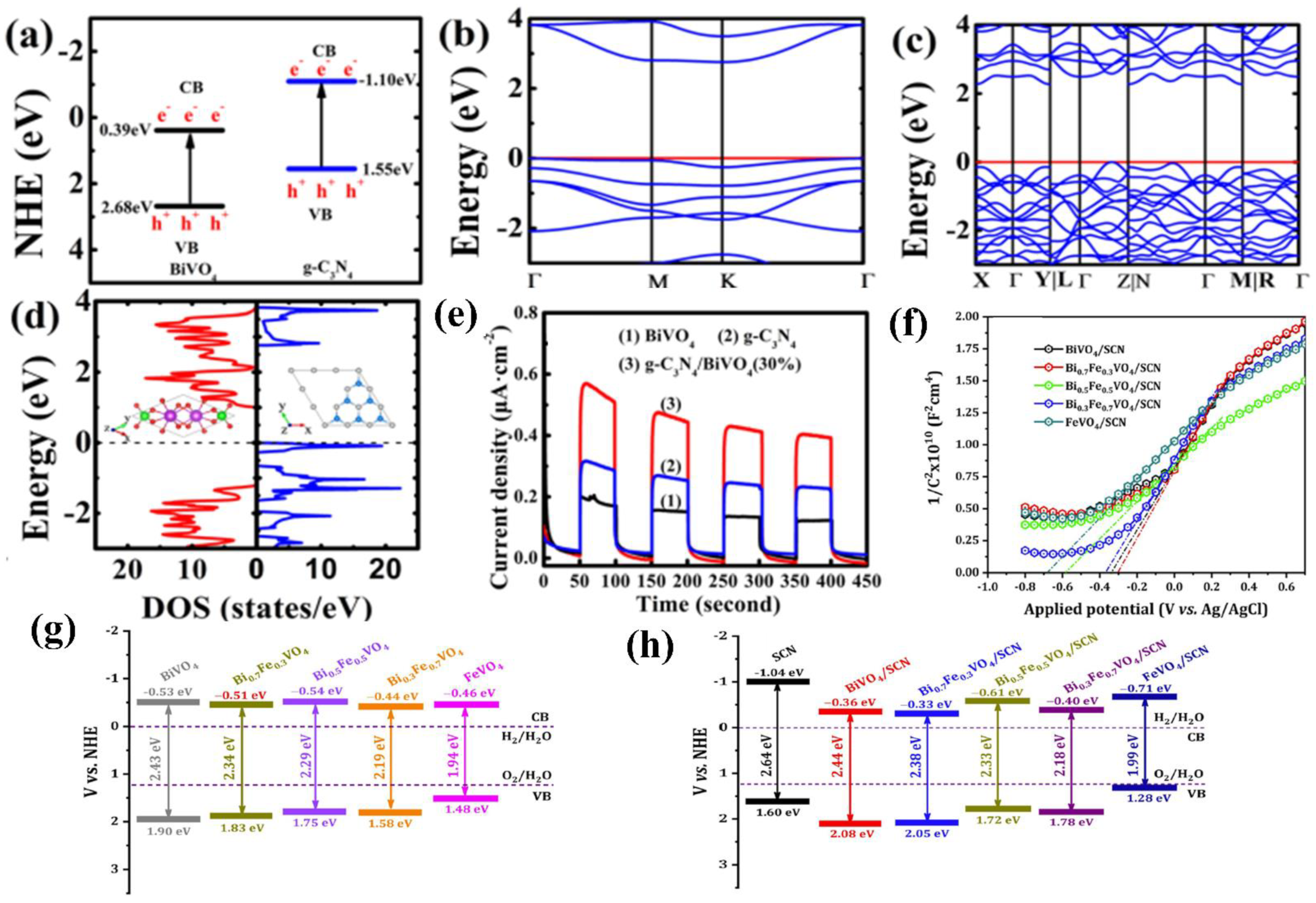
- Jiang, T.; Nan, F.; Zhou, J.; Zheng, F.; Weng, Y.; Cai, T.-Y.; Fang, L. Enhanced photocatalytic and photoelectrochemical performance of g-C3N4/BiVO4 heterojunction: A combined experimental and theoretical study. Aip Adv. 2019, 9, 055225. [Google Scholar] [CrossRef]
- Zeng, G.; Wang, X.; Yu, X.; Guo, J.; Zhu, Y.; Zhang, Y. Ultrathin g-C3N4/Mo:BiVO4 photoanode for enhanced photoelectrochemical water oxidation. J. Power Sources 2019, 444, 227300. [Google Scholar] [CrossRef]
- Balu, S.; Chen, Y.-L.; Chen, S.-W.; Yang, T.C.K. Rational synthesis of BixFe1-xVO4 heterostructures impregnated sulfur-doped g-C3N4: A visible-light-driven type-II heterojunction photo(electro)catalyst for efficient photodegradation of roxarsone and photoelectrochemical OER reactions. Appl. Catal. B. 2022, 304, 120852. [Google Scholar] [CrossRef]
- Rakibuddin, M.; Kim, H.; Khan, M.E. Graphite-like carbon nitride (C3N4) modified N-doped LaTiO3 nanocomposite for higher visible light photocatalytic and photo-electrochemical performance. Appl. Surf. Sci. 2018, 452, 400–412. [Google Scholar] [CrossRef]
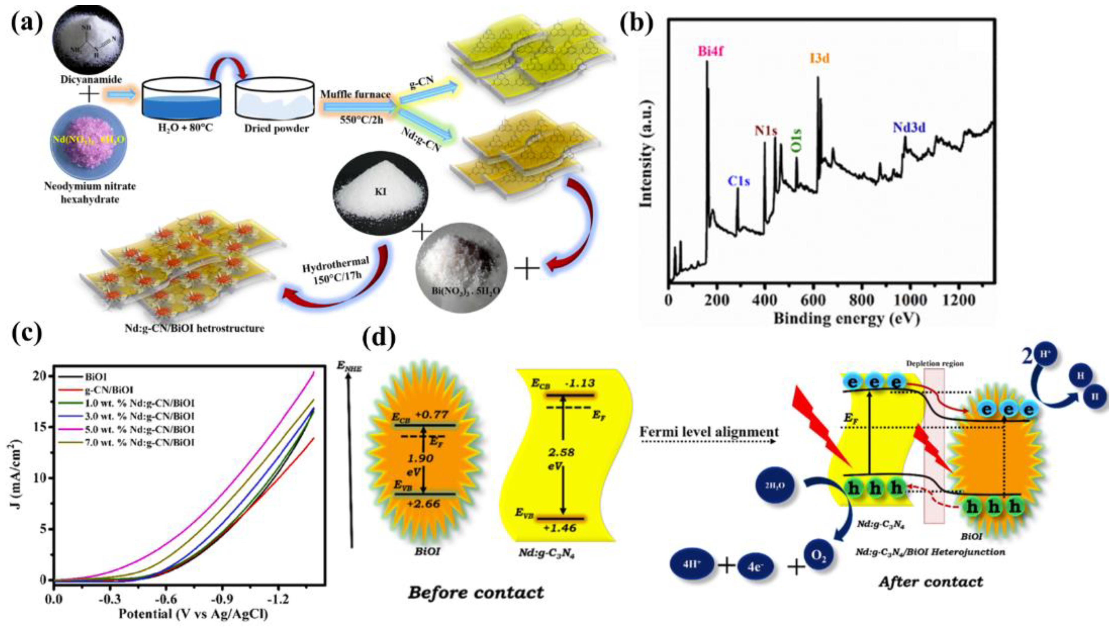
- Velusamy, P.; Sathiya, M.; Liu, Y.; Liu, S.; Ramesh Babu, R.; Aly Saad Aly, M.; Xing, R. Investigating the effect of Nd3+ dopant and the formation of g-C3N4/BiOI heterostructure on the microstructural, optical and photoelectrocatalytic properties of g-C3N4. Appl. Surf. Sci. 2021, 561, 150082. [Google Scholar] [CrossRef]
- Kumar, D.; Sharma, S.; Khare, N. Enhanced photoelectrochemical performance of NaNbO3 nanofiber photoanodes coupled with visible light active g-C3N4 nanosheets for water splitting. Nanotechnology 2020, 31, 135402. [Google Scholar] [CrossRef] [PubMed]
- Yang, F.; Kuznietsov, V.; Lublow, M.; Merschjann, C.; Steigert, A.; Klaer, J.; Schedel-Niedrig, T. Solar hydrogen evolution using metal-free photocatalytic polymeric carbon nitride/CuInS2 composites as photocathodes. J. Mater. Chem. A 2013, 1, 6407–6415. [Google Scholar] [CrossRef]
- Gandamalla, A.; Manchala, S.; Anand, P.; Fu, Y.-P.; Shanker, V. Development of versatile CdMoO4/g-C3N4 nanocomposite for enhanced photoelectrochemical oxygen evolution reaction and photocatalytic dye degradation applications. Mater. Today Chem. 2021, 19, 100392. [Google Scholar] [CrossRef]
- Xu, T.; Niu, P.; Wang, S.; Li, L. High visible light photocatalytic activities obtained by integrating g-C3N4 with ferroelectric PbTiO3. J. Mater. Sci. Technol. 2021, 74, 128–135. [Google Scholar] [CrossRef]
- Xiao, T.; Tang, Z.; Yang, Y.; Tang, L.; Zhou, Y.; Zou, Z. In situ construction of hierarchical WO3/g-C3N4 composite hollow microspheres as a Z-scheme photocatalyst for the degradation of antibiotics. Appl. Catal. B. 2018, 220, 417–428. [Google Scholar] [CrossRef]
- She, X.; Wu, J.; Xu, H.; Zhong, J.; Wang, Y.; Song, Y.; Ajayan, P.M. High Efficiency Photocatalytic Water Splitting Using 2D alpha-Fe2O3/g-C3N4 Z-Scheme Catalysts. Adv. Energy Mater. 2017, 7, 1700025. [Google Scholar] [CrossRef]
- Li, J.; Yuan, H.; Zhu, Z. Improved photoelectrochemical performance of Z-scheme g-C3N4/Bi2O3/BiPO4 heterostructure and degradation property. Appl. Surf. Sci. 2016, 385, 34–41. [Google Scholar] [CrossRef]
- Li, J.; Hao, H.; Zhu, Z. Construction of g-C3N4-WO3-Bi2WO6 double Z-scheme system with enhanced photoelectrochemical performance. Mater. Lett. 2016, 168, 180–183. [Google Scholar] [CrossRef]
- Pan, C.; Jia, J.; Hu, X.; Fan, J.; Liu, E. In situ construction of g-C3N4/TiO2 heterojunction films with enhanced photocatalytic activity over magnetic-driven rotating frame. Appl. Surf. Sci. 2018, 430, 283–292. [Google Scholar] [CrossRef]
- Xiao, L.; Liu, T.; Zhang, M.; Li, Q.; Yang, J. Interfacial Construction of Zero-Dimensional/One-Dimensional g-C3N4 Nanoparticles/TiO2 Nanotube Arrays with Z-Scheme Heterostructure for Improved Photoelectrochemical Water Splitting. ACS Sustain. Chem. Eng. 2019, 7, 2483. [Google Scholar] [CrossRef]
- Xiao, L.; Zhu, H.; Zhang, M.; Yang, X.; Li, Q.; Yang, J. Enhanced Photoelectrochemical Performance of g-C3N4/TiO2 Heterostructure by the Cooperation of Oxygen Vacancy and Protonation Treatment. J. Electrochem. Soc. 2020, 167, 066513. [Google Scholar] [CrossRef]
- Murugan, C.; Nataraj, R.A.; Kumar, M.P.; Ravichandran, S.; Pandikumar, A. Enhanced Charge Transfer Process of Bismuth Vanadate Interleaved Graphitic Carbon Nitride Nanohybrids in Mediator-Free Direct Z Scheme Photoelectrocatalytic Water Splitting. Chemistryselect 2019, 4, 4653–4663. [Google Scholar] [CrossRef]
- Han, J.-M.; Wu, N.; Wang, B.; Wang, C.; Xu, M.; Yang, X.; Zang, L. gamma radiation induced self-assembly of fluorescent molecules into nanofibers: A stimuli-responsive sensing. J. Mater. Chem. C. 2015, 3, 4345–4351. [Google Scholar] [CrossRef]
- Park, J.-E.; Kim, K.-Y.; Choi, W.-H.; Lee, H.; Cho, S.-J.; Ahn, S.-H.; Kim, J.-Y.; Song, Y.-K.; Kim, K.-B.; Huh, H.-D.; et al. Evaluation of Fabricated Semiconductor Sensor for Verification of γ-ray Distribution in Brachytherapy. Prog. Med. Phys. 2015, 26, 280–285. [Google Scholar] [CrossRef][Green Version]
- Mohamed, N.A.; Ullah, H.; Safaei, J.; Ismail, A.F.; Noh, M.F.M.; Soh, M.F.; Teridi, M.A.M. Efficient Photoelectrochemical Performance of gamma Irradiated g-C3N4 and Its g-C3N4@BiVO4 Heterojunction for Solar Water Splitting. J. Mater. Chem. C. 2019, 123, 9013–9026. [Google Scholar]
- Qu, Y.; Zhou, W.; Ren, Z.; Du, S.; Meng, X.; Tian, G.; Fu, H. Facile preparation of porous NiTiO3 nanorods with enhanced visible-light-driven photocatalytic performance. J. Mater. Chem. 2012, 22, 16471–16476. [Google Scholar] [CrossRef]
- Inceesungvorn, B.; Teeranunpong, T.; Nunkaew, J.; Suntalelat, S.; Tantraviwat, D. Novel NiTiO3/Ag3VO4 composite with enhanced photocatalytic performance under visible light. Catal. Commun. 2014, 54, 35–38. [Google Scholar] [CrossRef]
- Anandan, S.; Lana-Villarreal, T.; Wu, J.J. Sonochemical Synthesis of Mesoporous NiTiO3 Ilmenite Nanorods for the Catalytic Degradation of Tergitol in Water. Ind. Eng. Chem. Res. 2015, 54, 2983–2990. [Google Scholar] [CrossRef]
- Wang, H.; Yuan, X.; Wang, H.; Chen, X.; Wu, Z.; Jiang, L.; Zeng, G. One-step calcination method for synthesis of mesoporous g-C3N4/NiTiO3 heterostructure photocatalyst with improved visible light photoactivity. RSC Adv. 2015, 5, 95643–95648. [Google Scholar] [CrossRef]
- Zeng, Y.; Wang, Y.; Chen, J.; Jiang, Y.; Kiani, M.; Li, B.; Wang, R. Fabrication of high-activity hybrid NiTiO3/g-C3N4 heterostructured photocatalysts for water splitting to enhanced hydrogen production. Ceram. Int. 2016, 42, 12297–12305. [Google Scholar] [CrossRef]
- Huang, Z.; Zeng, X.; Li, K.; Gao, S.; Wang, Q.; Lu, J. Z-Scheme NiTiO3/g-C3N4 Heterojunctions with Enhanced Photoelectrochemical and Photocatalytic Performances under Visible LED Light Irradiation. ACS Appl. Mater. Interfaces 2017, 9, 41120–41125. [Google Scholar] [CrossRef] [PubMed]
- Xiao, J.; Zhang, X.; Li, Y. A ternary g-C3N4/Pt/ZnO photoanode for efficient photoelectrochemical water splitting. Int. J. Hydrogen Energy 2015, 40, 9080–9087. [Google Scholar] [CrossRef]
- Wen, P.; Sun, Y.; Li, H.; Liang, Z.; Wu, H.; Zhang, J.; Jiang, L. A highly active three-dimensional Z-scheme ZnO/Au/g-C3N4 photocathode for efficient photoelectrochemical water splitting. Appl. Catal. B. 2020, 263, 118180. [Google Scholar] [CrossRef]
- Guo, B.; Zhao, C.; Zhou, L.; Yu, Z.; Liu, X.; Zhao, Z.; Yuan, H. Constructing a novel multi-hierarchical TiO2/g-C3N4/Ag-AgBr photocatalyst with dual Z-scheme heterojunction utilizing Ag as the charge transfer mediator. J. Alloys Compd. 2022, 900, 163514. [Google Scholar] [CrossRef]
- Reddy, A.S.; Kim, J. An efficient g-C3N4-decorated CdS-nanoparticle-doped Fe3O4 hybrid catalyst for an enhanced H2 evolution through photoelectrochemical water splitting. Appl. Surf. Sci. 2020, 513, 145836. [Google Scholar] [CrossRef]
- Si, H.; Deng, Q.; Yin, C.; Tavakoli, M.M.; Zhang, J.; Kong, J. Graphdiyne Coupled with g-C3N4/NiFe-Layered Double Hydroxide, a Layered Nanohybrid for Highly Efficient Photoelectrochemical Water Oxidation. Adv. Mater. Interfaces 2020, 7, 1902083. [Google Scholar] [CrossRef]
- Guru, S.; Rao, R.G. Bismuth oxycarbonate grafted NiFe-LDH supported on g-C3N4 as bifunctional catalyst for photoelectrochemical water splitting. Int. J. Hydrogen Energy 2021, 46, 12145–12157. [Google Scholar] [CrossRef]
- Guru, S.; Kumar, S.; Bellamkonda, S.; Gangavarapu, R.R. Synthesis of CuTi-LDH supported on g-C3N4 for electrochemical and photoelectrochemical oxygen evolution reactions. Int. J. Hydrogen Energy 2021, 46, 16414–16430. [Google Scholar] [CrossRef]
- Yu, Z.; Li, Y.; Qu, J.; Zheng, R.; Cairney, J.M.; Zhang, J.; Li, W. Enhanced photoelectrochemical water-splitting performance with a hierarchical heterostructure: Co3O4 nanodots anchored TiO2@P-C3N4 coreshell nanorod arrays. Chem. Eng. J. 2021, 404, 126458. [Google Scholar] [CrossRef]
- Liu, C.; Qiu, Y.; Zhang, J.; Liang, Q.; Mitsuzaki, N.; Chen, Z. Construction of CdS quantum dots modified g-C3N4/ZnO heterostructured photoanode for efficient photoelectrochemical water splitting. J. Photochem. Photobiol., A. 2019, 371, 109–117. [Google Scholar] [CrossRef]
- Bashiri, R.; Mohamed, N.M.; Suhaimi, N.A.; Shahid, M.U.; Kait, C.F.; Sufian, S.; Mumtaz, A. Photoelectrochemical water splitting with tailored TiO2/SrTiO3@g-C3N4 heterostructure nanorod in photoelectrochemical cell. Diamond Relat. Mater. 2018, 85, 5–12. [Google Scholar] [CrossRef]
- Gopalakrishnan, S.; Bhalerao, G.M.; Jeganathan, K. SrTiO3 NPs/g-C3N4 NSs Coupled Si NWs based Hybrid Photocathode for Visible Light Driven Photoelectrochemical Water Reduction. ACS Sustain. Chem. Eng. 2019, 7, 13911–13919. [Google Scholar] [CrossRef]
- Xu, X.; Liu, Y.; Zhu, Y.; Fan, X.; Li, Y.; Zhang, F.; Peng, W. Fabrication of a Cu2O/g-C3N4/WS2 Triple-Layer Photocathode for Photoelectrochemical Hydrogen Evolution. Chemelectrochem 2017, 4, 1498–1502. [Google Scholar] [CrossRef]
- Bhandary, N.; Singh, A.P.; Ingole, P.P.; Basu, S. Enhancing the Photoelectrochemical Performance of a Hematite Dendrite/Graphitic Carbon Nitride Nanocomposite through Surface Modification with CoFeOx. Chemphotochem 2017, 1, 70–75. [Google Scholar] [CrossRef]


| Synthesis Methods | Advantages | Disadvantages |
|---|---|---|
| Thermal vapor condensation (TVC) | (i) Facile and inexpensive. (ii) Produced uniform and dense g−CN film. | (i) Limited precursors (Other frequently reported precursors fail to form g−CN films on solid substrates). (ii) Limited thickness. (iii) The temperature of deposition is limited by the different substrates. |
| solvothermal | (i) Uniform deposition. (ii) Controllable thickness. | (i) Complicated preparation process. (ii) The requirement of long reaction times. (iii) Produced g−CN film with rich surface defects. |
| Liquid-mediated growth | (i) Very facile and cheap to perform. (ii) Strong adhesion of the g−CN film to the substrate. | (i) The temperature of deposition is limited by the different substrate and precursor evaporation. (ii) Hard to control the film thickness. |
| Seed growth | (i) Facile and inexpensive. | (i) Complicated preparation process. (ii) Produced g−CN film with high roughness. |
| Electrochemical deposition | (i) The temperature of deposition is not limited by the different substrates. | (i) Hard to produce a uniform g−CN film. (ii) Physical adhesion of g−CN to the different substrates. |
| Disperse coating | (i) Facile and cost-effective. (ii) Continuous, homogeneous coating formed on various substrates. (iii) Easy to control the film thickness. (iiii) The temperature of deposition is not limited by the different substrates. | (i) The film is easy to fall off. (ii) Limited scalability due to the poor solubility of g−CN powder in most solvents. (iii) Physical adhesion of g−CN to the different substrates. (iiii) Produced g−CN film with rich surface defects. |
| Anodic aluminum oxide membrane deposition | (i) Continuous, homogeneous coating formed on various substrates. (ii) Controllable thickness | (i) Complicated preparation process. |
| electrospinning | (i) Facile. (ii) Controllable thickness. | (i) Weak adhesion of the g−CN film to the substrate. (ii) The stability of the organic matrix is lower than pure g−CN. |
| vacuum magnetic filtered arc ion plating | (i) Facile. (ii) Controllable thickness. (iii) Prepared g−CN film with relatively high crystallinity. | (i) Expensive equipment. (ii) Plasma instability. |
| Radio frequency magnetron-based sputtering | (i) Facile and highly efficient. (ii) Prepared g−CN film with relatively high crystallinity. (iii) Controllable thickness. | (i) Expensive equipment. (ii) Plasma instability. |
| Method | Precursor | Photoelectrode | Potential (V) | J (μA cm−2) | Electrolyte | Light Source | Ref. |
|---|---|---|---|---|---|---|---|
| TVC | melamine | g−CN | 1.55 vs. RHE | 120 | 0.1 M Na2SO4 + 0.01 M Na2S + 0.1 M Na2SO3 | AM 1.5 | [48] |
| TVC | dicyanamide | g−CN | 1.23 vs. RHE | 63 | 0.1 M Na2SO4 | AM 1.5 | [49] |
| SR | cyanuric chloride + melamine | g−CN | 1.23 vs. RHE | 3.5 | 0.2 M Na2SO4 | Visible light (λ ≥ 420 nm) | [57] |
| SR | cyanuric chloride + cyanuric acid | g−CN | 1.23 vs. RHE | 10 | 0.5 M Na2SO4 | AM 1.5 | [58] |
| LMG | Melamine + Trithiocyanuric acid | g−CN@sulfur | 1.23 vs. RHE | 100 | 1.0 M NaOH | AM 1.5 | [64] |
| LMG | 2,4−diamino−6−phenyl−1,3,5−triazine + Cyanuric acid + Ni chloride salt | g−CN:nickel | 1.23 vs. RHE | 69 | 0.1 M KOH | AM 1.5 | [65] |
| SG | Melamine | g−CN | 1.23 vs. RHE | 116 | 0.1 M KOH | AM 1.5 | [66] |
| EPD | cyanuric acid-melamine | Carbon fiber/g−CN | 0 vs. Ag/AgCl | 12 | 1 M KOH | 50 W white LED (λ > 410 nm) | [71] |
| ESP | Dicyandiamide + PVP | g−CN@PVP | 0.5 vs. SCE | 6.64 | 0.05 M Na2SO4 | AM 1.5 | [77] |
| AAO | cyanamide | g−CN | 1.23 vs. RHE | 30.2 | 0.1 M Na2SO4 | AM 1.5 | [90] |
| VMFAIP | Graphite targets and nitrogen gas | g−CN | 1.23 vs. RHE | 10.8 | 0.5 M Na2SO4 | AM 1.5 | [93] |
| RFM | g−CN pellet targets + Ar plasma | g−CN/TiO2 | 0.9 V vs. Ag/AgCl | 290 | 10 mM NaOH | Visible light (l > 420 nm) | [95] |
| Photoelectrode | Dopant/g−CN Precursor | Potential (V) | J (μA cm−2) | Electrolyte | Light Source | Ref. |
|---|---|---|---|---|---|---|
| C/g−CN | 2,6−Diaminopyridine | 1.23 vs. RHE | 100 | 0.1 M Na2SO4 + 0.01 M Na2S + 0.1 M Na2SO3 | AM 1.5 | [53] |
| Ag/g−CN | AgNO3 | 1 V vs. RHE | 6.40 μA/mm2 | 0.05 M Na2SO4 | Visible light (l > 420 nm) | [102] |
| Pd/g−CN | Pd(NO3)2 | 1.23 vs. RHE | 79.2 | 0.5 M Na2SO4 | Visible light (l > 420 nm) | [103] |
| B/g−CN | H3BO3 | 1.23 vs. RHE | 55 | 0.2 M Na2SO4 + 0.05 M Na2S | AM 1.5 | [106] |
| P/g−CN | hexachlorocyclot-riphosphazene | 1.23 vs. RHE | 120 | 1 M NaOH | AM 1.5 | [114] |
| S/g−CN | ammonium thiocyanate | 1.23 vs. RHE | 110 | 1 M NaOH | AM 1.5 | [116] |
| K&I/g−CN | KI + I2 | 0.5 V versus Ag/AgCl | 50.3 | 0.25 M Na2S + 0.35 M Na2SO3 | Visible light (l > 420 nm) | [121] |
| layered-doped g−CN | H3BO3+H3PO4 | 1.23 vs. RHE | 150 ± 10 | 0.1 M Na2SO4 | AM 1.5 | [122] |
| g−CN | melamine+2,6−diaminopyridine (26D) | 1.23 vs. RHE | 100 | 0.1 M Na2SO4 + 0.1 M Na2SO3 + 0.01 M Na2S | AM 1.5 | [53] |
| g−CN | melamine + cyanuric chloride | 1.23 vs. RHE | 230 | 0.5 M Na2SO4 | AM 1.5 | [134] |
| g−CN | Melamine + formaldehyde | 1.23 vs. RHE | 228.2 | 0.2 M Na2SO4 | AM 1.5 | [135] |
| C3N5/TiO2 | Melamine + hydrazine hydrate | 1.23 vs. RHE | 152 | 0.1 M Na2SO4 | AM 1.5 | [136] |
| g−CN/TiO2 | Melamine + hydrazine hydrate | 1.23 vs. RHE | 100 | 0.1 M Na2SO4 | AM 1.5 | [136] |
| g−CN g−CN/FeOOH | thiourea urea | 1.1 vs. RHE 1.1 vs. RHE | 89 122 | 0.1 M Na2SO4 0.1 M Na2SO4 | AM 1.5 AM 1.5 | [51] |
| g−CN/NiCo-LH | cyanuric chloride melamine | 0.6 V vs. SCE | 11.8 | 0.2 M Na2SO4 | 200 W xenon lamp | [51] |
| g−CN g−CN@CNT | melamine | 0 vs. SCE 0 vs. SCE | 0.5 1.8 | 0.5 M Na2SO4 0.5 M Na2SO4 | ZOLIX, 150 W, AAA | [91] |
| DPCN/NRGO/NiFe-LDH | urea+hydrogenation treatment | 1.4 vs. Ag/AgCl | 162.3 | 0.01 M Na2SO4 | AM 1.5 | [142] |
| CN-rGO | cyanuric acid melamine | 1.23 vs. RHE 1.23 vs. RHE | 72 660 | 0.1 M KOH 0.1 M KOH + 10% (v/v) TEOA | AM 1.5 AM 1.5 | [145] |
| Photoelectrode | Composite Type | Potential (V) | J (μA cm−2) | Electrolyte | Illumination | Ref |
|---|---|---|---|---|---|---|
| mesoporous TiO2/g−CN | Type II | 1.23 V vs. RHE | 320 | 0.5 M Na2SO4 | AM 1.5 | [167] |
| mesoporous TiO2/g−CN | Type II | 0 vs. Ag/AgCl | 1400 | 0.1 M Na2S | Visible light (l > 410 nm) | [168] |
| g−CN/TNTA | Type II | 1.23 V vs. RHE | 860 | 0.1 M Na2SO4 | AM 1.5 | [174] |
| TiO2/g−CN | Type II | 1.23 V vs. RHE | 2740 | 1 M NaOH | AM 1.5 | [175] |
| P-CN/TiO2 NTs | Type II | 0 V vs. Ag/AgCl | 1980 | 1 M NaOH | AM 1.5 | [176] |
| g−CN/H-S−TiO2 NTAs | Type II | 1.23 V vs. RHE | 1640 | 1 M KOH | AM 1.5 | [178] |
| CNQDs/TiO2 NTAs | Type II | 0.3 V vs. Ag/AgCl | 1340 | 0.1 M Na2SO4 | AM 1.5 | [184] |
| Y:ZnO/g−CN | Type II | 1.23 vs. RHE | 400 | 0.5 M Na2SO4 | AM 1.5 | [188] |
| ZnONW/g−CN | Type II | 1.23 vs. RHE | 250 | 0.1 M KOH | AM 1.5 | [190] |
| ZnO/g−CN−QDs | Type II | 0.5994 V versus RHE | 952 | 0.5 M Na2SO4 | AM 1.5 | [191] |
| g−CN/Ti−Fe2O3 | Type II | 1.23 vs. RHE | 2550 | 1 M NaOH | 150 mW/cm2 | [193] |
| g−CN/WO3 | Type II | +2.0 V vs. RHE | 2100 | 0.2 M Na2SO4 | AM 1.5 | [194] |
| WO3/g−CN NSAs | Type II | 1.23 vs. RHE | 730 | Sea water | AM 1.5 | [195] |
| g−CN/WO3 | Type II | 1.23 vs. RHE | 1920 | 0.1 M KH2PO4 | AM 1.5 | [196] |
| g−CN/Fe2O3 | Type II | 1.23 vs. RHE | 800 | 1 M NaOH | 150 mW/cm2 | [197] |
| CdS NRs/g−CN NSs | Type II | 1.23 vs. RHE | 100 | 0.05 M Na2SO4 | 150 mW/cm2 | [208] |
| CdS@g−CN CSNRs | Type II | 0.9 vs. RHE | 1160 | 0.35 M Na2SO3 +0.25 M Na2S | AM 1.5 | [210] |
| g−CN/CdS | Type II | 0.0 V bias vs. Ag/AgCl | 5400 | 0.5 M Na2S +0.5 MNa2SO3 | AM 1.5 | [211] |
| MoS2/S-doped g−CN | Type II | 0.5 vs. SCE (+0.5 V vs. Ag/AgCl) | 120 | 0.1 M Na2SO4 | AM 1.5 | [216] |
| CoP/g−CN | Type II | +0.40 V (versus Ag/AgCl) | 150 | 0.05 M Na2SO4 | AM 1.5 | [217] |
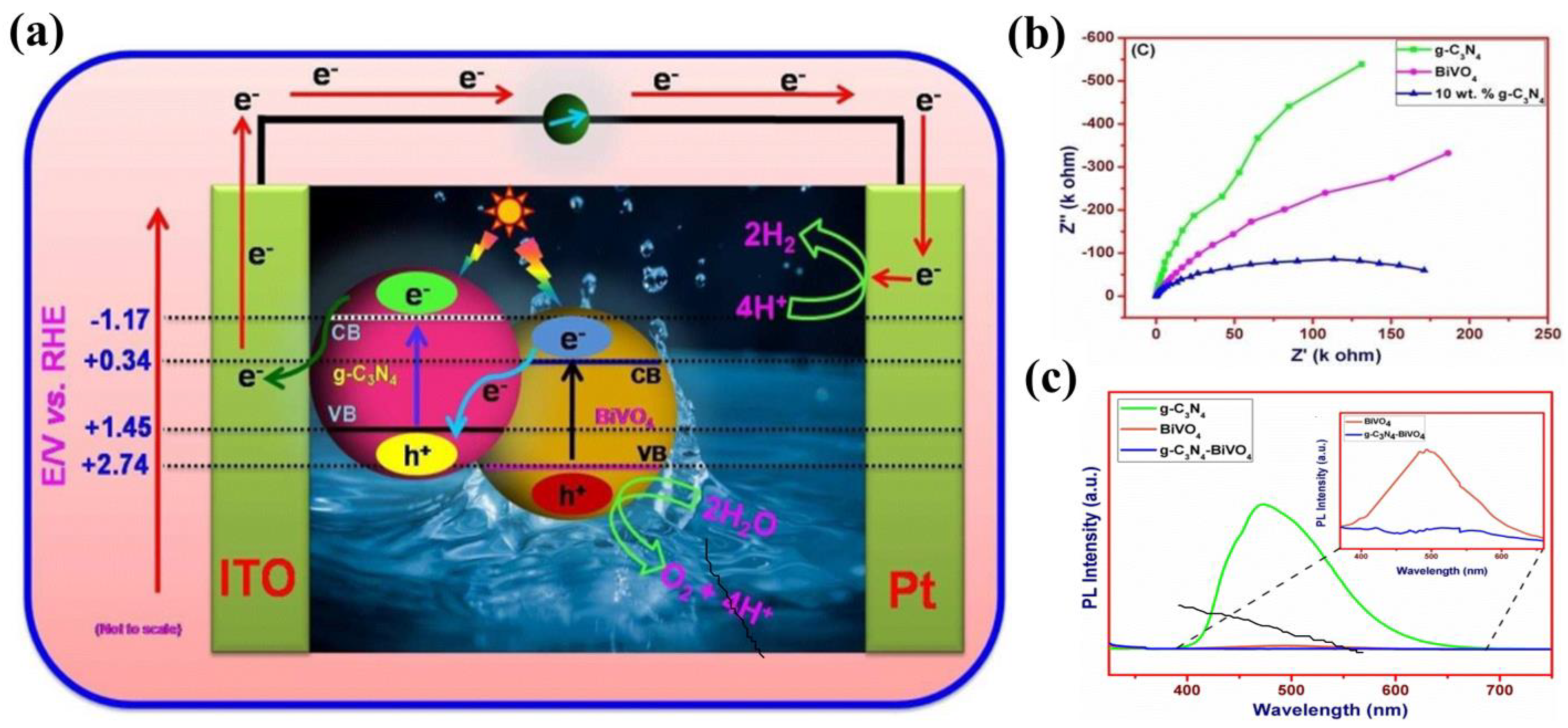
| g−CN/BiVO4 | Type II | 1.23 vs. RHE | 440 | 0.5 M KH2PO4+ 1 M Na2SO3 | Visible light (l > 420 nm) | [224] |
| BiVO4/g−CN−NS | Type II | 1.23 vs. RHE | 3120 | 0.1 M Na2SO4 | Visible light (l > 420 nm) | [225] |
| g−CN/Mo: BiVO4 | Type II | 1.23 vs. RHE | 3110 | 0.1 M KH2PO4 | AM 1.5 | [227] |
| 0D/1D g−CN/OV−TiO2 | Z-Scheme | 1.23 vs. RHE | 720 | 0.1 M Na2SO4 | Visible light (l > 420 nm) | [240] |
| p-CN/OV–TiO2 | Z-Scheme | 0.6 V vs. SCE. | 96 | 0.1 M Na2SO4 | Visible light (l > 420 nm) | [241] |
| g−CN−BiVO4 | Z-Scheme | 1.23 vs. RHE | 2.02 | 1 M KOH | AM 1.5 | [242] |
| g−CN/BiVO4 | Z-Scheme | 1.23 vs. RHE | 420 | 0.5 M Na2SO4 | AM 1.5 | [35] |
| g−CN@BiVO4 | Z-Scheme | 1.23 vs. RHE | 1380 | 0.5 M Na2SO4 | AM 1.5 | [245] |
| NiTiO3/g−CN | Z-Scheme | 1.23 vs. RHE | 250 | 0.1 M Na2SO4 | 30 W visible–light LED | [251] |
| g−CN/Pt/ZnO | Semiconductor-conductor−semiconductor Z-scheme | 0.5 V vs. Ag/AgCl | 120 | 0.5 M Na2SO4 | AM 1.5 | [252] |
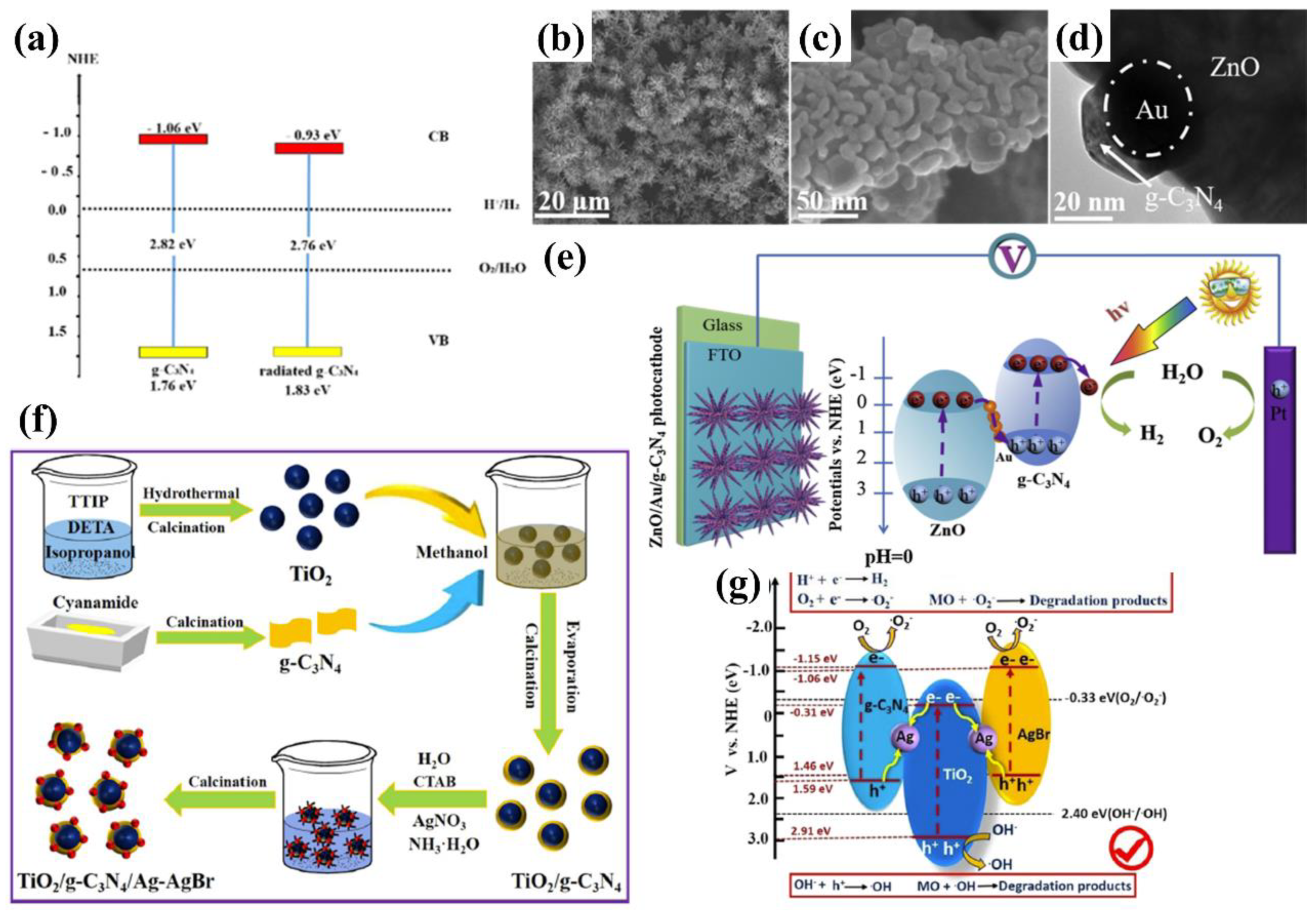
| ZnO/Au/g−CN | Semiconductor-conductor−semiconductor Z-scheme | 0 V vs. RHE | −290 | 0.2 M Na2SO4 | AM 1.5 | [253] |
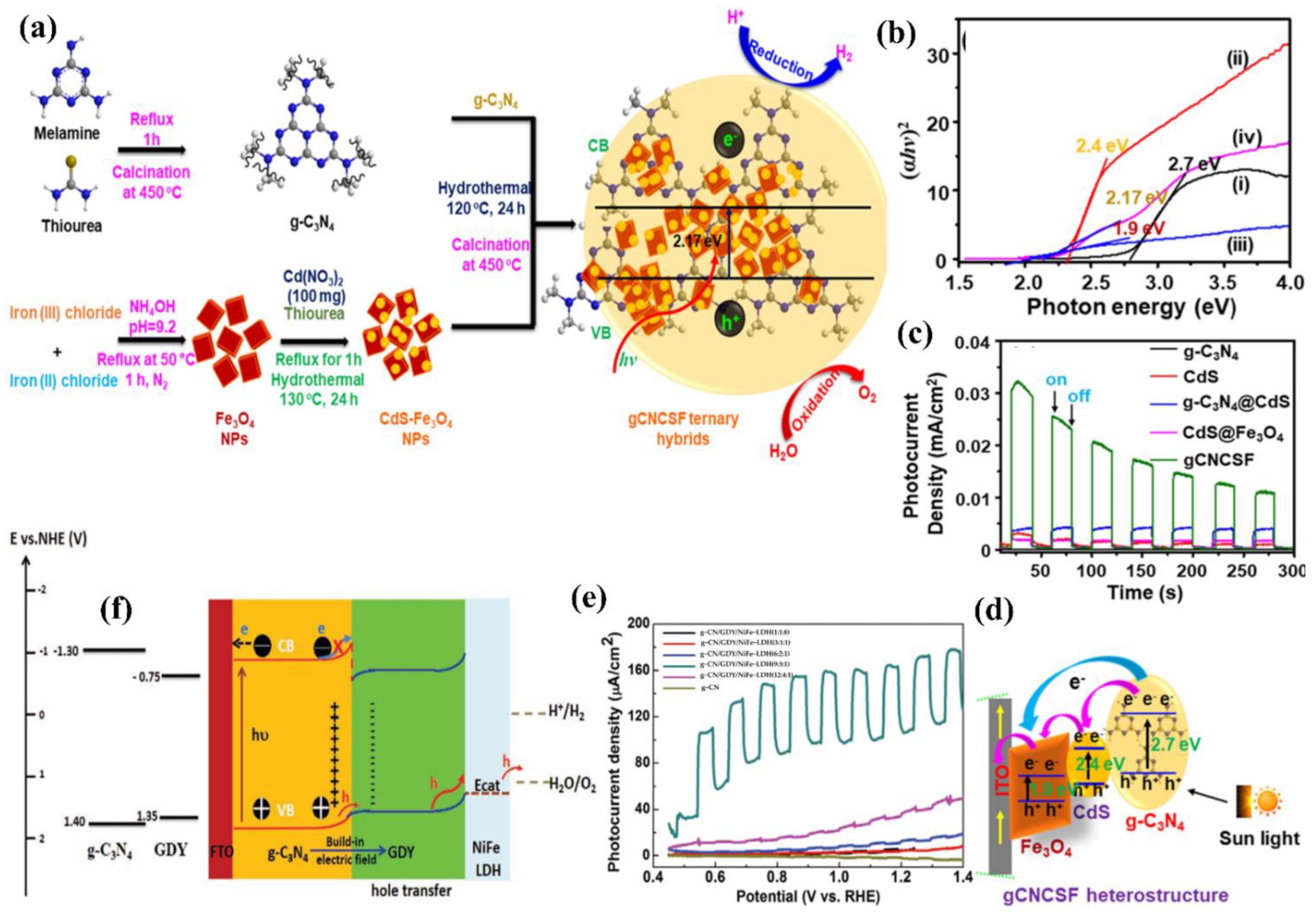
| g−CN@CdS–Fe3O4 | ternary | 0.2 V vs. Ag/AgCl | 23 | 0.5 M Na2SO4 | AM 1.5 | [255] |
| g−CN/GDY/NiFe-LDH | ternary | 1.4 V | 178.66 | 0.01 M Na2SO4 | AM 1.5 | [256] |
| CdS/g−CN/ZnO | ternary | 1.23 vs. RHE | 3340 | 0.1 M Na2S + 0.2 M Na2SO3 | Visible light (l > 420 nm) | [260] |
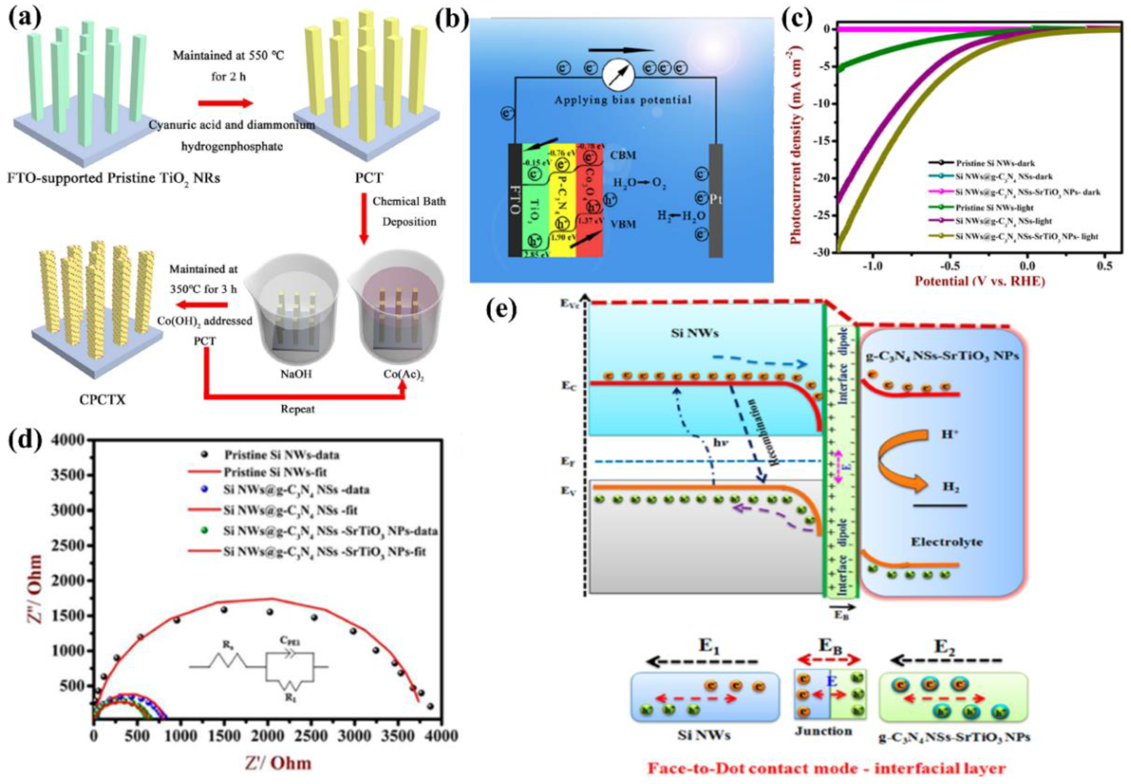
| SiNWs@g−CNNSs−SrTiO3 NPs | ternary | 1.23 vs. RHE | −28,000 | 0.5 MNa2SO4 | AM 1.5 | [262] |
| Cu2O/g−CN/WS2 | ternary | −0.55 vs. RHE | −9500 | 1 M Na2SO4 | Visible light (l > 420 nm) | [263] |
| CoFeOx/HD/g−CN | ternary | 1.23 vs. RHE | 600 | 1MNaOH | Visible light (l > 420 nm) | [264] |
Publisher’s Note: MDPI stays neutral with regard to jurisdictional claims in published maps and institutional affiliations. |
© 2022 by the authors. Licensee MDPI, Basel, Switzerland. This article is an open access article distributed under the terms and conditions of the Creative Commons Attribution (CC BY) license (https://creativecommons.org/licenses/by/4.0/).
Share and Cite
Zhu, Y.; He, L.; Ni, Y.; Li, G.; Li, D.; Lin, W.; Wang, Q.; Li, L.; Yang, H. Recent Progress on Photoelectrochemical Water Splitting of Graphitic Carbon Nitride (g−CN) Electrodes. Nanomaterials 2022, 12, 2374. https://doi.org/10.3390/nano12142374
Zhu Y, He L, Ni Y, Li G, Li D, Lin W, Wang Q, Li L, Yang H. Recent Progress on Photoelectrochemical Water Splitting of Graphitic Carbon Nitride (g−CN) Electrodes. Nanomaterials. 2022; 12(14):2374. https://doi.org/10.3390/nano12142374
Chicago/Turabian StyleZhu, Ying, Liang He, Yiqiang Ni, Genzhuang Li, Dongshuai Li, Wang Lin, Qiliang Wang, Liuan Li, and Haibin Yang. 2022. "Recent Progress on Photoelectrochemical Water Splitting of Graphitic Carbon Nitride (g−CN) Electrodes" Nanomaterials 12, no. 14: 2374. https://doi.org/10.3390/nano12142374
APA StyleZhu, Y., He, L., Ni, Y., Li, G., Li, D., Lin, W., Wang, Q., Li, L., & Yang, H. (2022). Recent Progress on Photoelectrochemical Water Splitting of Graphitic Carbon Nitride (g−CN) Electrodes. Nanomaterials, 12(14), 2374. https://doi.org/10.3390/nano12142374