1. Introduction
Nowadays, environmental pollution has garnered increasing attention [
1,
2]. Green renewable energy storage systems have been fast developed instead of traditional non-renewable resources [
3,
4,
5]. Among newly concerned energy storage devices, supercapacitors exhibit great advantages in fast-charging and discharging, high-power density, long-cycling lifetime, and low cost [
6,
7,
8]. Electrode materials, as the most core part of supercapacitors, directly affect the overall performance of the devices. The supercapacitor electrode materials usually can be divided into two types, according to different energy-storage models [
9]: One is carbon-based electrode (e.g., graphene [
10], carbon nanotubes [
11], porous carbon [
12], etc.), that stores energy based on an electric double-layer capacitance theory. This form of storage relies on surface adsorption/desorption of ions and electrons; hence, the material structure of the electrode should be unchanged. The other is transition metal oxides-based electrode (e.g., MoO
3 [
13], Co
3O
4 [
14], WO
3 [
15], MnO
2 [
16], etc.), that reserves energy through a pseudo capacitance mechanism. In this mechanism, ions and electrons are adsorbed on the surface of the active material or embedded in it and undergo redox reactions of surrounding materials to realize energy storage [
17,
18]. In general, the supercapacitor electrode materials require an excellent conductance, high reversible specific capacitance, long-term cycling stability, and large specific surface area when applied to actual energy storage devices.
Graphene stands out among carbon-based electrode materials due to its good electrical conductivity and large specific surface area formed by folds [
19,
20,
21,
22]. For such a two-dimensional nanostructure, the semi-metallic property is favorable to unimpeded electron transport and rapid electrochemical reaction kinetics, and the unique layered architecture provides adequate transmission paths for ions and electrons. Moreover, the large-area surface of graphene exhibits abundant active sites, which are beneficial for improving the electrochemical properties [
23]. Graphene with a vertical growth orientation further exhibits a larger effective surface area that helps electrolyte infiltration [
24]. However, the storage capacitance of pure graphene supercapacitors is generally considered inadequate [
25]. In contrast, molybdenum trioxide (MoO
3) is beneficial for a higher theoretical capacitance through redox reactions [
26]. That makes it an important material for pseudo capacitance electrodes. However, the MoO
3 electrode usually presents a poor electric conductivity and its volume and crystal structure are easy to change during the processes of charge and discharge, along with the variation of valence state [
27,
28,
29]. All the disadvantages lead to a rapid decrease of storage capacitance and apparent irreversibility for the MoO
3 electrode. The characteristics of graphene and MoO
3 can be well complementary to synchronously obtain large capacitance, high conductance, and excellent cycling stability. For instance, Zhou et al., reported the preparation of MoO
3-graphene aerogels (MoO
3-GAs) via hydrothermal reaction. The MoO
3-GAs were demonstrated to exhibit abundant exposed active sites, high specific capacitance (~527 F g
−1 at 1 A g
−1), and excellent cycling stability (~100% retention after 10,000 cycles) [
30]. Yang et al., reported a graphene nanomesh-CNT/MoO
3−x (GC-MoO
3−x) with three-dimensional sandwiched structure, which facilitated electrons and ions transport, and also exhibited high specific capacity up to ~427 F g
−1 at 1 A g
−1 [
7]. Therefore, exploring novel and efficient graphene-based MoO
3 composite nanomaterial electrodes is of great significance for developing high performance supercapacitors.
In this paper, a self-assembly vertical graphene-based MoO3 (VG/MoO3) nanosheet composite electrode was successfully prepared on nickel (Ni) foam by a two-step method successively growing VGs and then MoO3 nanosheets. The composite VG/MoO3 nanosheets exhibited improved electrochemical performances measured in ~1 mol L−1 Na2SO4 aqueous electrolyte in a three-electrode configuration. A high reversible cycling capacitance of 275 F g−1 was observed at the working current density of 1 A g−1, being approximately two-and-a-half times larger than the pristine VGs (~110.8 F g−1 at 1 A g−1). A high-rate ability of 80 F g−1 was also measured at a very large current density of 8 A g−1, which is five times higher than the pristine VGs and MoO3 nanosheets (~16 F g−1 at 8 A g−1). This is evidence that both of the electric-double-layer capacitance and pseudo-capacitance mechanisms contributed to the energy storage process in this case. The advantage of composites is further reflected in their interactions, particularly in the VGs, which act as a transition layer. Firstly, VGs perpendicularly grown on the Ni foam have a larger specific surface, not only providing more active sites for MoO3 nanosheet growth but also increasing adhesion between these active materials. Secondly, the VGs increase the property of electric contact between Ni foam and MoO3 nanosheets, which is beneficial for rapid and reversible redox reactions of MoO3. Thirdly, the stable VGs buffer the volume and crystal structure changes of MoO3 during the repeated charge and discharge operations, which helps to maintain the structural integrity of the electrode and to improve the cycling stability. The prepared VG/MoO3 nanosheets are demonstrated to be competitive candidates in electrode materials for high performance supercapacitors in the near future.
3. Results and Discussion
Our strategy for the synthesis of nanocomposite electrodes is to use the pre-grown VGs as a skeleton to further grow MoO
3 nanosheets.
Figure 1 shows the schematic illustration of the proposed synthesis strategy for self-assembly VG/MoO
3 nanosheets. The VG/MoO
3 nanosheets were prepared by a simple two-step method. Firstly, a ICPCVD approach was used to synthesize VG nanosheets on a Ni foam substrate, which acted as the current collector for supercapacitors. The surface of VGs should carry a large number of active sites. Afterward, MoO
3 nanosheets were grown by a thermal evaporation PVD process, particularly originating from the active sites on the VGs’ surface. In the composite nanosheets, the existence of VGs is believed to improve the adhesion, electric contact, and structural stability of electrode materials for an excellent electrochemical performance. To demonstrate this, the pristine VGs and MoO
3 nanosheets prepared directly onto the Ni foams were applied as the references for comparison with the VG/MoO
3 nanosheets.
The micro-morphologies and elemental compositions of the prepared VG, MoO
3, and VG/MoO
3 samples were characterized by SEM and EDS techniques.
Figure 2a,b show typical SEM images of the pristine VGs and MoO
3 nanosheets. The VGs were observed to distribute uniformly on the Ni foam substrate, typically being with a width of 500–600 nm and a thickness of approximately 20 nm. A more detailed SEM image and corresponding EDS mapping analysis (
Figure S1, Supporting Information) demonstrated an existence of some Ni nanoparticles at the interface between the VGs and the substrate. Nickel has been proved to be an efficient catalyst to prepare carbon materials. Herein, the Ni particles generated in the ICPCVD process are believed to be the active sites for the growth of VGs. The pristine MoO
3 nanosheets also exhibit a uniform distribution over the Ni foam, being with smooth surface and good crystallization. Further EDS analysis (
Figure S2, Supporting Information) indicated that the atomic percentages of Mo and O were 23.31% and 76.69%, respectively, nearly to the ratio of 1:3.
Figure 2c shows typical low-magnification SEM images of the prepared VG/MoO
3 nanosheets. It was observed that in the composite sample, the distribution of nanosheets relied significantly on the cluster-shape of bottom VGs, implying that the VG structure with large-area surface acted as a skeleton for the subsequent MoO
3 nanostructures growth. EDS analysis of the VG/MoO
3 nanosheets (
Figure 2d) shows homogeneous distributions of the three elements Mo, O, and C. No signals of Ni were detected, indicating the composite nanomaterial has completely covered the electrode surface. From the atomic percentages of the three elements, the content of C was measured as very slight, owing to its relative position closer to the bottom of the electrode than MoO
3. From a high-magnification SEM image (
Figure 2e) of the marked area E in
Figure 2c, we can observe that the MoO
3 nanosheets formed in the composite typically present smaller structural dimensions compared with the pristine ones (see
Figure 2b). Herein, the MoO
3 nanosheets are believed to originate from the sufficient active sites on the VG surface rather than the Ni foam, resulting in a smaller individual size and denser distribution. A typical cross-sectional SEM image of the VG/MoO
3 nanosheets (
Figure 2f) more clearly reveals the structural relationship between VGs and MoO
3 nanosheets in the prepared composites, which is consistent with the proposed nanostructure model (see
Figure 1).
More details in materials were employed in TEM, XRD, Raman, and XPS characterizations. As shown in
Figure 3, TEM images of the typical VG, MoO
3, and VG/MoO
3 individuals were investigated. The low-magnification TEM image of the pristine VG presents a thin sheet-like structure (
Figure 3a). In its edge position from the HRTEM image (
Figure 3b), it is observed that the discontinuous lattice fringes are with a mean inter-planar lattice spacing of 0.37 nm, which corresponds to a few adjacent layers of graphene with defects [
31,
32]. EDS mappings (
Figure S3, Supporting Information) show that a small amount of oxygen (O) was present in the VG surface. The existing O is most likely responsible for the defects in graphene, which can match to the active sites on the VG surface.
Figure 3c,e show low-magnification TEM images of the MoO
3 and VG/MoO
3 nanosheets under the same scale. The pristine MoO
3 has a homogeneous distribution of elements Mo and O in the entire structure (
Figure S4, Supporting Information). In addition, both of the MoO
3 nanostructures exhibit a sheet like structure, but the nanosheet grown on VGs is much smaller than that on Ni foam, which is in agreement with the SEM results. We believe that the active sites induced by the defects on the VG surface can act as the origins of the growth of MoO
3 nanosheets. Consequently, the prepared VG/MoO
3 nanosheet presents a structure of the bottom VG skeleton in combination with the upper MoO
3 nanosheets (
Figure 3f). The VG here helps to increase the number density and specific surface area of MoO
3 nanosheets, thus increasing the reaction sites for ions transport and storage. Notably, the presence of graphene did not affect the intrinsic crystal structures of MoO
3. HRTEM images (
Figure 3d,g) show that both of the pristine MoO
3 and composite VG/MoO
3 nanosheets exhibit clear lattice fringes with an inter-planar spacing of 0.38 nm corresponding to (110) planes of MoO
3. To investigate the distributions of Mo, O, and C in the VG/MoO
3 composite, the HADDF image and corresponding EDS mapping images were also obtained (
Figure 3h). It is observed that both of the elements Mo and O are distributed uniformly as that in the MoO
3 nanosheet sample. However, the element C (see green spots in
Figure 3h) is mainly distributed at the bottom side of the MoO
3 nanosheet (the signals of sample were shielded to some extent by the carbon supporting film on the TEM copper grid), which corresponds to the VG transition layer of composite structure.
Figure 4a shows typical XRD patterns of the pristine MoO
3 and composite VG/MoO
3 nanosheets samples. The MoO
3 nanosheets film exhibits a series of main diffraction peaks at 2θ = 12.7°, 23.3°, 25.7°, and 27.3°, which correspond to (020), (110), (040), and (021) crystal planes of α-MoO
3 phase (JCPDS PDF#05-0508). Except for the diffraction peaks of α-MoO
3 phase and those originated from the Ni foam (JCPDS PDF#04-0850, marked by symbol #), no characteristic peaks of other phases were observed, indicating that the synthesized material is pure MoO
3. In addition, the composite VG/MoO
3 nanosheets exhibit weaker intensities in the main characteristic peaks of α-MoO
3 but with a quite apparent wave packet around approximately 2θ = 25°. This is attributed to the presence of VGs, which may contain some amorphous body of carbon.
Figure 4b shows the Raman spectra of the prepared VG, MoO
3, and VG/MoO
3 samples. The pristine VGs present two strong main peaks at 1350 and 1580 cm
−1, corresponding to the D and G modes of carbon material, respectively. Specifically, the D peak can be identified as a structural defect-induced mode, while the G intensity is related to the graphitization degree. The sample also exhibits a secondary 2D characteristic peak at approximately 2700 cm
−1, which indicates a certain degree of crystalline carbon material in the prepared VGs. In addition, the pristine MoO
3 and the composite VG/MoO
3 nanosheets exbibit similar vibration mode peaks of MoO
3. The peak at 338 cm
−1 is ascribed to the A
g + B
1g mode of O-Mo-O. The peaks of 292 and 667 cm
−1 are derived from the B
3g mode, corresponding to the O-Mo-O and Mo-O-Mo band vibration, respectively. The peaks at 819 and 993 cm
−1 are attributed to the B
1g mode of Mo-O-Mo band and A
1g + B
1g mode of O=Mo band, respectively [
33,
34]. In addition to the Raman peaks of α-MoO
3 phase vibration modes, the composite VG/MoO
3 nanosheets also exhibit very weak D, G, and 2D peaks that correspond to carbon material (see the inset localized enlarged spectra), being only with slight shifts compared with the pristine VG sample. This result proves that the VG transition layer still retained its original phase and crystal structure after undergoing the high-temperature growth process of the MoO
3 nanosheets.
The chemical composition and valence state of the prepared VG, MoO
3, and VG/MoO
3 samples were thereafter investigated by XPS. A wide-scanning survey spectrum of the VG/MoO
3 nanosheets is shown in
Figure 5a, revealing the existence of Mo, O, and C elements. To be more detailed, the high-resolution XPS spectrum of C 1s (
Figure 5b) reveals characteristic peaks at 284.7 and 288 eV, which correspond to the C-C/C=C and C=O binding energy, respectively. The detecting intensities of C 1s in VG/MoO
3 are significantly weaker than that in the pristine VGs (
Figure S5, Supporting Information). This is because XPS is a surface analysis technique with a detecting depth of several nanometers; hence, the C 1s signal at the transition layer of the composite VG/MoO
3 structure is difficult to detect. Next, the high-resolution spectra of O 1s and Mo 3d (
Figure 5c,d) show that the concerned peaks of VG/MoO
3 are almost identical to pure MoO
3 (
Figure S5, Supporting Information). On one hand, the O 1s spectrum displays two peaks at approximately 530.7 and 533.6 eV, which are assigned to the lattice oxygen (O1) and defects oxygen (O2), respectively. The former O1 is typically present in the MoO
3 crystals, while the latter O2 is present in free oxygen on the surface of MoO
3 or defects oxygen of VGs [
35]. On the other hand, the Mo 3d spectrum shows two peaks at 232.8 and 235.8 eV, being consistent with the Mo
6+ 3d
5/2 and Mo
6+ 3d
3/2 states, respectively [
36]. This accurately confirms the existence of the Mo
6+ state of the composite nanostructures.
Now, we focus on the energy storage properties of different samples in a three-electrode measuring system to demonstrate the structural advantages of the composite VG/MoO
3 nanosheets.
Figure 6a–c show the cyclic voltammetry (CV) curves of the prepared VG, MoO
3, and VG/MoO
3 samples under different scanning rates ranging from 10 mV s
−1 to 80 mV s
−1. With an increase in scanning rate, the CV curves of all three samples showed varying degrees of increase in the testing current and corresponding CV area of the entire three-electrode system. It was observed that the recorded CV curves of the pristine VGs are with no redox peaks, indicating a charge/discharge behavior of ideal electric-double-layer model (
Figure 6a). In contrast, with a scanning rate of 10 mV s
−1, the CV curve of the pristine MoO
3 nanosheets clearly shows an anodic peak at −0.64 V, implying an existing oxidation-reduction reaction process based on a pseudo-capacitance mechanism (
Figure 6b). In addition, the intensity of the observed anodic peak decreased with an increase in sweep speed, being with a slight shift to the right. It can be explained that the poor conductivity of pristine MoO
3 limits the rate of electrochemical redox reaction at high scanning rates. This will result in a poor rate performance of MoO
3-based supercapacitors. However, after composited with VGs, the measured CV curves of the VG/MoO
3 nanosheets exhibit more and more obvious anodic peaks as the sweep speed increased from 10 mV s
−1 to 80 mV s
−1 (
Figure 6c). This demonstrates a rapid redox reaction capability, that facilitates ions and electrons transfer for a high-rate performance. The existing transition-layered VGs are believed to help increase the electric conductivity of the composite electrode material, which further provides abundant paths for ions and electrons to transfer and transport.
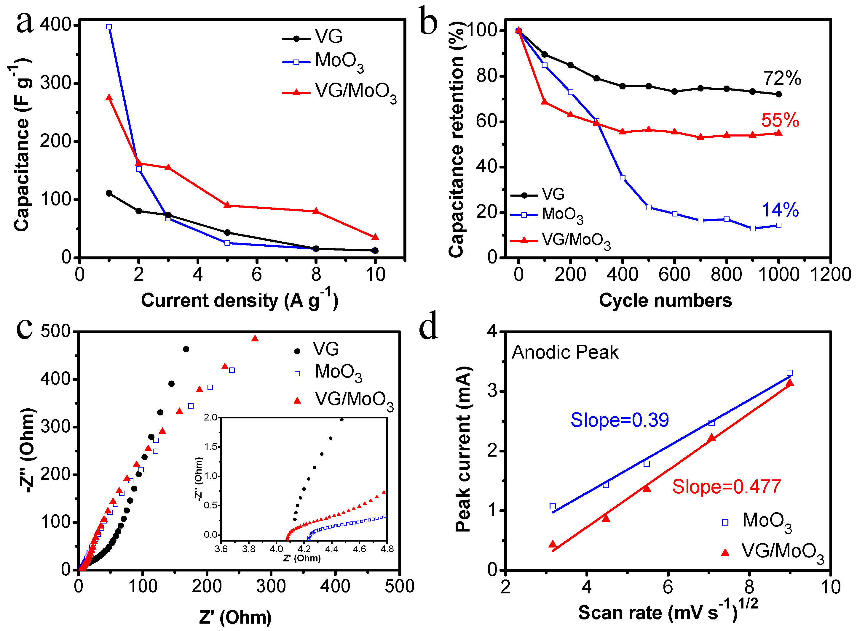
Figure 6d–f show the galvanostatic charge/discharge (GCD) properties of the three samples at different testing current densities. The discharging capacitance of the pristine VGs was measured as 110.8, 80.5, 73.8, 43.7, 16, and 12.5 F g
−1 with the working current densities of 1, 2, 3, 5, 8, and 10 A g
−1. Under these conditions, the discharging capacitance of the pristine MoO
3 nanosheets was 397.5, 152.7, 67.8, 25.6, 16, and 12.5 F g
−1. The specific rate performance of the samples is shown in
Figure 7a to make the comparison easier. Notably, the VGs possess small capacitance at low current densities, but exhibit no dramatic degradation with an increase in current density, demonstrating a high-rate performance (black curve in
Figure 7a). In contrast, the MoO
3 nanosheets have large initial capacitances but a faster decay (blue curve in
Figure 7a). The composite VG/MoO
3 nanosheets combine the advantages of the aforementioned two materials. Hence, this electrode material presented a discharging capacitance of 275, 162.5, 154.8, 90, 80, and 35 F g
−1 at different current densities of 1, 2, 3, 5, 8, and 10 A g
−1, exhibiting both an excellent energy storage capability and a high-rate performance (see
Figure 6f and red curve in
Figure 7a). Such an outstanding rate capability of the VG/MoO
3 sample is attributed to its unique VG transition layer structure, which provides plenty of high-conductivity paths for the transfer and diffusion of ions and electrons, and further improves the speed of electrochemical reactions.
The cycling capacitance retention rate is another important property for supercapacitors.
Figure 7b shows the cycling performance of the prepared samples, repeatedly charging/discharging for 1000 cycles at a current density of 2.0 A g
−1. The values of capacitance retention were recorded as 72%, 14%, and 55%, respectively, for the VG, MoO
3, and VG/MoO
3 samples. According to the electric-double-layer theory, the material structure or phase of the VG electrode did not change during the charging and discharging process, resulting in a preferable cycling stability. However, the capacitance retention of the pristine MoO
3 nanosheets decreased rapidly with an increase in the process of charging/discharging. This is because the volume and crystal structure of pseudo-capacitive materials are easy to change in repeated redox reactions, which impairs the stability of electrode materials. Based on this, in the proposed VG/MoO
3 nanosheets, the VG transition layer not only enhances the adhesion of MoO
3 nanosheets but also relieves the volume and structure changes of electrodes. Therefore, the VG/MoO
3 sample exhibited a better capacitance retention and cycling performance than the MoO
3 electrode.
Electrochemical impedance spectroscopy (EIS) properties were also tested to study the electrochemical kinetics of different samples (
Figure 7c). Typical Nyquist plots can be divided into two parts: the semicircle in high-frequency regions and the inclined line in low-frequency regions, commonly revealing the characteristics of interfacial resistance (
Ri), charge-transfer resistance (
Rct), and Warburg impedance (
Zw). Specifically,
Ri is obtained from the intercept of semicircular start point and horizontal axis and it denotes the total resistance of electrodes, electrolytes, current collectors, etc.
Rct represents the diameter of the semicircle, referring to the charge accumulation/release resistance on the surface of electrode. In this study, the VG/MoO
3 sample exhibited a relatively lower
Ri of 4.09 Ω compared with the MoO
3 sample (~4.25 Ω). This attributes to a reduced contact resistance with the assistance of VG transition layers between Ni foam and MoO
3 nanosheets. However, the pristine VGs exhibited a similar value of
Ri but a significant increase in
Rct compared with the other two materials, indicating difficult charge accumulation and release for pure graphene. In addition, the slope of inclined lines in
Figure 7c is represented as
Zw, which is related to the diffusion resistance inside the electrode. Herein, the pristine VGs show a steeper slope in low-frequency region, implying a fast diffusion of ions and electrons in the material. Unlike VGs, the other two samples reflect similar low-frequency characteristics and slopes. Therefore, we further studied the diffusion kinetic process of the MoO
3 and VG/MoO
3 samples by analyzing the CV curves (
Figure 6b,c) under different scanning rates. According to the Randles–Sevcik theory [
37,
38,
39], the anodic peak current (
ip) can be described as follows:
where
n is the number of transferring electrons in the process of charge/discharge reactions,
S is the effective contact area,
D is the diffusion coefficient,
C is the concentration of electrolyte, and
v is the scanning rate. Since the values of
n,
S, and
C are relatively constant, the anodic peak current (
ip) and the square root of the scanning rate (
v1/2) should have a linear relationship, in which the slope should be the diffusion coefficient (
D). As shown in
Figure 7d, the diffusion coefficient of the VG/MoO
3 nanosheets (~0.477) was calculated to be greater than that of the MoO
3 nanosheets (~0.39). The result indicates a rapid diffusion rate and superior rate capability of the composite nanomaterial, owing to the involvement of graphene carbon materials.
According to the above results, we believe that the energy storage performance of the proposed nano-scaled VG/MoO3 electrode should contain both behaviors of capacitive and diffusion-charging storage processes, which were controlled by the electric-double-layer capacitance mechanism (from VGs) and the pseudo-capacitance mechanism (from MoO3), respectively. With the speed of the scanning rate increasing, the capacitive behavior gradually becomes dominant. This is because the electrons and ions may have no time to diffuse to the deep layer of the electrode material for a reversible electrochemical reaction, which only occurs on the surface or near the surface of the material. Energy storage in such a case mainly depends on the adsorption of ions and electrons. Compared with MoO3, the VG/MoO3 nanosheets have smaller structural dimensions to increase the effective contact area, as well as lower charge transfer resistance and larger diffusion coefficient to accelerate ions and electrons transfer. Therefore, the VG/MoO3 electrode exhibits higher capacitive and diffusion-charging contributing behaviors at a high scanning rate.


 ,
, 