Article

Nanoindentation of Chromium Oxide Possessing Superior Hardness among Atomic-Layer-Deposited Oxides

Department of Materials Science, Institute of Physics, University of Tartu, W. Ostwald Str. 1, 50411 Tartu, Estonia
*
Author to whom correspondence should be addressed.
Nanomaterials 2022, 12(1), 82; https://doi.org/10.3390/nano12010082
Submission received: 24 November 2021 / Revised: 18 December 2021 / Accepted: 24 December 2021 / Published: 29 December 2021

Abstract

:
Chromium (III) oxide is a technologically interesting material with attractive chemical, catalytic, magnetic and mechanical properties. It can be produced by different chemical and physical methods, for instance, by metal–organic chemical vapor deposition, thermal decomposition of chromium nitrate Cr(NO3)3 or ammonium dichromate (NH4)2Cr2O7, magnetron sputtering and atomic layer deposition. The latter method was used in the current work to deposit Cr2O3 thin films with thicknesses from 28 to 400 nm at deposition temperatures from 330 to 465 °C. The phase composition, crystallite size, hardness and modulus of elasticity were measured. The deposited Cr2O3 thin films had different structures from X-ray amorphous to crystalline α-Cr2O3 (eskolaite) structures. The averaged hardness of the films on SiO2 glass substrate varied from 12 to 22 GPa and the moduli were in the range of 76–180 GPa, as determined by nanoindentation. Lower values included some influence from a softer deposition substrate. The results indicate that Cr2O3 could be a promising material as a mechanically protective thin film applicable, for instance, in micro-electromechanical devices.

1. Introduction

Chromium (III) oxide has been researched as a corrosion- and wear-resistant, mechanically protective hard coating, a component in glasses and glass ceramics, a cermet-type hard material or in other composites or as a sintering additive [1,2,3,4,5,6,7,8,9,10,11,12]. Some research has been focused on doped and pristine Cr2O3’s optical, magnetic, catalytic or sensory properties [13,14,15,16,17,18,19,20,21,22,23].
A number of different physical and chemical methods have been employed to produce Cr2O3 or the materials containing it. The physical techniques have included detonation and plasma spraying, different magnetron sputtering techniques and pulsed laser deposition [1,2,10,11,12,15,24]. The chemical techniques have included thermal decomposition of or co-precipitation from Cr(NO3)3∙9H2O, chemical vapor deposition (CVD) from CrCl3 and H2O at 900 °C or CrO3 and I2 at 500 °C, metal–organic chemical vapor deposition from Cr(CO)6, laser-assisted CVD from O2 and Cr(CO)6 and atomic layer deposition (ALD) from CrO2Cl2 and CH3OH precursors or from chromium acetyl acetonate and ozone [9,13,14,25,26,27,28,29].
Aside from the usual thin film deposition, some of the used techniques have resulted in various appearances of Cr2O3. For instance, the CVD from CrCl3 and H2O at 900 °C resulted in single crystalline Cr2O3 nanowires and nanobelts [14]. The decomposition of Cr(NO3)3 ∙ 9H2O, mixed with zirconia–toughened alumina at 600 °C, gave microparticles, whereas the co-precipitation from the same precursor resulted in nanoparticles [9,13]. CVD using CrO3 and I2 at 500 °C as precursors resulted in Cr2O3 flakes [21].
The previous reports have indicated the Cr2O3 thin films possess a high hardness of over 20 GPa [10,14,15,30,31,32]. In some conditions the processes produced chromia with lower hardness, even down to an 8–10 GPa level [14]. Reported values for the moduli range from 160 to about 290 GPa. The lower hardness and modulus values tend to appear in the amorphous chromia, but the crystalline counterparts have higher values [10,14,15]. It has been shown that Cr2O3, alloyed with other elements, could result in a super-hard material [10].
Compared to previously noted techniques, ALD allows to deposit conformal thin films on basically arbitrary three-dimensional shapes through the employment of the self-limiting irreversible and saturated surface reactions [33]. This feature makes ALD a very good tool to coat parts of micro-electromechanical devices or other systems to create surfaces with modified mechanical properties or, for instance, to act as a catalyst on a mesoporous substrate [34,35,36,37,38].
Even though Cr2O3 has been deposited before using ALD, the mechanical properties have not been reported [21,22]. The present work was dedicated to the investigation of the viability of atomic-layer-deposited Cr2O3 as a potentially hard and stiff material to be used as a mechanically protective or modifying thin film coating in micro- or nanoelectromechanical devices [31]. The crystallinity, the effect of the growth temperature and the thickness of the thin films were correlated to the nanoindentation hardness and modulus.

2. Experimental

The Cr2O3 thin films were deposited from CrO2Cl2 and CH3OH (Sigma-Aldrich, Darmstadt, Germany) in an in-house built atomic layer deposition reactor [39]. The detailed description and results can be found in previously published article [26]. Briefly, the films were grown on fused silica substrates at the growth temperature Tg of 330, 375, 420 and 465 °C. The cycle count was varied between 400–4300 ALD cycles. Each cycle consisted of 0.2 s exposure to CrO2Cl2, 2 s purge with dry N2, 2 s exposure to CH3OH vapors and another 2 s N2 purge. Both precursors were volatilized at −20 °C.
The crystallographic phase composition and the apparent crystallite size Dv were determined in direction of the normal to the lattice plane (104) by using Voigt decomposition analysis and SRM-660 (NIST, Gaithersburg, MD, USA) as reference material for diffraction peak instrumental broadening calibration [40]. Thickness of the films was determined using X-ray diffraction (XRD) and reflectivity (XRR) methods on diffractometer SmartLab™ (Rigaku, Tokyo, Japan) working at 8.1kW (Cu Kα radiation, λ = 0.154178 nm). Asymmetric 2θ-scan at fixed grazing incidence angle of ω = 0.42° (GIXRD) was used for phase composition analysis. In the GIXRD experiment, the Dv was determined in direction that is approximately 16.6° inclined to the sample surface normal. Texture coefficient of reflections (Thkl) was calculated from the following equation [41]: Thkl = IOBShkl/IDBhkl/<IOBS>, where IOBShkl is the observed absolute intensity of the reflection hkl; IDBhkl is the relative intensity of reference reflection hkl in the database; and <IOBS> is an average over all observed reflections of the ratio of observed to reference peak intensity values. Thkl is close to 1.0 for a randomly oriented polycrystalline sample and approaches to the number of observed reflections for a sample showing high preferred (hkl) orientation.
High-resolution scanning transmission electron microscopy (STEM) investigations were carried out by using a Titan Themis 200 microscope (FEI, Hillsboro, OR, USA) equipped with a Cs-probe corrector and operated at 200 kV. A sample for the STEM study in the form of thin cross-sectional lamella was prepared by a focused ion beam by using an in-situ lift-off technique in the scanning electron microscope Helios NanoLab 600 Dual Beam system (FEI, Hillsboro, OR, USA). Prior to the lamella preparation procedure, a platinum layer was deposited on the specimen by magnetron sputtering to minimize the charging of the specimen and to protect the chromium oxide film from the ion beam milling effect.
The hardness and elastic modulus of ALD Cr2O3 films were investigated by using nanoindentation device Bruker Hysitron Triboindenter TI 980 (Billerica, MA, USA; Minneapolis, MN, USA). The samples were measured in continuous stiffness mode by using a Berkovich-type diamond tip. The device was calibrated by using a fused quartz standard (Bruker) with defined hardness of 9.25 GPa and reduced modulus of 69.6 GPa. The overall arithmetic average of 17 measurements of the fused quartz was 9.18 GPa for hardness and 70.1 GPa for modulus. The strain rate of 0.05 nm/s and tip vibration frequency (220 Hz) were kept constant during the calibration and measurements. The calibrations were performed before and after measurements. The latter results indicated that the tip was still in good condition and assured the correctness of the measurements. The calibrations indicated that the valid displacement range was approximately from 20 nm to 100 nm. In the given range, the deposition substrate (SiO2 glass) had hardness of 8 ± 0.5 GPa and modulus of 61 ± 1.5 GPa (here, the error margins indicate the absolute minimum and maximum deviation at a given measurement point). The standard deviations of a single measurement remained near 3 GPa for modulus and 0.3 GPa for hardness at displacements around 20 nm. The deviations somewhat reduced towards higher displacements. Any single indentation measurement consisted of 61 data points in total, spread along the displacement range. The data points below displacements of 15 nm were removed. The data points near 20 nm of displacement were considered through analysis.
Due to the fact that some of the thin films were very thin in this study, the fused SiO2 glass made a good deposition substrate as it was free of any pile-up, sink-in or cracking effects which might occur during nanoindentation, possibly discrediting data analysis. Additionally, this is the reason for SiO2 glass usage as a calibration standard. As a glassy material, the substrate should have isotropic mechanical properties, which should avoid problems, such as film-induced cracking of a substrate [42].
Thirty separate continuous stiffness measurements were performed on each sample. Some low-quality measurements were removed, for instance, because of unsuitably high or unstable (thermal or positioning) drift rate of 0.29 nm/s, reducing the count of acceptable measurements by 5 in the worst case. Maximum drift level of 0.05 nm/s was the default acceptance level.

3. Results and Discussion

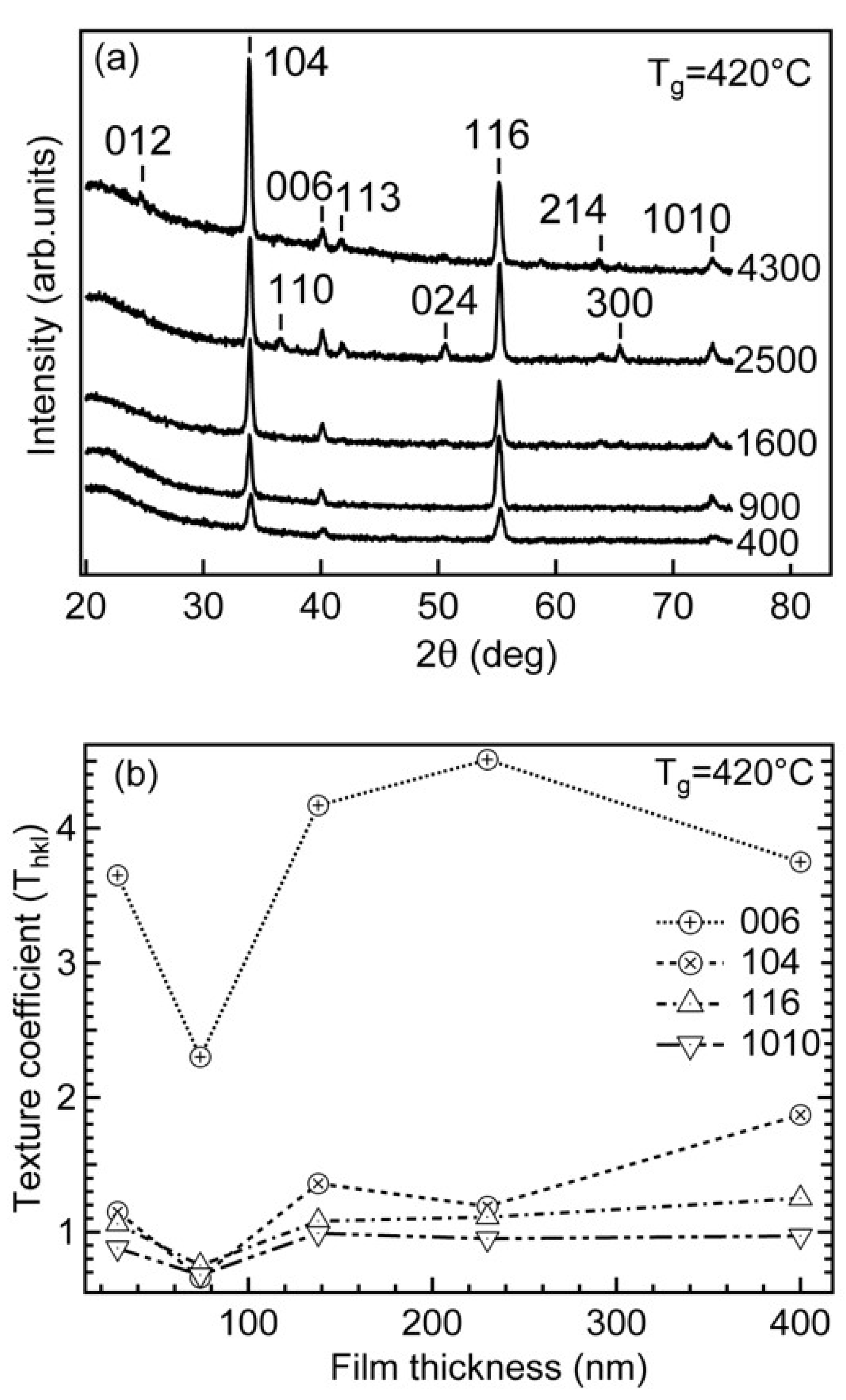
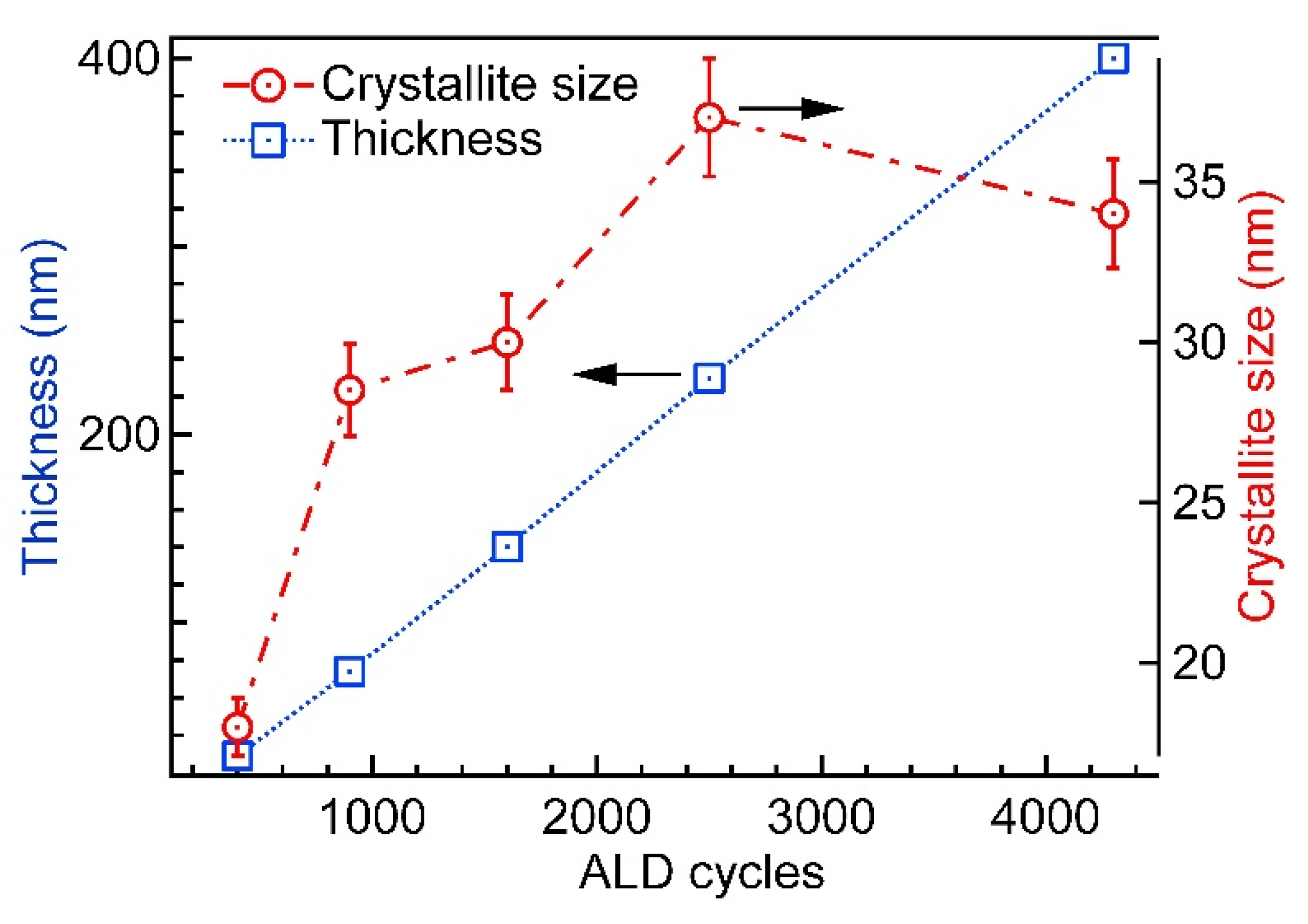
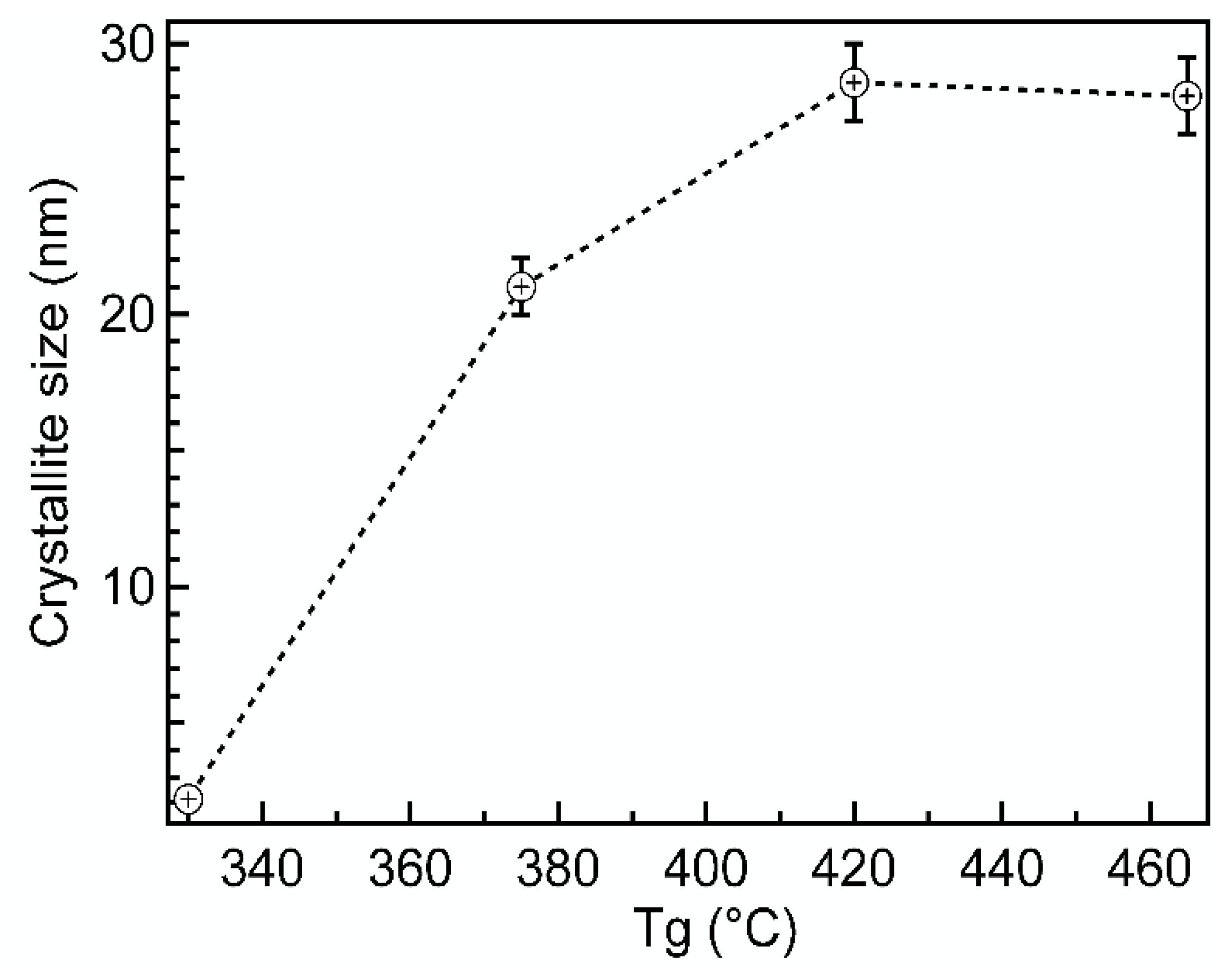
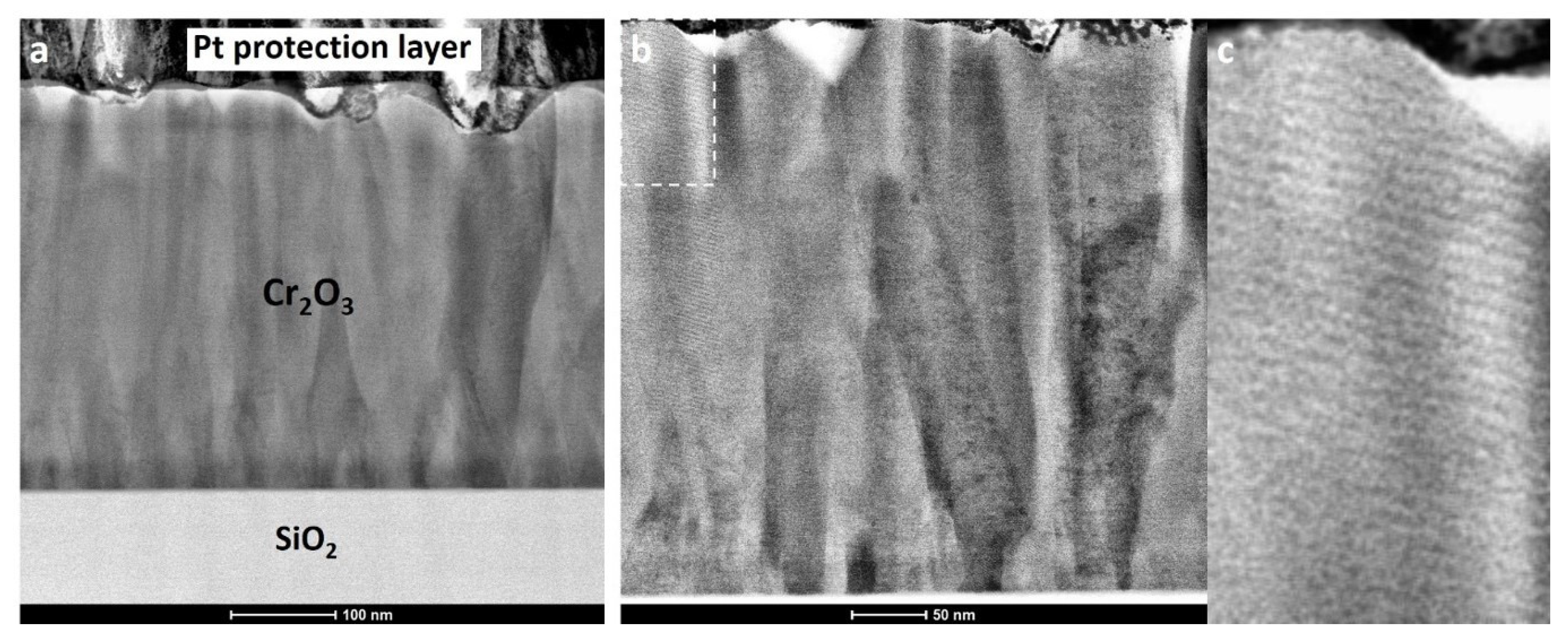
3.1. X-ray Diffraction

The crystallinity affects the (mechanical) properties of a material. Therefore, it is essential to measure the deposited thin film crystallographic properties, such as crystallinity and crystallite size.
Figure 1 shows that the crystallinity increased with the increase of the growth temperature Tg. The sample deposited at 330 °C was X-ray amorphous, but the samples deposited at higher temperatures showed reflections that were identified as belonging to α-Cr2O3 (mineral eskolaite, ICDD PDF-2 file number 01-078-5435).
The diffractograms of thin films with different cycle counts are shown in Figure 2.
Figure 2b shows the variation of texture coefficient Thkl for the dominating reflections (104), (006), (116) and (1010) as a function of the film thickness. The value of Thkl for the reflection 006 was a few times higher compared to the values for the other reflections. Pang et al. showed that the mechanical properties of Cr2O3 films change with the texture [30]. For instance, a film with strong (300) texture had hardness of about 28 GPa but was reduced to 20 GPa for a low-textured film. Similar results were gained by Luo et al. [15].
Considering that, in the GIXRD analysis, these observed reflections were generated from lattice planes that were inclined to the sample surface in the angle range of 20–38° and, by assuming modest mosaicity of the film, it can be concluded that the preferred growth direction of the films was close to the crystallographic [001] direction. The mosaicity of the films was determined and the preferred growth plane characterized in more detail also by symmetrical θ/2θ and in-plane XRD analysis for the two thickest samples (230 and 400 nm) that allowed to record diffraction reflections with acceptable signal-to-noise ratio for both of the analysis modes.
The θ/2θ-XRD pattern of the film deposited with 2500 cycles showed (bottom curve in Figure 3) two strong reflections (104 and 1010) and four weak reflections (006, 113, 116, 122), whereas the IP-XRD pattern exhibited two stronger reflections from the (104) and (110) lattice planes and weaker reflections from the (113), (202), (116), (214) and (300) planes. The appearance of the θ/2θ-reflection from the plane (104) and IP reflection from plane (110) are a clear indication that the preferred growth of this film was in the (104) plane or in the plane where the inclination angle relative to (104) plane was small. The high value of the full width of the half maximum (FWHM) of the 1010 reflection (∆ω = 51°) suggests that the mosaicity of this film was very high and the preferred growth direction varied approximately from −25 to +25° relative to the surface normal of the (104) plane. The refinement of the cell parameters determined from the IP and θ/2θ-XRD patterns and calculation of the lattice strain, relative to the parameters from the database (ICDD PDF-2), showed that the crystal lattice was slightly compressed (0.05–0.1%) in the direction of the surface normal and stretched approximately parallel to the surface by the same amount.
The IP and θ/2θ-XRD patterns from the film deposited with 4300 cycles showed (Figure 3) that, beside the (104) plane, the (001) plane appeared as a preferred growth plane. A relatively high intensity of the 006 reflection, the appearance of the 0012 reflection on the θ/2θ-XRD pattern, the two times smaller FWHM of the rocking curve of the 1010 reflection and the approximately 2.5–3 times larger values of the lattice strain (compared to the film deposited with 2500 cycles), but also strong 110 and 300 reflections on the IP-XRD patterns of this film, allowed us to conclude that, in thicker films (above 230 nm), the mosaicity decrease is accompanied by a preferred growth in the (001) plane.
The results of the film thicknesses deposited at 420 °C and the respective crystallite sizes are presented in Figure 4. The thickness measurement error for the thickest film was around 10 nm and for thinner films (below 100 nm) from 1 to 3 nm, reducing in coherence with the film thickness.
The growth rate of Cr2O3 at 420 °C, calculated from the slope of the film thickness in variation with ALD cycles, was 0.096 nm/cycle (determination coefficient R2 = 0.99). The linear correlation of the cycle count and resultant thin film thickness are characteristic of ALD.
It can be seen that the apparent crystallite size (Dv) depended remarkably on the number of growth cycles or, in other words, on film thickness. The crystallites grew fast during the first 900 cycles of deposition, reaching the size of about 30 nm. The further increase of crystallites proceeded considerably slower—within the next 1300 cycles the increase was only about 7 nm.
The deposition temperature Tg was also an important factor that controlled the crystallite size of Cr2O3. Figure 5 shows that Dv increased fast with the increase of Tg from 330 to 375 °C. Starting from Tg = 380 °C, the increase slowed down and saturated finally at 420 °C, reaching the maximum value of about 27–30 nm.
Khojieri et al. deposited at room temperature approximately 80 nm thick films of Cr2O3 on monocrystalline silicon by using DC magnetron sputtering [29]. Annealing a sample at 400 °C resulted in grain sizes approximately 28–31 nm, which is comparable to current work results.
The deposition conditions and the respective apparent crystallite size, film thickness and other results, determined by X-ray measurements, are gathered in Table 1. The integral width β of a reflection was the parameter that was used for calculation of crystallite size. Here it is presented for (104) reflection. Respective values can be seen in Table 1, which correspond to apparent X-ray crystallite size of 20–30 nm. The unit cell parameters compare well to database values.

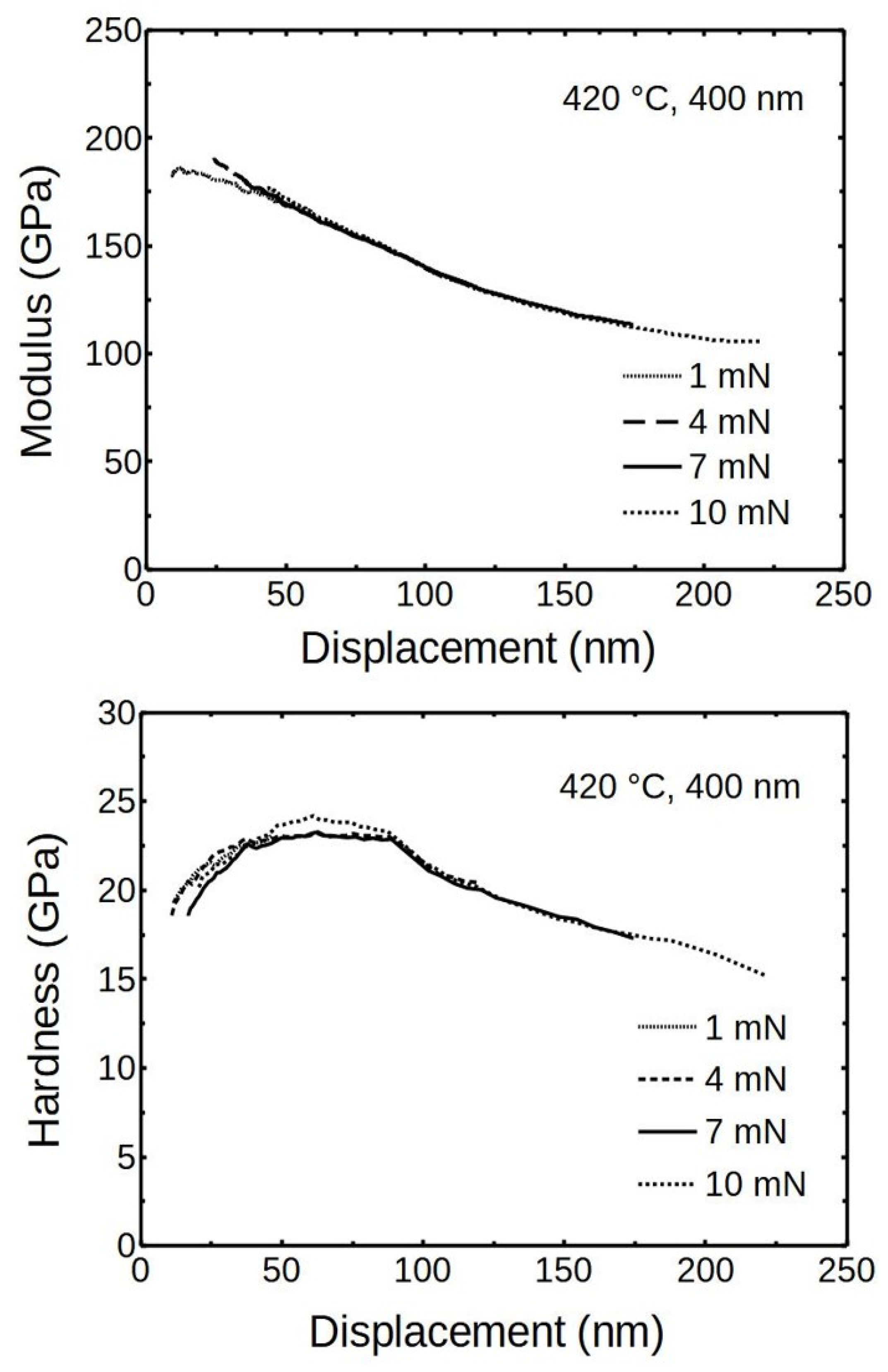
3.2. Nanoindentation

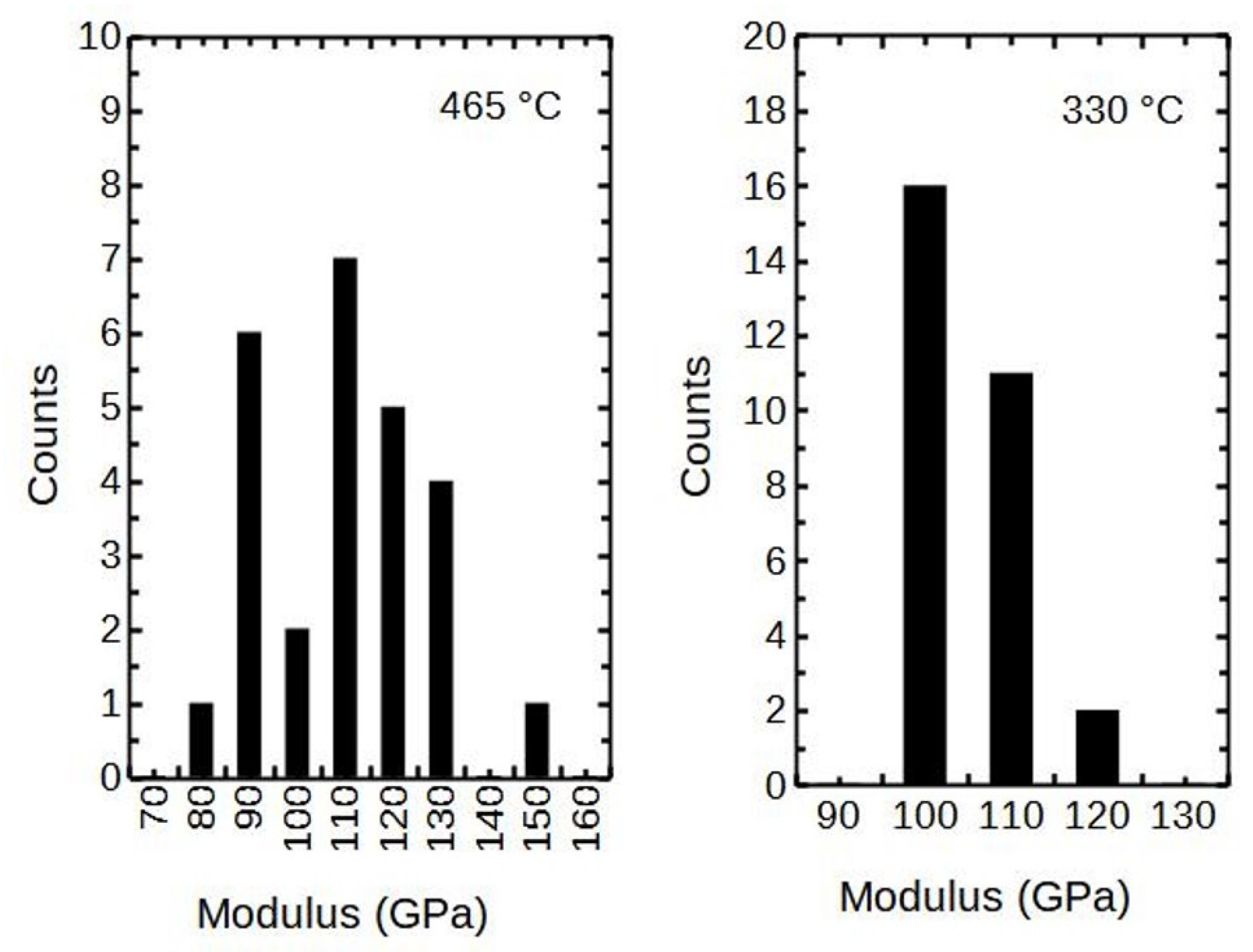
3.2.1. Relation of Hardness and Modulus to the Deposition Temperature

The relation of the deposition temperature Tg and the averaged reduced moduli of the films with thicknesses of 68–85 nm is shown in Figure 6. It can be seen that there was some dependence of moduli on Tg, but the difference was low—about 10 GPa (~10%) in between X-ray amorphous and crystalline thin films at the displacement of 20 nm. A likely reason for such low differences was the influence of a softer SiO2 substrate. Considering that the thin films had thicknesses of only about 68–85 nm, at the displacements of 20 nm, the substrate reduced the measured values and the differences thereof.
The differences in the averaged hardness values were within 15% (Figure 6). The higher values corresponded to the films with the appearance of the crystalline Cr2O3.
Pang et al. showed that the hardness and modulus of chromia thin film do increase with the increase in crystallinity [28]. They used reactive magnetron sputtering to produce Cr2O3 films and measured the range of hardness to be 11–21 GPa and 170–234 GPa for modulus, depending on the crystallinity. Khojier et al. measured the hardness of DC magnetron sputtered and annealed at 300 °C and 400 °C samples to be around 17–21 GPa and the respective moduli around 160–185 GPa [29].
The scattering of the nanoindentation results taken at 20 nm of displacement are presented in the histograms (Figure 7). It can be seen that the X-ray amorphous thin film deposited at 330 °C had lower scattering (±10 GPa) than the crystalline counterpart (±35 GPa) deposited at 465 °C. As an overall notice, the scatter widened with the growth temperature Tg.

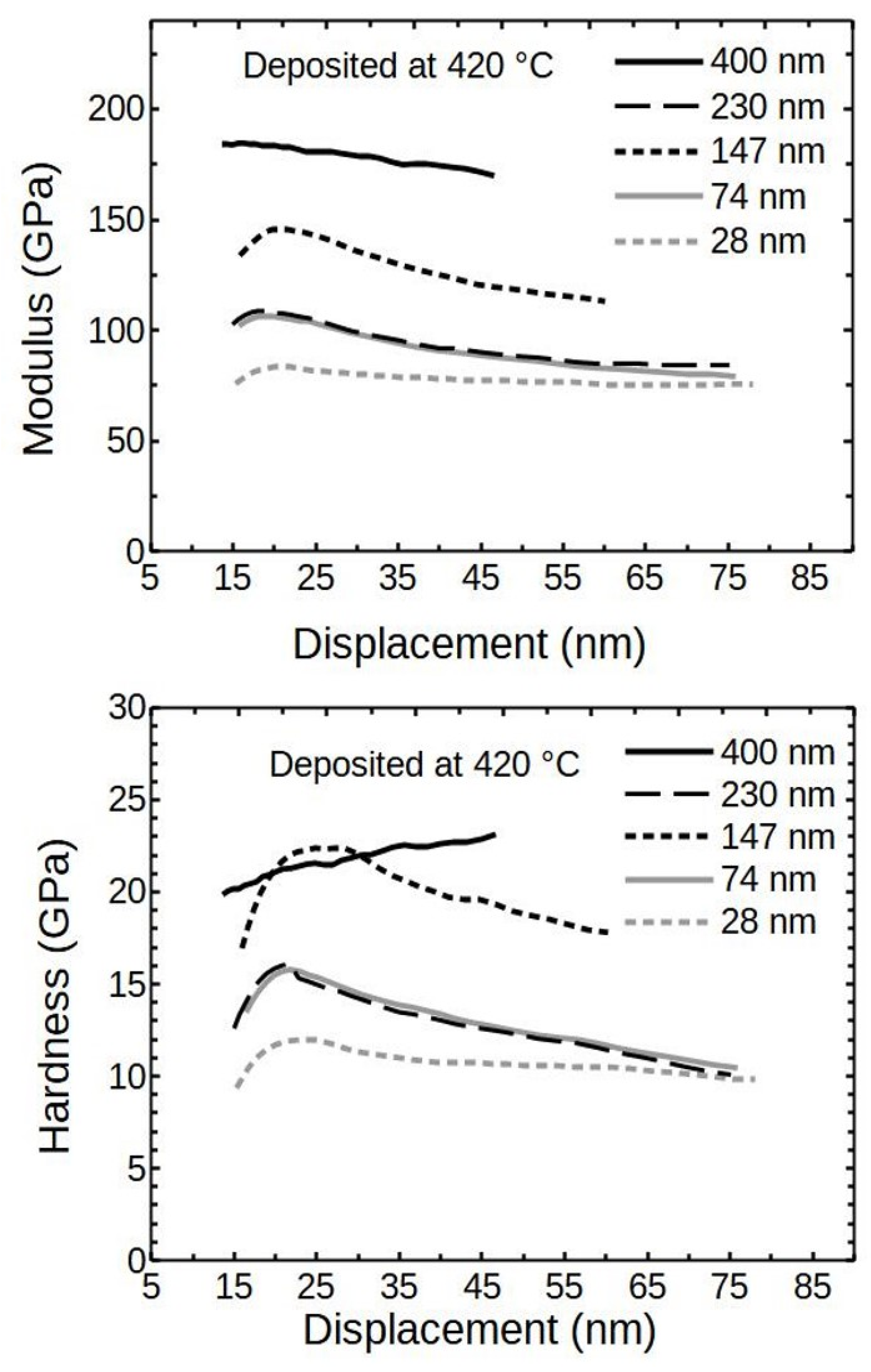
3.2.2. Relation between Hardness, Modulus and Thickness of Chromia

Figure 8 visualizes the relation between the modulus and the deposited thin film thickness (deposited at 420 °C). It indicates that the softer substrate has a reducing impact on the results, which diminished inversely with film thickness. The hardness showed similar trends as the moduli (Figure 8).
It can be seen that the hardness and modulus of the 230 nm thick sample had considerably lower values than 147 or 400 nm films. A logical expectation would be for the result to be positioned in between 147 and 400 nm thick samples. The detrimental effect was likely caused by the increased mosaicity and the presence of differently oriented crystallites, as shown in the XRD analysis.
The reducing effect caused by the substrate was not confirmed for the 400 nm thick film and the hardness seemed to increase perpetually. Therefore, the sample was investigated further. The second reason for a more in-depth search was an attempt to find the properties corresponding solely to the ALD Cr2O3 thin film.
The triboindenter was recalibrated to a displacement upper limit of about 300 nm because the indentation depths were expected to exceed the 100 nm limit of initial calibration. The using of maximum indentation forces of 4, 7 and 10 mN revealed that the results behaved at higher displacements, as expected, clearly showing the substrate influence (Figure 9).
Figure 9 indicates that the averaged measurements point at the modulus of elasticity of ALD Cr2O3 was around 200 ± 20 GPa. This compares well with the results published by Pang and Khojier, but it is about 80 GPa less than in Saeki’s work [26,27]. Saeki et al. calculated and measured at room temperature the modulus of elasticity of α-Cr2O3 to be 286 GPa. First-principles calculations indicated the bulk modulus of Cr2O3 to be around 240 GPa at 300 K, which is quite close to current results [43].
The averaged results for hardness at different loads gave similar curves, overlapping and showing a “plateau” at the displacement range of 30–80 nm, where the hardness was around 22.5 ± 1 GPa (Figure 9). The initial increasing hardness values, seen in measurements done on 400 nm film by using 1 mN, can be viewed as just the lead to the plateau.
The averaged modulus of 200 GPa and hardness of 22.5 GPa are characteristics of the ALD Cr2O3 thin film deposited at given conditions. It had a remarkably high hardness compared to the values previously reported for oxide thin films deposited by ALD. In most cases, the reported values were below 15 GPa [44,45,46,47]. Although the hardness here did not reach the super-hardness level of 40 GPa, the 22 GPa would be a good starting point to develop super-hard ALD Cr2O3-based films [10].
The summarized results of XRD and nanoindentation of current work are gathered in Table 2.
It is clear from Table 2 that the sample with 2500 deposition cycles had markedly lower hardness and modulus compared to samples with 1600 and 4300 cycles. This could be attributed to the different crystallite orientations, as was seen from XRD (Figure 2). Crystallite orientation is known to have influence on material properties [12,48]. On the other hand, the determined XRD apparent crystallite sizes did not correlate well with respective hardnesses or moduli. The hardness value for 230 nm thick film was considerably lower than for neighboring samples, even though the crystallites had fairly similar sizes. The lower hardness could not be attributed to intrinsic stresses as the unit cell parameters in Table 1 did not indicate any remarkable stresses.
The Cr2O3 film deposited at 420 °C with 4300 ALD cycles was also studied using scanning transmission electron microscopy. Figure 10a shows a cross-sectional bright-field STEM image of the Cr2O3 film on SiO2 substrate with a platinum protection layer on top. Due to the lower atomic number, the SiO2 substrate appears significantly brighter compared to the Cr2O3 film on the image. The image shows continuous dense Cr2O3 with no gaps or voids between various nucleated grains, which indicates a complete coalescence of the nucleation islands. The thickness of the film is relatively uniform, but some surface roughness is present. The source of the surface roughness might be a result of the formation of quite large crystallites. The thickness of the film measured on the STEM image is around 400 nm, which is in agreement with the values obtained by the XRR studies.
As can be seen by the more uniform contrast, as well as the large areas with uniform Moiré fringes (Figure 10b,c) closer to the surface of the film, the size of the grains perpendicular to the substrate tended to increase with film thickness. The increase in the lateral size of the favorably oriented grains led to the impairment of the growth of other grains and a decrease of mosaicity of the film.
Similar columnar structures were reported previously in the case of magnetron sputtered Cr2O3, but the authors did not discuss the relationship between mechanical properties and crystallite size, film thickness or the columnar microstructure [10,24]. It seems that, at the half height in the STEM image, there is a change in crystallite nucleation site count and the crystallites seem to start coalescing. This kind of growth kinetics change can introduce local mechanical stresses which, again, could initiate phase changes in a material to relieve the stress. Considering that the alpha form of Cr2O3 is a stable polymorph, the possible phase change is unlikely. On the other hand, it cannot be ruled out that residual stress somewhat changes the crystallite orientations or positioning and this could occur ex situ, over a period of time. An additional 70% thickness increase (from 230 nm to 400 nm) could, again, stabilize the structure enough that any probable changes, such as increased mosaicity, are hindered. This could be the reason why the XRD results and mechanical properties are different for Cr2O3 thin films with thicknesses of 230 and 400 nm. Unfortunately, the current set-up was to characterize the thin films ex situ and not in situ. The latter could be considered for next experiments to get more insight. Abadis et al. published a comprehensive review on stresses in thin films and related effects, including phase changes, detrimental effect on mechanical properties and so on [49].

4. Conclusions

The study suggests that ALD Cr2O3 is hard and relatively stiff but, in some cases, the uniform mechanical behavior might be hard to achieve. It can be concluded that the X-ray amorphous ALD Cr2O3 had the lowest dispersion of hardness and modulus, but the averaged values remained lower as compared to crystalline samples. Higher crystallinity in thin films results in higher hardness and modulus but also the higher scatter of the results, which has to be considered in applications. The optimization of deposition conditions could help to gain an ALD Cr2O3 thin film with a lower dispersion of properties.
The research showed correlation between ALD conditions, such as growth temperature, and resulting mechanical properties, such as hardness, which can be taken as a guide in application or further research. The measurements showed that the averaged hardness was 22.5 ± 1 GPa and the modulus was 200 ± 25 GPa for the film deposited at 420 °C. The hardness of thin films indicates that it could be used as starting point for developing super-hard ALD coatings.
Atomic-layer-deposited Cr2O3 looks like a very good candidate material as a mechanically protective coating. The Cr2O3 coating would considerably enhance the surface properties of, for instance, the silicon- or silicon-oxide-based parts of micromechanical devices. Due to the conformal growth of ALD thin films, these could be applied on basically arbitrary shapes, which is very convenient in the case of micro-electromechanical systems. The actual performance, naturally, depends on the selected substrate, thin film thickness and deposition conditions (i.e., the temperature).

Author Contributions

Conceptualization, data curation, project administration, T.J.; formal analysis, T.J. and H.M.; investigation, T.J. and A.T. (Aivar Tarre); writing original draft, T.J., H.M. and J.K.; writing—review and editing, A.T. (Aivar Tarre) and A.T. (Aile Tamm); funding acquisition and resources, A.T. (Aile Tamm). All authors have read and agreed to the published version of the manuscript.

Funding

This work was funded by the European Regional Development Fund project TK134 “Emerging orders in quantum and nanomaterials”, Estonian Research Agency project PRG4 “Emerging novel phases in strongly frustrated quantum magnets” and Estonian Research Agency project PRG753.

Institutional Review Board Statement

Not applicable.

Informed Consent Statement

Not applicable.

Data Availability Statement

The data presented in this study are available on request from the corresponding author.

Acknowledgments

This work was supported by the ERDF project Centre of Technologies and Investigations of Nanomaterials (NAMUR+, project number 2014-2020.4.01.16-0123).

Conflicts of Interest

The authors declare no conflict of interest.

References

  1. Tang, J.-F.; Huang, C.-H.; Lin, C.-Y.; Tsai, Y.-J.; Chang, C.-L. Effect of plasma nitriding and modulation structure on the adhesion and corrosion resistance of CrN/Cr2O3 coatings. Surf. Coat. Technol. 2019, 379, 125051. [Google Scholar] [CrossRef]
  2. Babu, P.S.; Sen, D.; Jyothirmayi, A.; Krishna, L.R.; Rao, D.S. Influence of microstructure on the wear and corrosion behavior of detonation sprayed Cr2O3-Al2O3 and plasma sprayed Cr2O3 coatings. Ceram. Int. 2018, 44, 2351–2357. [Google Scholar] [CrossRef]
  3. Yıldız, B.K.; Tür, Y.K. An investigation of equibiaxial flexural strength and hardness properties of Al2O3–Ni nanocomposites-based microstructures with ZrO2 and Cr2O3 additives. Mat. Sci. Eng. A 2019, 758, 103–111. [Google Scholar] [CrossRef]
  4. Yıldız, B.K.; Yılmaz, H.; Tür, Y.K. Evaluation of mechanical properties of Al2O3–Cr2O3 ceramic system prepared in different Cr2O3 ratios for ceramic armour components. Ceram. Int. 2019, 45, 20575–20582. [Google Scholar] [CrossRef]
  5. Norfauzi, T.; Hadzley, A.B.; Azlan, U.A.A.; Afuza, A.A.; Faiz, M.M.; Naim, M.F. Fabrication and machining performance of ceramic cutting tool based on the Al2O3-ZrO2-Cr2O3 compositions. J. Mater. Res. Technol. 2019, 8, 5114–5123. [Google Scholar] [CrossRef]
  6. He, X.; Li, C.; Liu, J.; Huang, Q.; Shen, X.; Liu, T.; Lu, A. Glass forming ability, structure and properties of Cr2O3–Fe2O3 co-doped MgO–Al2O3–SiO2–B2O3 glasses and glass-ceramics. J. Non-Cryst. Solids 2020, 529, 119779. [Google Scholar] [CrossRef]
  7. Manshor, H.; Abdullah, E.C.; Azhar, A.Z.A.; Sing, Y.W.; Ahmad, Z.A. Microwave sintering of zirconia-toughened alumina (ZTA)-TiO2-Cr2O3 ceramic composite: The effects on microstructure and properties. J. Alloys Compd. 2017, 722, 458–466. [Google Scholar] [CrossRef]
  8. Khodaei, M.; Yaghobizadeh, O.; Baharvandi, H.R.; Esmaeeli, S.; Javi, H. The effect of Cr2O3 additions on sinterability and mechanical properties of liquid-phase sintered SiC ceramics. J. Alloys Compd. 2020, 829, 154501. [Google Scholar] [CrossRef]
  9. Xia, J.F.; Nian, H.Q.; Liu, W.; Wang, X.G.; Jiang, D.Y. Effect of Cr2O3 derived from Cr(NO3)3·9H2O precursor on the densification and mechanical properties of zirconia-toughened alumina (ZTA) composites. Ceram. Int. 2016, 42, 9116–9124. [Google Scholar] [CrossRef]
  10. Mohammadtaheri, M.; Li, Y.; Corona-Gomez, J.; Yang, Q. An investigation on synthesis and characterization of superhard Cr-Zr-O coatings. Surf. Coat. Technol. 2019, 375, 694–700. [Google Scholar] [CrossRef]
  11. Yang, X.; Dong, S.; Zeng, J.; Zhou, X.; Jiang, J.; Deng, L.; Cao, X. Sliding wear characteristics of plasma-sprayed Cr2O3 coatings with incorporation of metals and ceramics. Ceram. Int. 2019, 45, 20243–20250. [Google Scholar] [CrossRef]
  12. Pedersen, K.; Bøttiger, J.; Sridharan, M.; Sillassen, M.; Eklund, P. Texture and microstructure of Cr2O3 and (Cr,Al)2O3 thin films deposited by reactive inductively coupled plasma magnetron sputtering. Thin Solid Film. 2010, 518, 4294–4298. [Google Scholar] [CrossRef] [Green Version]
  13. Carta, G.; Natali, M.; Rossetto, G.; Zanella, P.; Salmaso, G.; Restello, S.; Rigato, V.; Kaciulis, S.; Mezzi, A. A Comparative Study of Cr2O3 Thin Films Obtained by MOCVD using Three Different Precursors. Chem. Vap. Depos. 2005, 11, 375–380. [Google Scholar] [CrossRef]
  14. Kao, A.S.; Doerner, M.F.; Novotny, V.J. Processing effects on the tribological characteristics of reactively sputtered chromium oxide (Cr2O3) overcoat films. J. Appl. Phys. 1989, 66, 5315–5321. [Google Scholar] [CrossRef]
  15. Luo, F.; Pang, X.; Gao, K.; Yang, H.; Wang, Y. Role of deposition parameters on microstructure and mechanical properties of chromium oxide coatings. Surf. Coat. Technol. 2007, 202, 58–62. [Google Scholar] [CrossRef]
  16. Singh, J.; Verma, V.; Kumar, R. Preparation and structural, optical studies of Al substituted chromium oxide (Cr2O3) nanoparticles. Vacuum 2019, 159, 282–286. [Google Scholar] [CrossRef]
  17. Yang, S.; Liu, S.; Lan, C.; Yang, S. Single crystalline Cr2O3 nanowires/nanobelts: CrCl3 assistant synthesis and novel magnetic properties. Appl. Surf. Sci. 2012, 258, 8965–8969. [Google Scholar] [CrossRef]
  18. Baraskar, P.; Chouhan, R.; Agrawal, A.; Choudhary, R.J.; Sen, P. Weak ferromagnetism at room temperature in Ti incorporated Cr2O3 thin film. Phys. B Condens. Matter 2019, 571, 36–40. [Google Scholar] [CrossRef]
  19. Nadeem, K.; Kamran, M.; Javed, A.; Zeb, F.; Hussain, S.S.; Mumtaz, M.; Krenn, H.; Szabo, D.V.; Brossmann, U.; Mu, X. Role of surface spins on magnetization of Cr2O3 coated γ-Fe2O3 nanoparticles. Solid State Sci. 2018, 83, 43–48. [Google Scholar] [CrossRef]
  20. Yang, T.H.; Mal, S.; Jin, C.; Narayan, R.J.; Narayan, J. Epitaxial VO2/Cr2O3/sapphire heterostructure for multifunctional applications. Appl. Phys. Lett. 2011, 98, 022105201. [Google Scholar] [CrossRef]
  21. Mu, S.; Belashchenko, K.D. Influence of strain and chemical substitution on the magnetic anisotropy of antiferromagnetic Cr2O3: An ab-initio study. Phys. Rev. Mater. 2019, 3, 034405. [Google Scholar] [CrossRef]
  22. Asghari, S.; Haghighi, M.; Taghavinezhad, P. Plasma-enhanced scattering of Cr2O3 over ceria-doped MCM-41 nanostructured catalyst used in CO2 oxidative dehydrogenation of ethane to ethylene. Microporous Mesoporous Mater. 2019, 279, 165–177. [Google Scholar] [CrossRef]
  23. Kim, T.H.; Yoon, J.W.; Kang, Y.C.; Abdel-Hady, F.; Wazzan, A.A.; Lee, J.H. A strategy for ultrasensitive and selective detection of methylamine using p-type Cr2O3: Morphological design of sensing materials, control of charge carrier concentrations, and configurational tuning of Au catalysts. Sens. Actuators B Chem. 2017, 240, 1049–1057. [Google Scholar] [CrossRef]
  24. Mohammadtaheri, M.; Yang, Q.; Li, Y.; Corona-Gomez, J. The Effect of Deposition Parameters on the Mechanical Properties of Chromium Oxide Coatings Deposited by Reactive Magnetron Sputtering. Coatings 2018, 8, 111. [Google Scholar] [CrossRef] [Green Version]
  25. Hafeez, M.; Saleemi, A.S.; Rehman, S.U.; Adrees, M.; Mehmood, S.; Mir, I.A.; Zhu, L. CVD growth of layered Cr2O3 hexagonal flakes for optoelectronic applications. Appl. Surf. Sci. 2021, 536, 147713. [Google Scholar] [CrossRef]
  26. Tarre, A.; Aarik, J.; Mändar, H.; Niilisk, A.; Pärna, R.; Rammula, R.; Uustare, T.; Rosental, A.; Sammelselg, V. Atomic layer deposition of Cr2O3 thin films: Effect of crystallization on growth and properties. Appl. Surf. Sci. 2008, 254, 5149–5156. [Google Scholar] [CrossRef]
  27. Sammelselg, V.; Tarre, A.; Lu, J.; Aarik, J.; Niilisk, A.; Uustare, T.; Netšipailo, I.; Rammula, R.; Pärna, R.; Rosental, A. Structural characterization of TiO2-Cr2O3 nanolaminates grown by atomic layer deposition. Surf. Coat. Technol. 2010, 204, 2015–2018. [Google Scholar] [CrossRef]
  28. Tripathi, T.S.; Niemelä, J.P.; Karppinen, M. Atomic layer deposition of transparent semiconducting oxide CuCrO2 thin films. J. Mater. Chem. C 2015, 3, 8364–8371. [Google Scholar] [CrossRef] [Green Version]
  29. Sousa, P.M.; Silvestre, A.J.; Conde, O. Cr2O3 thin films grown at room temperature by low pressure laser chemical vapour deposition. Thin Solid Film. 2011, 519, 3653–3657. [Google Scholar] [CrossRef] [Green Version]
  30. Pang, X.; Gao, K.; Volinsky, A.A. Microstructure and mechanical properties of chromium oxide coatings. J. Mater. Res. 2007, 22, 3531–3537. [Google Scholar] [CrossRef] [Green Version]
  31. Khojier, K.; Savaloni, H.; Ashkabusi, Z.; Dehnavi, N.Z. Structural, mechanical and tribological characterization of chromium oxide thin films prepared by post-annealing of Cr thin films. Appl. Surf. Sci. 2013, 284, 489–496. [Google Scholar] [CrossRef]
  32. Saeki, I.; Ohno, T.; Seto, D.; Sakai, O.; Sugiyama, Y.; Sato, T.; Yamauchi, A.; Kurokawa, K.; Takeda, M.; Onishi, T. Measurement of Young’s modulus of oxides at high temperature related to the oxidation study. Mater. High Temp. 2014, 28, 264–268. [Google Scholar] [CrossRef]
  33. Miikkulainen, V.; Leskelä, M.; Ritala, M.; Puurunen, R.L. Crystallinity of inorganic films grown by atomic layer deposition: Overview and general trends. J. Appl. Phys. 2013, 113, 021301. [Google Scholar] [CrossRef]
  34. Węgrzyniak, A.; Jarczewski, S.; Wach, A.; Hędrzak, E.; Kuśtrowski, P.; Michorczyk, P. Catalytic behaviour of chromium oxide supported on CMK-3 carbon replica in the dehydrogenation propane to propene. Appl. Catal. A Gen. 2015, 508, 1–9. [Google Scholar] [CrossRef]
  35. Brytavskyi, I.; Hušeková, K.; Myndrul, V.; Pavlenko, M.; Coy, E.; Zaleski, K.; Gregušová, D.; Yate, L.; Smyntyna, V.; Iatsunskyi, I. Effect of porous silicon substrate on structural, mechanical and optical properties of MOCVD and ALD ruthenium oxide nanolayers. Appl. Surf. Sci. 2019, 471, 686–693. [Google Scholar] [CrossRef]
  36. Jõgiaas, T.; Arroval, T.; Kollo, L.; Kozlova, J.; Käämbre, T.; Mändar, H.; Tamm, A.; Hussainova, I.; Kukli, K. Atomic layer deposition of alumina on gamma-Al2O3 nanofibres. Phys. Status Solidi 2014, 211, 403–408. [Google Scholar] [CrossRef]
  37. Jõgiaas, T.; Kollo, L.; Kozlova, J.; Tamm, A.; Hussainova, I.; Kukli, K. Effect of atomic layer deposited aluminium oxide on mechanical properties of porous silicon carbide. Ceram. Int. 2015, 41, 7519–7528. [Google Scholar] [CrossRef]
  38. Tripp, M.K.; Stampfer, C.; Miller, D.C.; Helbling, T.; Herrmann, C.F.; Hierold, C.; Gall, K.; George, S.M.; Bright, V.M. The mechanical properties of atomic layer deposited alumina for use in micro- and nano-electromechanical systems. Sens. Actuators A Phys. 2006, 130–131, 419–429. [Google Scholar] [CrossRef]
  39. Niilisk, A.; Rosental, A.; Gerst, A.; Sammelselg, V.; Uustare, T. Atomic-scale optical monitoring of initial growth of TiO2 thin films. In Smart Optical Inorganic Structures and Devices; International Society for Optics and Photonics: Bellingham, WA, USA, 2001; Volume 4318. [Google Scholar] [CrossRef]
  40. Mändar, H.; Felsche, J.; Mikli, V.; Vajakas, T. AXES1.9: New tools for estimation of crystallite size and shape by Williamson-Hall analysis. J. Appl. Cryst. 1999, 32, 345–350. [Google Scholar] [CrossRef]
  41. Barrett, C.S.; Massalski, T.B. Structure of Metals. In Crystallographic Methods, Principles and Data (International Series on Materials Science and Technology), 3rd ed.; Pergamon Press: Oxford, UK, 1980; p. 204. ISBN 978-0080261720. [Google Scholar]
  42. Guo, T.; Chen, Y.; Cao, R.; Pang, X.; He, J.; Qiao, L. Cleavage cracking of ductile-metal substrates induced by brittle coating fracture. Acta Mater. 2018, 152, 77–85. [Google Scholar] [CrossRef]
  43. Wang, Y.; Fang, H.; Zacherl, C.L.; Mei, Z.; Shang, S.; Chen, L.Q.; Jablonski, P.D.; Liu, Z.K. First-principles lattice dynamics, thermodynamics, and elasticity of Cr2O3. Surf. Sci. 2012, 606, 1422–1425. [Google Scholar] [CrossRef]
  44. Jõgiaas, T.; Zabels, R.; Tamm, A.; Merisalu, M.; Hussainova, I.; Heikkilä, M.; Maendar, H.; Kukli, K.; Ritala, M.; Leskelä, M. Mechanical properties of aluminum, zirconium, hafnium and tantalum oxides and their nanolaminates grown by atomic layer deposition. Surf. Coat. Technol. 2015, 282, 36–42. [Google Scholar] [CrossRef]
  45. Jõgiaas, T.; Zabels, R.; Tarre, A.; Tamm, A. Hardness and modulus of elasticity of atomic layer deposited Al2O3-ZrO2 nanolaminates and mixtures. Mater. Chem. Phys. 2020, 240, 122270. [Google Scholar] [CrossRef]
  46. Berdova, M.; Liu, X.; Wiemer, C.; Lamperti, A.; Tallarida, G.; Cianci, E.; Fanciulli, M.; Franssila, S. Hardness, elastic modulus, and wear resistance of hafnium oxide-based films grown by atomic layer deposition. J. Vac. Sci. Technol. A Vac. Surf. Film. 2016, 34, 051510. [Google Scholar] [CrossRef] [Green Version]
  47. Ylivaara, O.M.; Kilpi, L.; Liu, X.; Sintonen, S.; Ali, S.; Laitinen, M.; Julin, J.; Haimi, E.; Sajavaara, T.; Lipsanen, H.; et al. Aluminium oxide/titanium dioxide nanolaminates grown byatomic layer deposition: Growth and mechanical properties. J. Vac. Sci. Technol. A Vac. Surf. Film. 2017, 35, 01B105. [Google Scholar] [CrossRef]
  48. Chen, Y.; Guo, T.; Wang, J.; Pang, X.; Qiao, L. Effects of orientation on microstructure and mechanical properties of TiN/AlN superlattice films. Scr. Mater. 2021, 201, 113951. [Google Scholar] [CrossRef]
  49. Abadias, G.; Chason, E.; Keckes, J.; Sebastiani, M.; Thompson, G.B.; Barthel, E.; Doll, G.L.; Murray, C.E.; Stoessel, C.H.; Martinu, L. Review Article: Stress in thin films and coatings: Current status, challenges, and prospects. J. Vac. Sci. Technol. A Vac. Surf. Film. 2018, 36, 020801. [Google Scholar] [CrossRef] [Green Version]
Figure 1. Diffraction patterns of ALD Cr2O3 films grown at different temperatures. The thin film thicknesses were 68–85 nm. The diffraction pattern denoted as Calc was calculated from crystal structure data of eskolaite corresponding to the inorganic crystal structure database collection code 261801. The labels at the reflections are the Miller indices of corresponding lattice planes.
Nanomaterials 12 00082 g001
Figure 2. Diffraction patterns of chromia thin films with different cycle counts (a,b) variation of texture coefficient Thkl for the dominating reflections (104), (006), (116) and (1010) as a function of the film thickness (b) deposited at 420 °C.
Nanomaterials 12 00082 g002
Figure 3. XRD patterns recorded in grazing incidence (GI), in-plane (IP) and symmetrical (Θ/2Θ) setup for film grown at 420 °C with 2500 and 4300 cycles. The inset above the Θ/2Θ -XRD pattern presents rocking curve (ω-scan) of 1010 reflection showing FWHM of approximately 51° for 2500 cycles and 20° for 4300 cycles.
Nanomaterials 12 00082 g003
Figure 4. Variation of film thickness and XRD apparent crystallite size (Dy) with the number of deposition cycles for Cr2O3 samples grown at 420 °C.
Nanomaterials 12 00082 g004
Figure 5. X-ray apparent crystallite size (Dv) in variation of deposition temperature (Tg) for Cr2O3 films. The thickness of the films was in the range of 68–85 nm.
Nanomaterials 12 00082 g005
Figure 6. The averaged modulus and hardness values of ALD Cr2O3 deposited at different temperatures. Cr2O3 layer thicknesses are around 68–85 nm.
Nanomaterials 12 00082 g006
Figure 7. The scatter of modulus measurements of the 85 and 68 nm thick films, respectively.
Nanomaterials 12 00082 g007
Figure 8. Modulus and hardness of ALD Cr2O3 thin films deposited at 420 °C.
Nanomaterials 12 00082 g008
Figure 9. The averaged modulus and hardness of ALD chromia as measured by using different maximum forces.
Nanomaterials 12 00082 g009
Figure 10. Bright-field STEM images of Cr2O3 film on SiO2 glass substrate deposited at 420 °C with 4300 ALD cycles. The scales are 100 nm and 50 nm for the (a,b) image, respectively. (c) is an enlarged cut-out of top left corner of the image (b).
Nanomaterials 12 00082 g010
Table 1. Summarized results of X-ray analysis of ALD Cr2O3 thin films.
Cycle CountThickness (nm)Growth Temperature Tg (°C)Crystallite Size (nm)Integral Width β104Unit Cell a (nm) Unit Cell c (nm)
4300400420340.46(1)0.4951.355
2500230420370.49(2)0.4951.359
1600147420300.52(2)0.4961.358
9007442028.50.53(3)0.4951.359
40028420180.61(3)
1300683302.2
10007537521
9008546528
Table 2. XRD and averaged indentation hardness and modulus results given at 20 nm of tip displacement.
Cycle CountThickness (nm)Growth Temp. Tg (°C)Crystallite Size (nm)Hardness (GPa)Modulus (GPa)
43004004203421.1183
25002304203715.9108
16001474203021.2145
9007442028.515.5106
400284201811.783
1300683302.212.5105
1000753752114.999
900854652914.3106
Publisher’s Note: MDPI stays neutral with regard to jurisdictional claims in published maps and institutional affiliations.

