Review

Recent Progress in Two-Dimensional MoTe2 Hetero-Phase Homojunctions

State Key Laboratory of New Ceramics and Fine Processing, School of Materials Science and Engineering, Tsinghua University, Beijing 100084, China
*
Author to whom correspondence should be addressed.
Nanomaterials 2022, 12(1), 110; https://doi.org/10.3390/nano12010110
Submission received: 23 November 2021 / Revised: 21 December 2021 / Accepted: 27 December 2021 / Published: 30 December 2021
(This article belongs to the Special Issue State-of-the-Art of Nanocomposite Materials in China)

Abstract

:
With the demand for low contact resistance and a clean interface in high-performance field-effect transistors, two-dimensional (2D) hetero-phase homojunctions, which comprise a semiconducting phase of a material as the channel and a metallic phase of the material as electrodes, have attracted growing attention in recent years. In particular, MoTe2 exhibits intriguing properties and its phase is easily altered from semiconducting 2H to metallic 1T′ and vice versa, owing to the extremely small energy barrier between these two phases. MoTe2 thus finds potential applications in electronics as a representative 2D material with multiple phases. In this review, we briefly summarize recent progress in 2D MoTe2 hetero-phase homojunctions. We first introduce the properties of the diverse phases of MoTe2, demonstrate the approaches to the construction of 2D MoTe2 hetero-phase homojunctions, and then show the applications of the homojunctions. Lastly, we discuss the prospects and challenges in this research field.

1. Introduction

Over the past few years, the complexity of integrated circuits (IC) in the semiconductor industry has increased with the decrease in the size of components [1,2]. However, traditional silicon-based transistors have been confronted with fundamental limits induced by quantum mechanics and thermodynamics at the nanometer scale [3], thereby leading to several problems, such as the short-channel effect [4,5] and severe carrier scattering by surface dangling bonds [6,7], which would degrade the device performance and hinder the scaling. To solve these problems, low-dimensional electronic materials including transition metal dichalcogenides (TMDs) have been intensively studied due to their prominent advantages, including atomically thin thickness without dangling bonds, diversity of bandgaps, and excellent performance that is superior to their silicon counterparts [8]. For an ideal 2D transistor, there are four essential elements, which are a high-mobility 2D semiconductor channel, a high-κ dielectric, an ultrasmooth substrate with high thermal conductance, and ohmic contacts with low Schottky barrier height (SBH) [9] and low contact resistance [8]. Thus far, it remains challenging to realize ohmic contacts with ultralow SBH [10] because of the large energy difference between the semiconductor electron affinity and the metal work function, as well as Fermi-level pinning resulting from metal-induced gap states (MIGS) [11,12,13]. Moreover, in the conventional device fabrication process involving multi-step procedures, 2D electronic devices are vulnerable to defects and impurities, leading to a deterioration in their performance.
Two-dimensional hetero-phase homojunctions provide a solution to these problems. Multiple phases of some TMDs [14] allow us to construct circuits composed of the metallic phase as electrodes or interconnects and the semiconducting phase as channels, which avoids external metal contacts and unnecessary film depositions [15]. Moreover, with careful selection of the appropriate materials, the SBH between the hetero-phases is expected to be ultralow if the interface is covalently bonded and atomically coherent [16]. Among all TMDs, the energy barrier between 2H- and 1T′-MoTe2 is extremely small (Figure 1b) [17], the moduli of these phases are also very close [18,19,20], and thus it is easy to alter the phase of MoTe2 from 2H to 1T′ and vice versa. This makes MoTe2 a perfect platform for the construction of 2D hetero-phase homojunctions. More interestingly, the 1T′ and Td phases of MoTe2 possess some fascinating properties, such as topological insulator [21,22,23], superconductor [24], and Type-II Wyle semimetal (WSM) [25,26,27] properties. In recent years, MoTe2 hetero-phase homojunctions have been intensively studied due to the aforementioned advantages.
In this review, we summarize the recent progress in 2D MoTe2 hetero-phase homojunctions. First, we introduce the properties of three phases of MoTe2, namely the 2H, 1T′, and Td phases [28]. Second, the strategies for constructing 2D MoTe2 hetero-phase homojunctions are demonstrated regarding two aspects, direct synthesis and post-processing. Next, we manifest applications of 2D MoTe2 hetero-phase homojunctions in electronics, optoelectronics, and catalysis. Finally, we discuss the current challenges and opportunities in this research field.

2. Phases and Properties of MoTe2
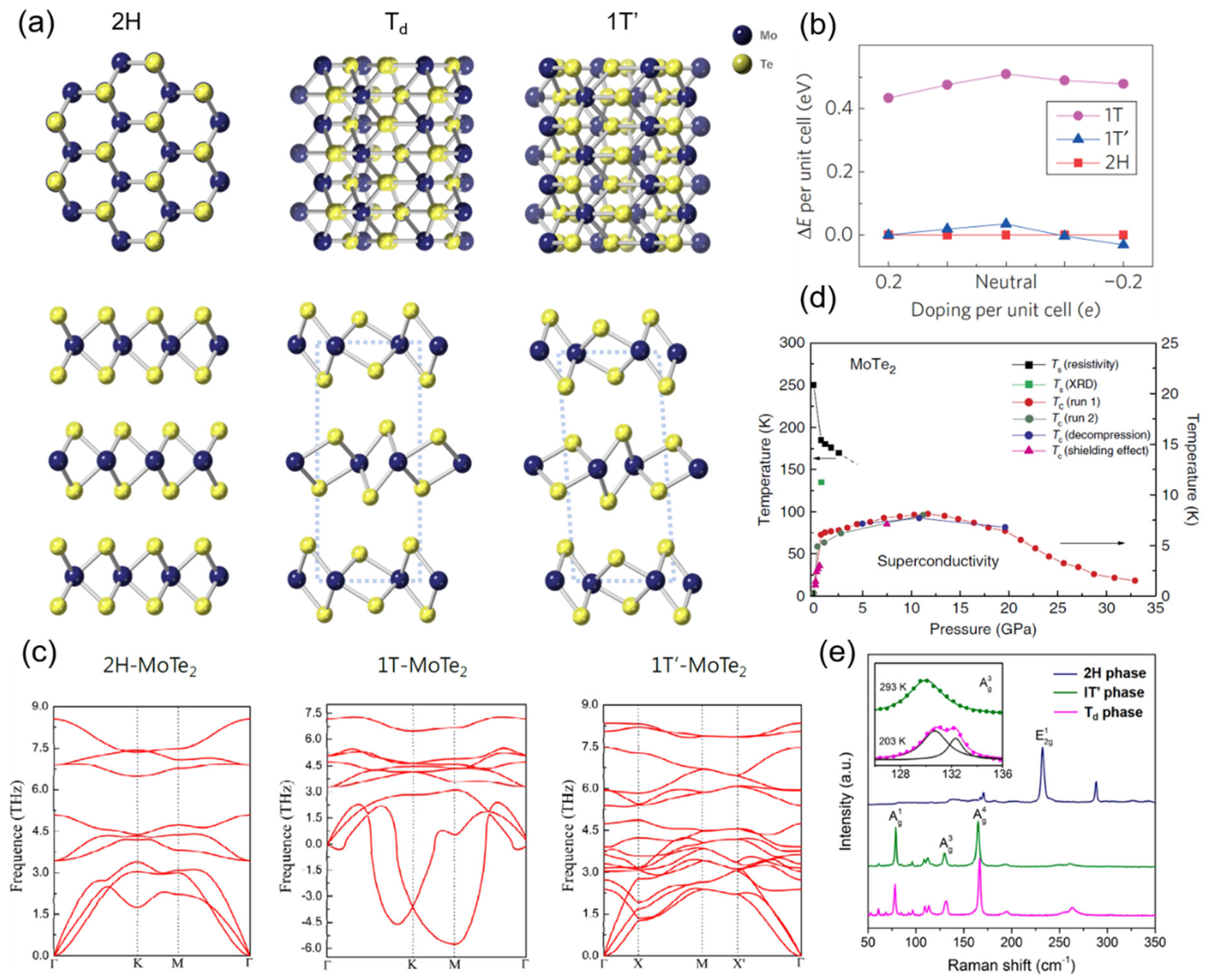
Near room temperature, MoTe2 exhibits three stable phases: 2H, 1T′, and Td phases. These phases have different lattice structures, band structures, and fingerprints in optical spectra.

2.1. 2H Phase

As shown in Figure 1a, 2H-MoTe2 (α-phase) exhibits a hexagonal structure, and it belongs to the space group P63/mmc with a honeycomb-like in-plane structure [28]. In addition, 2H-MoTe2 is an indirect bandgap semiconductor (bandgap 0.8 eV [29]) in bulk and few-layer states (Figure 1c). When thinned to a monolayer, however, it becomes a direct bandgap semiconductor (bandgap 1.1 eV [30]). Generally, 2H-MoTe2 is relatively stable in ambient conditions, but, due to the extremely small energy barrier with 1T′-MoTe2, it will convert into the 1T′ phase under excess Te deficiency or strain [31,32].

2.2. 1T′ Phase

Firstly, 1T′-MoTe2 (β-phase) has a monolithic structure, belonging to space group P21/m, with a distorted centered honeycomb in-plane structure and slightly inclined interplane structure (β angle = 93°55′) [28], as shown in Figure 1a. Compared to 2H-MoTe2, 1T′-MoTe2 is more vulnerable to oxidation [33]. In addition, 1T′-MoTe2 is generally acknowledged to be metallic, whether in the bulk or monolayer state. However, there are some reports designating few-layer 1T′-MoTe2 as a semiconductor. Keum et al. reported that few-layer 1T′-MoTe2 exhibited a bandgap opening up to 60 meV (Figure 1c) and proposed that it was induced by strong spin–orbit coupling (SOC) [17]. More recently, tri-layer 1T′-MoTe2 was reported to possess a narrow bandgap of 28 meV, but, in thicker MoTe2 samples (>4 nm), such bandgap opening was not observed [34]. On the contrary, it was also reported that tri-layer 1T′-MoTe2 remained free of a bandgap [35]. It is still under debate whether few-layer 1T′-MoTe2 has a bandgap.
In addition, 1T′-MoTe2 was reported to be a topological insulator as well as a room-temperature ferroelectric material. A weak antilocalization effect was observed in monolayer 1T′-MoTe2, indicating the presence of strong SOC, which is related to topological insulator materials [22]. Bulk 1T′-MoTe2 was predicted to be a Z4-nontrivial higher-order TI (HOTI) driven by double band inversion [23], which has not been experimentally confirmed yet. Recently, robust room-temperature out-of-plane ferroelectricity was observed in monolayer distorted 1T-MoTe2 [36], which has sparked the exploration of fundamental physics and promising applications at the monolayer limit.

2.3. Td Phase

Td-MoTe2 (γ-phase) has an orthogonal structure, belonging to space group Pmn21 [28]. Compared to the 1T′ phase, the Td phase displays a very similar but more regular structure (Figure 1a). From the cross-section direction, atoms in different layers of Td-MoTe2 are in good alignment with each other, whereas, in 1T′-MoTe2 atoms, layers slide a short distance and form a 0.94° tilt angle. Therefore, it is almost impossible to distinguish 1T′ from Td MoTe2 at the level of the monolayer.
When the temperature is increased above ~250 K, the Td phase is supposed to convert to the 1T′ phase [37]. In order to obtain stable Td-MoTe2 at room temperature, tungsten substitutional doping [38] and thinning the material to be below 10 nm [37,39] are effective strategies. Owing to its broken inversion symmetry, the Td phase possesses abundant physical properties, such as superconductivity and Type-II WSM.
Td-MoTe2 exhibits pressure- and thickness-dependent superconductivity. The transition temperature Tc of Td-MoTe2 increases with higher pressure and smaller thickness. The Tc of bulk Td-MoTe2 was reported to be 0.10 K (Figure 1d) [24]. Guguchia et al. observed the two-gap s-wave symmetry of the superconducting order parameter in Td-MoTe2, and suggested a higher possibility of a topologically non-trivial s+− state in Td-MoTe2 [40]. A fast-mode oscillation of the critical current Ic versus magnetic field B along the edge was observed in Td-MoTe2 by Wang et al., which was generated by fluxoid quantization and indicated the existence of a robust edge supercurrent [41]. As the breaking of the time-reversal symmetry or inversion symmetry is the prerequisite for WSM, Td-MoTe2 was predicted as a Type-II WSM due to its noncentrosymmetric lattice structure [26]. Kaminski et al. identified Fermi arcs, Weyl points, and novel surface states in bulk Td-MoTe2 with the angle-resolved photoemission spectroscopy (ARPES) technique, providing experimental evidence for Td-MoTe2 as a Type-II WSM [42]. Large magnetoresistance, a chiral-anomaly-related phenomenon, was reported in Td-MoTe2, further proving that Td-MoTe2 is a representative Type-II WSM [43,44].

3. Construction of 2D MoTe2 Hetero-Phase Homojunctions

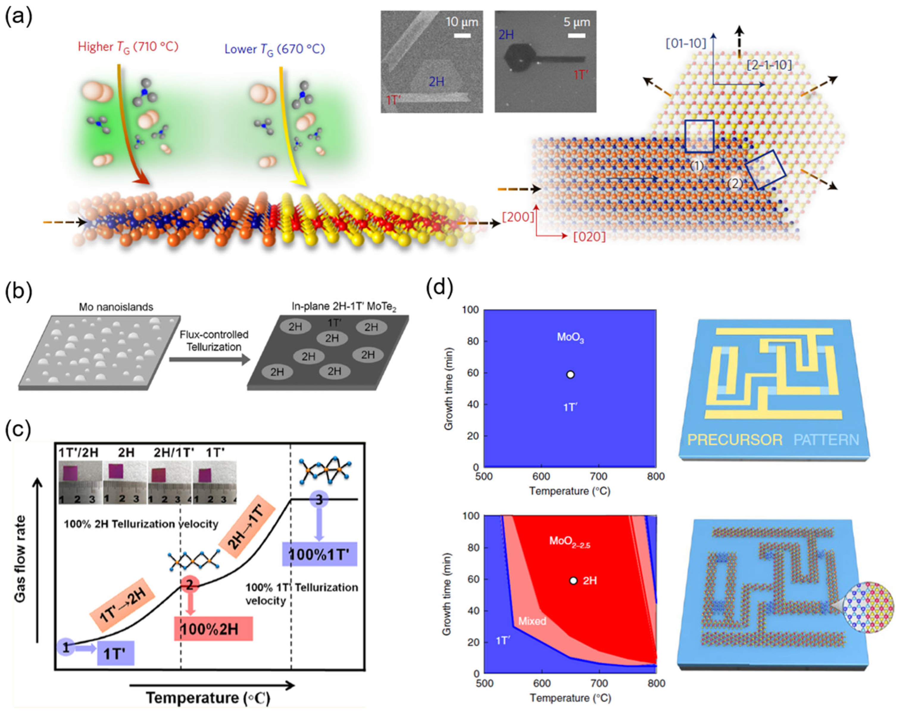
3.1. Direct Synthesis

Chemical vapor deposition (CVD) is a universal and convenient method for the direct synthesis of 2D materials and heterojunctions, which is also viable in the case of MoTe2 hetero-phase homojunctions. The key to constructing 2D MoTe2 hetero-phase homojunctions is precise control of phases. The final phase of MoTe2 after growth is determined by several factors, which are growth temperature, growth atmosphere, and Te vacancy concentration.
It was reported that the most thermodynamically stable phase varied under different processing temperatures [45]. Thus, by controlling the growth temperature, a certain phase can be selectively obtained. Sung et al. reported that the 1T′-phase was the dominant product at a higher temperature (710 °C), and the 2H phase dominated at a lower temperature (670 °C) [16]. By sequential growth of 1T′ and 2H-MoTe2, they obtained isolated lateral 1T′-2H-MoTe2 homojunctions (Figure 2a). With increasing temperature, Yang et al. observed the phase evolution shown in Figure 2c: pure 1T′-phase→1T′- and 2H-phase→pure 2H-phase→2H- and 1T′-phase→pure 1T′-phase [46].
Besides the growth temperature, the growth atmosphere plays an important role in controlling the phases in MoTe2. By changing the flow rate of either the inert carrier gas (N2) or active carrier gas (H2), phase evolutions with a tendency similar to the aforementioned were reported [46,47]. Such phase evolution was attributed to the tellurization velocity, and conclusions were drawn that a fast tellurization velocity favored 1T′ phase formation, while a moderate tellurization velocity favored the 2H phase [46]. It is possibly analogous to the formation of dendrites, wherein a fast cooling rate leads to plenty of dendrites, which possess a more disordered and defect-rich structure, while a moderate cooling rate results in a more regular and thermodynamically stable structure.
In essence, the process of phase transition in MoTe2 is structural transformation [48], which can be triggered by either external stimuli, such as temperature and growth rate, or internal factors such as strain and Te deficiency. The influence of strain in the phase control of MoTe2 will be discussed in the next section. The utility of the Te deficiency in the phase control of MoTe2 has been intensively studied. It was reported that the 1T′ phase of MoTe2 was more stable than the 2H phase when the Te deficiency exceeded 2%, which was confirmed by density functional theory (DFT) calculations [48]. In CVD synthesis, the concentration of Te deficiency is tunable by controlling the concentrations or compositions of precursors.
Strategies such as prolonging the growth time [49], increasing Te atomic flux by raising the source temperature (Figure 2b) [50], and controlling the concentration of MoO3 precursor by means of molecular sieves and overlapped substrates [51] were proven to be effective to provide excessive Te during the growth period and thereby obtain the stable stoichiometric 2H phase. Accordingly, the reverse phase transition from 2H to 1T′-MoTe2 could be realized by further annealing under a lower partial pressure of Te at the same temperature, followed by rapid quenching [49]. Moreover, a mixed-dimensional in-plane 1D–2D Mo6Te6–MoTe2 heterostructure was directly synthesized under medium Te flux [52].
By tellurizing precursors with different compositions, 2H and 1T′-MoTe2 were simultaneously synthesized by Zhang et al. [15]. The products after tellurizing MoO2.0–2.5 and MoO3 thin films were identified as 2H and 1T′-MoTe2, respectively (Figure 2d). The authors proposed that the selective phase synthesis was realized by the varied Te monovacancies densities in the products. Combining the above synthesis strategies with lithographic processes, 2D MoTe2 hetero-phase junctions [50,53] and their derivatives, such as MoTe2 field-effect transistor (FET) arrays [54,55] and integrated MoTe2 circuits [15], were successfully fabricated.
Recently, Xu et al. showed that the structure of 2H-MoTe2 could spread into the adjacent 1T′ phase under a Te-rich atmosphere [56]. Triggered by an implanted single-seed crystal, they synthesized wafer-scale single-crystalline 2H-MoTe2 via 2D epitaxy of polycrystalline 1T′-MoTe2.

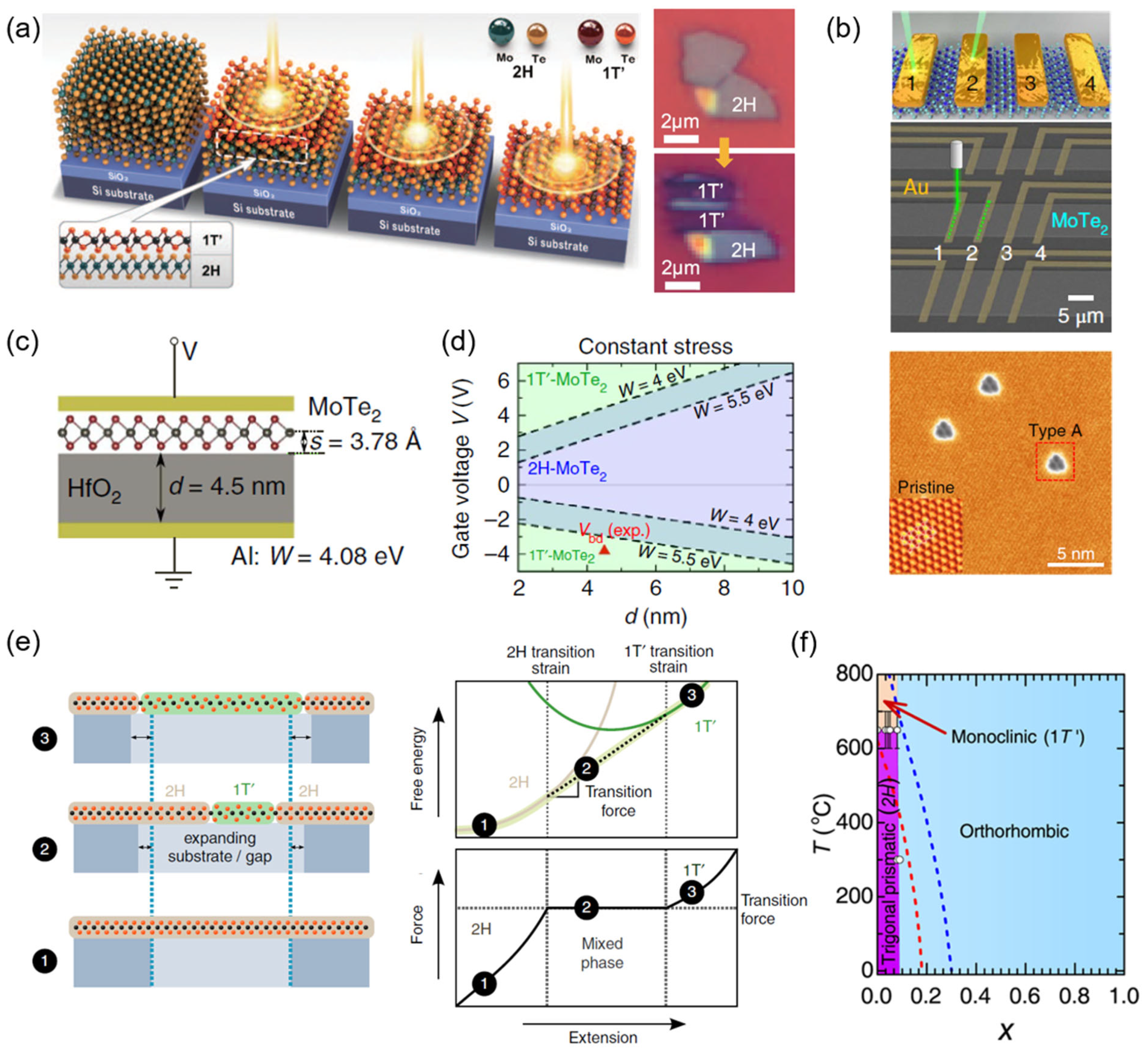
3.2. Post-Processing

Besides direct synthesis, post-processing is also a very versatile strategy to realize 2D MoTe2 hetero-phase homojunctions. Owing to the small energy barrier between the 2H and 1T′ phases, external stimuli, such as a laser, electrostatic gating, mechanical deformations, chalcogen alloying, and lithium-ion (Li+) intercalation, can easily induce phase transition in MoTe2.
Laser treatment was reported to induce Te vacancies in MoTe2, which thereafter triggered the local phase transition from the 2H phase to 1T′ phase [57,58,59]. Cho et al. used laser-induced phase patterning to fabricate an ohmic 2H–1T′ hetero-phase homojunction that was stable up to 300 °C (Figure 3a) [57]. Not only an ohmic contact between phases but also a patterned phase transfer area could be achieved by this method. By carefully adjusting the laser power and irradiation time, the structural phases of MoTe2 could be gradually controlled [60].
Similarly, a scanning visible light probe could be used to directly write electrical circuits onto 2H-MoTe2 thin films (Figure 3b) [61]. By creating adatom–vacancy clusters in the host lattice, laser light illumination on patterned metal deposited onto 2H-MoTe2 could locally convert the underneath area from an n-type semiconductor to a p-type semiconductor. This doping method could be utilized to assemble both n- and p-doped channels in the same atomic plane at the submicrometer scale, making it possible to fabricate 2D n–p–n (p–n–p) bipolar junction transistor amplifier arrays as well as radial p–n photovoltaic cells.
Electrostatic gating was expected to be a flexible and viable means of phase transition in MoTe2. Li et al. predicted the structural semiconductor-to-semimetal phase transition in monolayer MoTe2 induced by electrostatic gating [62]. In order to observe 2H–1T′ phase transition in undoped monolayer MoTe2 under the constant-stress circumstance, a surface charge density of <−0.04 e or >0.09 e per formula unit was found to be required. Employing a capacitor structure (Figure 3c), a gate voltage of 2–4 V was required to dynamically control the 2H–1T′ phase transition in monolayer MoTe2 (Figure 3d). In addition, alloying was predicted to effectively reduce the transition gate voltage—for example, down to 0.3–1 V for MoxW1−xTe2 monolayers.
As is mentioned above, lattice distortion can also lead to structural transition in MoTe2. Duerloo et al. predicted that mechanical deformations could induce phase transition between a semiconducting and a metallic crystal structure in Mo- and W-dichalcogenide monolayers (Figure 3e), and identified that, under uniaxial conditions at room temperature, MoTe2 required tensile strains ranging from 0.3 to 3% to have phase transition [63]. Subsequently, a room-temperature 2H–1T′ transition in a MoTe2 thin film induced experimentally by a tensile strain of 0.2% was reported [64]. A 2H-MoTe2 thin film was transferred to a patterned Si/SiO2 substrate with cavities of different diameters, and the researchers then introduced tensile strain using an atomic force microscope (AFM) tip. The supported area without strain remained semiconducting, the suspended area exhibited metallic properties, and the peripheral area displayed both 1T′ and 2H Raman signals. After the release of the strain, the semiconductor–metal phase transition at room temperature was found to be reversible under ambient conditions, which was attributed to the large volume change and small latent heat during the phase transition.
Chalcogen alloying was first introduced to assist electrostatic gating by significantly reducing the transition gate voltage, but, later, alloying alone was found to effectively control the phases of MoTe2. Duerloo et al. predicted the structural phase transitions of alloyed MoTe2-WTe2 monolayers with phase transition temperatures ranging from 0 to 933 K, and mapped its temperature–composition phase diagrams by DFT calculations [65]. Zhang et al. investigated the effect of electrostatic charge injection on the phase stability of monolayer MoTe2 and WTe2, as well as the effect of transition metal alloying on the phase stability of the H and the T′ phases in monolayer WxMo1−xTe2 using DFT calculations [66]. Rhodes et al. successfully engineered the phases of MoTe2 through W substitution, and plotted the phase diagram of the Mo1−xWxTe2 solid solution (Figure 3f), which exhibited a semiconducting to semi-metallic transition as a function of x [38]. A small critical W concentration xc ~ 8% was reported to stabilize the γ-phase, which possessed a Fermi surface near that of WTe2 at room temperature. The effect of chalcogen alloying on the energy difference and stability between the H and T′ phases in monolayer MoTe2 was then studied by DFT calculations [67]. Seven MoTe2−xXx alloys (X = N, P, Sb, F, Br, I, and Se) at three concentrations were investigated, and the energy difference between the H and T′ phases was found to be reliant on the chemistry, size, and concentration of the dopants. The p-type and n-type dopants were reported to contribute to defect states atop the valence band and states at the Fermi level of MoTe2, respectively.
Li+ intercalation was predicted to be possible by DFT calculations to induce phase transition in MoTe2 by intercalating Li+ ions energetically stable on the 1T′ phase [68]. Utilizing a convection-assisted Li+ intercalation method, Eshete et al. converted the surfaces of single-crystalline 2H-MoTe2 into the 1T′ phase, and fabricated a vertical 1T′–2H–1T′ MoTe2 homojunction [69]. Such a vertical hetero-phase junction was expected to allow active charge transfer and provide numerous catalytic active sites, exhibiting great potential in electrochemical catalysis applications.

4. Applications of 2D MoTe2 Hetero-Phase Homojunctions

4.1. Electronic Devices

Transistors with ohmic contacts have always been in great demand in the semiconductor industry due to their high performance and low power consumption [70,71]. However, the external metal electrodes in transistors tend to induce not only high SBH, resulting from Fermi-level pinning, but also impurities and defects owing to the multi-step procedures of device fabrication, which leads to severe deterioration in device performance [72]. Two-dimensional MoTe2 hetero-phase homojunctions provide a solution to these problems. Owing to the small energy barrier between the metallic 1T′ phase and semiconducting 2H phase, the coexistence of the two phases is attainable in transistors as electrodes and channels, respectively. If covalently bonded and atomically coherent, the hetero-phase interface in MoTe2 is anticipated to possess an ultralow SBH [16], which incidentally avoids contamination introduced by external metal contacts and unnecessary film depositions. Thus, there are high hopes for 2D MoTe2 hetero-phase homojunctions in applications involving electronic devices.

4.1.1. Transistors

Transistors are the basic components of IC, where 2D MoTe2 hetero-phase homojunctions have found their way towards high performance. Sung et al. found that the coplanar contacted 1T′–2H MoTe2 FETs outperformed conventional Au top-contacted FETs, with significantly higher gate tunability and on current (Figure 4a,b) [16]. By analyzing energy band diagram models and experimental results of the temperature-dependent conductance of FETs at various gate voltages Vg, they found an ultralow SBH (~25 meV) of the atomically coherent 1T′–2H MoTe2 coplanar contact. Similar experimental results in lateral polymorphic MoTe2 homojunction FETs fabricated by flux-controlled phase engineering were reported [15,54,73].
The mechanism of the reduced contact resistance in monolayer coplanar polymorphic MX2 (MoS2, WS2, MoSe2, WSe2, MoTe2) FETs with the 2H phase as channels and 1T′ phase as electrodes was demonstrated via ab initio quantum transport simulations [75]. MIGS at the interface was revealed to penetrate the Schottky barrier and connect the valence/conduction band of the channel and the electrodes, consequently leading to a tunable and lower effective SBH and an equivalent ohmic contact under a proper gate voltage. The electronic and contact properties of twelve interface structures of monolayer coplanar 2H–1T′-MoTe2 interfaces were investigated using first-principles calculations [76]. The two most energy-favored structures were named as (0°, 30°) and (0°, −30°), and the former was predicted to possess a small SBH, while the Fermi level of the latter was anticipated to be located near the midgap.
Taking advantage of the ultralow contact resistance in 2D MoTe2 hetero-phase homojunctions, various applications based on polymorphic MoTe2 transistors were exploited—for example, MoTe2 radiofrequency (RF) transistors with excellent air stability and a remarkable cutoff frequency (320 MHz with a 5 μm gate length), an ultrashort-gate-length 1T′–2H-MoTe2 FET based on a CNT gate with a small subthreshold swing (~73 mV dec−1) and a high on/off current ratio (~105), and three-dimensional IC by assembling layers of phase-patterned MoTe2 [15].

4.1.2. Logical Devices

By tellurizing patterned different precursors, arrays of hetero-phase MoTe2 logic inverters were prepared, which exhibited excellent logic-level conservation, good air stability, and eligibility for IC composed of multiple cascaded inverters (Figure 4c,d) [15]. Under the electric-field-induced strain generated by a ferroelectric substrate, Hou et al. observed the reversible phase transition between few-layer 1T′ and 2H-MoTe2 in an FET geometry [73]. This new strategy for transistor switching circumvented the problems of static and dynamic power consumption in conventional FETs. They achieved large nonvolatile changes in channel conductivity between two states at room temperature (Figure 4g–i), indicating the great potential of the sub-nanosecond low-power non-volatile strain switching strategy for applications such as logic and memory devices.

4.1.3. Memory Devices

In vertical 2H-MoTe2/Mo1−xWxTe2 resistive random access memory (RRAM) devices, Zhang et al. reported an electric-field-induced phase transition from 2H to 2Hd (a distorted transient structure) and the Td phase [29]. They achieved ultrafast, reproducible, resistive switching with on/off current ratios of 106 and programming currents lower than 1 μA in a selectorless RRAM architecture utilizing an Al2O3/MoTe2 stack (Figure 4e,f).

4.1.4. Capacitors

Mixed-dimensional MoTe2 structures have shown impressive potential in energy conversion applications. A supercapacitor based on an integrated structure of few-layer 2H-MoTe2 and 1T′-Mo6Te6 nanoplates (NPs) was reported to exhibit enhanced areal capacitance (1542 mF cm−2 at 10 mV s−1) compared with a transferred monolayer mixed-dimensional electrode, as well as a high energy density (140.36 mW cm−2 at 4 mA) and excellent electrochemical stability (96%) [77]. This was attributed to the synergistic effect of 1D Mo6Te6 NPs and 2D MoTe2 layers in the integrated structure, which provided a large surface area and highly conductive pathway, enabling K+ ions to diffuse effectively and favoring rapid reversible redox reactions.

4.2. Optoelectronic Devices

As is mentioned above, few-layer 2H-MoTe2 possesses an indirect bandgap of 0.8 eV, which is suitable for near-infrared (NIR) photodetection [78]. The photogating effect was considered to dominate the photocurrent generation in few-layer 2H-MoTe2-based photodetectors and the detailed mechanism was demonstrated as follows: after the generation of electron–hole pairs under irradiation, the charged trap states in the channel acted as a local floating gate and induced more electrons by trapping holes, leading to effective tuning of the channel conductance [79,80].
For MoTe2 hetero-phase homojunctions, photodetectors with both lateral and vertical structures were reported. Via a two-step patterned CVD growth and transfer method, Xu et al. fabricated a lateral 1T′–2H–1T′-MoTe2 hetero-phase FET array on a flexible polyimide substrate [54]. They measured the NIR photoresponsivity of the hetero-phase photodetector under different incident light powers and showed a high NIR photoresponsivity of ~1.02 A/W (Figure 5a–c). Lin et al. constructed a vertical 1T′–2H-MoTe2 hetero-phase photodetectors and compared the optical response properties to that without inserting 1T′-MoTe2 interlayer contact [81].

4.3. Electrocatalysis Materials

Furthermore, 1T′-MoTe2 was reported to have significant potential in electrocatalysis. Resulting from the adsorption of H atoms onto Te sites on the surface, 1T′-MoTe2 exhibited a rapid and reversible activation process where the overpotential required to maintain a certain current density decreased significantly when held at cathodic bias [83].
Chen et al. illustrated that 2H–1T′ phase boundaries could effectively activate the basal plane of monolayer MoTe2 for enhanced hydrogen evolution reaction (HER) performance [82]. They investigated, by first-principles calculations, the structural and energetics stabilities of possible configurations of the 2H–1T′ phase boundary, including Te, Mo, and hollow sites, which were identified as possible catalytic centers for the HER at energetically stable phase boundaries (Figure 5d). In particular, the hollow sites newly induced by phase boundaries exhibited comparable Gibbs free energy to that of Pt near the thermoneutral value for H2 adsorption (Figure 5e), which was due to the unique electronic structures and local geometries of H2 adsorption at phase boundaries.

5. Summary and Prospects

In this short review, we summarized the recent progress in 2D MoTe2 hetero-phase homojunctions. We first briefly introduced the properties of three phases of MoTe2, namely the 2H, 1T′, and Td phases, and then illustrated two strategies, direct synthesis and post-processing, to construct 2D MoTe2 hetero-phase homojunctions. We also enumerated the applications of 2D MoTe2 hetero-phase homojunctions in electronics, optoelectronics, and electrocatalysis.
Despite the fascinating prospects, 2D MoTe2 hetero-phase homojunctions are confronted with several challenges. First, the synthesis and characterization of monolayer MoTe2 hetero-phase homojunctions remain to be accomplished, which requires precise control of thickness and careful protection from degradation. Second, to be compatible with the semiconductor industry, facile methods of constructing large-scale patterned MoTe2 hetero-phase homojunction arrays are in demand. Lastly, MoTe2 hetero-phase homojunctions involving the Td phase and other transient phases beyond need to be further explored.
Various challenges notwithstanding, 2D MoTe2 hetero-phase homojunctions are expected to be a stepping stone to super-large-scale IC with extremely high integrity based on pure 2D materials, a fabulous platform for emerging physics research, as well as a promising candidate for future applications.

Author Contributions

Writing—original draft preparation, J.G.; writing—review and editing, J.G. and K.L.; supervision, K.L.; funding acquisition, K.L. All authors have read and agreed to the published version of the manuscript.

Funding

This work was financially supported by the Basic Science Center Project of NSFC under grant no. 51788104, the National Key R&D Program of China (2018YFA0208400), and the National Natural Science Foundation of China under grant nos. 51972193 and 11774191.

Institutional Review Board Statement

Not applicable.

Informed Consent Statement

Not applicable.

Data Availability Statement

Not applicable.

Conflicts of Interest

The authors declare no conflict of interest.

References

  1. Moore, G.E. Cramming more components onto integrated circuits, Reprinted from Electronics, volume 38, number 8, April 19, 1965, pp.114 ff. IEEE Solid-State Circuits Soc. Newsl. 2006, 11, 33–35. [Google Scholar] [CrossRef]
  2. Packan, P.A. Pushing the Limits. Science 1999, 285, 2079–2081. [Google Scholar] [CrossRef]
  3. Lundstrom, M. Applied physics. Moore’s law forever? Science 2003, 299, 210–211. [Google Scholar] [CrossRef] [PubMed]
  4. Young, K.K. Short-channel effect in fully depleted SOI MOSFETs. IEEE Trans. Electron. Devices 1989, 36, 399–402. [Google Scholar] [CrossRef]
  5. Bin, Y.; Wann, C.H.J.; Nowak, E.D.; Noda, K.; Chenming, H. Short-channel effect improved by lateral channel-engineering in deep-submicronmeter MOSFET′s. IEEE Trans. Electron. Devices 1997, 44, 627–634. [Google Scholar] [CrossRef]
  6. Bar-Yam, Y.; Joannopoulos, J.D. Dangling bond in a-Si:H. Phys. Rev. Lett. 1986, 56, 2203–2206. [Google Scholar] [CrossRef] [PubMed]
  7. Zhang, S.B.; Wei, S.H. Surface energy and the common dangling bond rule for semiconductors. Phys. Rev. Lett 2004, 92, 086102. [Google Scholar] [CrossRef] [PubMed]
  8. Liu, Y.; Duan, X.; Shin, H.J.; Park, S.; Huang, Y.; Duan, X. Promises and prospects of two-dimensional transistors. Nature 2021, 591, 43–53. [Google Scholar] [CrossRef]
  9. Tung, R.T. The physics and chemistry of the Schottky barrier height. Appl. Phys. Rev. 2014, 1, 011304. [Google Scholar]
  10. Shen, P.C.; Su, C.; Lin, Y.; Chou, A.S.; Cheng, C.C.; Park, J.H.; Chiu, M.H.; Lu, A.Y.; Tang, H.L.; Tavakoli, M.M.; et al. Ultralow contact resistance between semimetal and monolayer semiconductors. Nature 2021, 593, 211–217. [Google Scholar] [CrossRef]
  11. Louie, S.G.; Cohen, M.L. Electronic structure of a metal-semiconductor interface. Phys. Rev. B 1976, 13, 2461–2469. [Google Scholar] [CrossRef]
  12. Nishimura, T.; Kita, K.; Toriumi, A. Evidence for strong Fermi-level pinning due to metal-induced gap states at metal/germanium interface. Appl. Phys. Lett. 2007, 91, 123123. [Google Scholar] [CrossRef]
  13. Sotthewes, K.; van Bremen, R.; Dollekamp, E.; Boulogne, T.; Nowakowski, K.; Kas, D.; Zandvliet, H.J.W.; Bampoulis, P. Universal Fermi-Level Pinning in Transition-Metal Dichalcogenides. J. Phys. Chem. C Nanomater. Interfaces 2019, 123, 5411–5420. [Google Scholar] [CrossRef] [Green Version]
  14. Manzeli, S.; Ovchinnikov, D.; Pasquier, D.; Yazyev, O.V.; Kis, A. 2D transition metal dichalcogenides. Nat. Rev. Mater. 2017, 2, 17033. [Google Scholar] [CrossRef]
  15. Zhang, Q.; Wang, X.-F.; Shen, S.-H.; Lu, Q.; Liu, X.; Li, H.; Zheng, J.; Yu, C.-P.; Zhong, X.; Gu, L.; et al. Simultaneous synthesis and integration of two-dimensional electronic components. Nat. Electron. 2019, 2, 164–170. [Google Scholar] [CrossRef]
  16. Sung, J.H.; Heo, H.; Si, S.; Kim, Y.H.; Noh, H.R.; Song, K.; Kim, J.; Lee, C.S.; Seo, S.Y.; Kim, D.H.; et al. Coplanar semiconductor-metal circuitry defined on few-layer MoTe2 via polymorphic heteroepitaxy. Nat. Nanotechnol. 2017, 12, 1064–1070. [Google Scholar] [CrossRef] [PubMed]
  17. Keum, D.H.; Cho, S.; Kim, J.H.; Choe, D.-H.; Sung, H.-J.; Kan, M.; Kang, H.; Hwang, J.-Y.; Kim, S.W.; Yang, H.; et al. Bandgap opening in few-layered monoclinic MoTe2. Nat. Phys. 2015, 11, 482–486. [Google Scholar] [CrossRef]
  18. Sun, Y.; Pan, J.; Zhang, Z.; Zhang, K.; Liang, J.; Wang, W.; Yuan, Z.; Hao, Y.; Wang, B.; Wang, J.; et al. Elastic Properties and Fracture Behaviors of Biaxially Deformed, Polymorphic MoTe2. Nano Lett. 2019, 19, 761–769. [Google Scholar] [CrossRef] [PubMed]
  19. Mortazavi, B.; Berdiyorov, G.R.; Makaremi, M.; Rabczuk, T. Mechanical responses of two-dimensional MoTe2; pristine 2H, 1T and 1T′ and 1T′/2H heterostructure. Extreme Mech. Lett. 2018, 20, 65–72. [Google Scholar] [CrossRef] [Green Version]
  20. Zhang, Y.-J.; Wang, R.-N.; Dong, G.-Y.; Wang, S.-F.; Fu, G.-S.; Wang, J.-L. Mechanical properties of 1T-, 1T′-, and 1H-MX2 monolayers and their 1H/1T′-MX2 (M = Mo, W and X = S, Se, Te) heterostructures. AIP Adv. 2019, 9, 125208. [Google Scholar] [CrossRef] [Green Version]
  21. Fu, L.; Kane, C.L.; Mele, E.J. Topological insulators in three dimensions. Phys. Rev. Lett. 2007, 98, 106803. [Google Scholar] [CrossRef] [Green Version]
  22. Naylor, C.H.; Parkin, W.M.; Ping, J.; Gao, Z.; Zhou, Y.R.; Kim, Y.; Streller, F.; Carpick, R.W.; Rappe, A.M.; Drndic, M.; et al. Monolayer Single-Crystal 1T′-MoTe2 Grown by Chemical Vapor Deposition Exhibits Weak Antilocalization Effect. Nano Lett. 2016, 16, 4297–4304. [Google Scholar] [CrossRef] [PubMed] [Green Version]
  23. Wang, Z.; Wieder, B.J.; Li, J.; Yan, B.; Bernevig, B.A. Higher-Order Topology, Monopole Nodal Lines, and the Origin of Large Fermi Arcs in Transition Metal Dichalcogenides XTe2 (X = Mo, W). Phys. Rev. Lett. 2019, 123, 186401. [Google Scholar] [CrossRef] [PubMed] [Green Version]
  24. Qi, Y.; Naumov, P.G.; Ali, M.N.; Rajamathi, C.R.; Schnelle, W.; Barkalov, O.; Hanfland, M.; Wu, S.C.; Shekhar, C.; Sun, Y.; et al. Superconductivity in Weyl semimetal candidate MoTe2. Nat. Commun. 2016, 7, 11038. [Google Scholar] [CrossRef] [PubMed] [Green Version]
  25. Soluyanov, A.A.; Gresch, D.; Wang, Z.; Wu, Q.; Troyer, M.; Dai, X.; Bernevig, B.A. Type-II Weyl semimetals. Nature 2015, 527, 495–498. [Google Scholar] [CrossRef] [Green Version]
  26. Sun, Y.; Wu, S.-C.; Ali, M.N.; Felser, C.; Yan, B. Prediction of Weyl semimetal in orthorhombic MoTe2. Phys. Rev. B 2015, 92, 161107. [Google Scholar] [CrossRef] [Green Version]
  27. Wang, Z.; Gresch, D.; Soluyanov, A.A.; Xie, W.; Kushwaha, S.; Dai, X.; Troyer, M.; Cava, R.J.; Bernevig, B.A. MoTe2: A Type-II Weyl Topological Metal. Phys. Rev. Lett. 2016, 117, 056805. [Google Scholar] [CrossRef] [Green Version]
  28. Dawson, W.G.; Bullett, D.W. Electronic structure and crystallography of MoTe2 and WTe2. J. Phys. C Solid State Phys. 1987, 20, 6159–6174. [Google Scholar] [CrossRef]
  29. Zhang, F.; Zhang, H.; Krylyuk, S.; Milligan, C.A.; Zhu, Y.; Zemlyanov, D.Y.; Bendersky, L.A.; Burton, B.P.; Davydov, A.V.; Appenzeller, J. Electric-field induced structural transition in vertical MoTe2- and Mo1−xWxTe2-based resistive memories. Nat. Mater. 2019, 18, 55–61. [Google Scholar] [CrossRef]
  30. Ruppert, C.; Aslan, O.B.; Heinz, T.F. Optical properties and band gap of single- and few-layer MoTe2 crystals. Nano Lett. 2014, 14, 6231–6236. [Google Scholar] [CrossRef]
  31. Tang, Q. Tuning the phase stability of Mo-based TMD monolayers through coupled vacancy defects and lattice strain. J. Mater. Chem. C 2018, 6, 9561–9568. [Google Scholar] [CrossRef]
  32. Zhu, H.; Wang, Q.; Cheng, L.; Addou, R.; Kim, J.; Kim, M.J.; Wallace, R.M. Defects and Surface Structural Stability of MoTe2 Under Vacuum Annealing. ACS Nano 2017, 11, 11005–11014. [Google Scholar] [CrossRef]
  33. Yang, L.; Wu, H.; Zhang, W.; Chen, Z.; Li, J.; Lou, X.; Xie, Z.; Zhu, R.; Chang, H. Anomalous oxidation and its effect on electrical transport originating from surface chemical instability in large-area, few-layer 1T′-MoTe2 films. Nanoscale 2018, 10, 19906–19915. [Google Scholar] [CrossRef]
  34. Park, J.C.; Jung, E.; Lee, S.; Hwang, J.; Lee, Y.H. Evidence of shallow band gap in ultrathin 1T′-MoTe2 via infrared spectroscopy. Phys. Rev. B 2020, 101, 235434. [Google Scholar] [CrossRef]
  35. Song, P.; Hsu, C.; Zhao, M.; Zhao, X.; Chang, T.-R.; Teng, J.; Lin, H.; Loh, K.P. Few-layer 1T′ MoTe2 as gapless semimetal with thickness dependent carrier transport. 2D Mater. 2018, 5, 031010. [Google Scholar] [CrossRef]
  36. Yuan, S.; Luo, X.; Chan, H.L.; Xiao, C.; Dai, Y.; Xie, M.; Hao, J. Room-temperature ferroelectricity in MoTe2 down to the atomic monolayer limit. Nat. Commun. 2019, 10, 1775. [Google Scholar] [CrossRef] [PubMed] [Green Version]
  37. Cui, J.; Li, P.; Zhou, J.; He, W.Y.; Huang, X.; Yi, J.; Fan, J.; Ji, Z.; Jing, X.; Qu, F.; et al. Transport evidence of asymmetric spin-orbit coupling in few-layer superconducting 1Td-MoTe2. Nat. Commun. 2019, 10, 2044. [Google Scholar] [CrossRef]
  38. Rhodes, D.; Chenet, D.A.; Janicek, B.E.; Nyby, C.; Lin, Y.; Jin, W.; Edelberg, D.; Mannebach, E.; Finney, N.; Antony, A.; et al. Engineering the Structural and Electronic Phases of MoTe2 through W Substitution. Nano Lett. 2017, 17, 1616–1622. [Google Scholar] [CrossRef] [Green Version]
  39. He, R.; Zhong, S.; Kim, H.H.; Ye, G.; Ye, Z.; Winford, L.; McHaffie, D.; Rilak, I.; Chen, F.; Luo, X.; et al. Dimensionality-driven orthorhombic MoTe2 at room temperature. Phys. Rev. B 2018, 97, 041410. [Google Scholar] [CrossRef] [Green Version]
  40. Guguchia, Z.; von Rohr, F.; Shermadini, Z.; Lee, A.T.; Banerjee, S.; Wieteska, A.R.; Marianetti, C.A.; Frandsen, B.A.; Luetkens, H.; Gong, Z.; et al. Signatures of the topological s+- superconducting order parameter in the type-II Weyl semimetal Td-MoTe2. Nat. Commun. 2017, 8, 1082. [Google Scholar] [CrossRef] [Green Version]
  41. Wang, W.; Kim, S.; Liu, M.; Cevallos, F.A.; Cava, R.J.; Ong, N.P. Evidence for an edge supercurrent in the Weyl superconductor MoTe2. Science 2020, 368, 534–537. [Google Scholar] [CrossRef] [PubMed]
  42. Huang, L.; McCormick, T.M.; Ochi, M.; Zhao, Z.; Suzuki, M.T.; Arita, R.; Wu, Y.; Mou, D.; Cao, H.; Yan, J.; et al. Spectroscopic evidence for a type II Weyl semimetallic state in MoTe2. Nat. Mater. 2016, 15, 1155–1160. [Google Scholar] [CrossRef] [Green Version]
  43. Chen, F.C.; Lv, H.Y.; Luo, X.; Lu, W.J.; Pei, Q.L.; Lin, G.T.; Han, Y.Y.; Zhu, X.B.; Song, W.H.; Sun, Y.P. Extremely large magnetoresistance in the type-II Weyl semimetal MoTe2. Phys. Rev. B 2016, 94, 235154. [Google Scholar] [CrossRef] [Green Version]
  44. Lee, S.; Jang, J.; Kim, S.-I.; Jung, S.-G.; Kim, J.; Cho, S.; Kim, S.W.; Rhee, J.Y.; Park, K.-S.; Park, T. Origin of extremely large magnetoresistance in the candidate type-II Weyl semimetal MoTe2-x. Sci. Rep. 2018, 8, 13937. [Google Scholar] [CrossRef] [PubMed]
  45. Empante, T.A.; Zhou, Y.; Klee, V.; Nguyen, A.E.; Lu, I.H.; Valentin, M.D.; Naghibi Alvillar, S.A.; Preciado, E.; Berges, A.J.; Merida, C.S.; et al. Chemical Vapor Deposition Growth of Few-Layer MoTe2 in the 2H, 1T′, and 1T Phases: Tunable Properties of MoTe2 Films. ACS Nano 2017, 11, 900–905. [Google Scholar] [CrossRef]
  46. Yang, L.; Zhang, W.; Li, J.; Cheng, S.; Xie, Z.; Chang, H. Tellurization Velocity-Dependent Metallic-Semiconducting-Metallic Phase Evolution in Chemical Vapor Deposition Growth of Large-Area, Few-Layer MoTe2. ACS Nano 2017, 11, 1964–1972. [Google Scholar] [CrossRef]
  47. Kim, T.; Park, H.; Joung, D.; Kim, D.; Lee, R.; Shin, C.H.; Diware, M.; Chegal, W.; Jeong, S.H.; Shin, J.C.; et al. Wafer-Scale Epitaxial 1T′, 1T′-2H Mixed, and 2H Phases MoTe2 Thin Films Grown by Metal-Organic Chemical Vapor Deposition. Adv. Mater. Interfaces 2018, 5, 1800439. [Google Scholar] [CrossRef]
  48. Xu, X.; Chen, S.; Liu, S.; Cheng, X.; Xu, W.; Li, P.; Wan, Y.; Yang, S.; Gong, W.; Yuan, K.; et al. Millimeter-Scale Single-Crystalline Semiconducting MoTe2 via Solid-to-Solid Phase Transformation. J. Am. Chem Soc. 2019, 141, 2128–2134. [Google Scholar] [CrossRef]
  49. Park, J.C.; Yun, S.J.; Kim, H.; Park, J.H.; Chae, S.H.; An, S.J.; Kim, J.G.; Kim, S.M.; Kim, K.K.; Lee, Y.H. Phase-Engineered Synthesis of Centimeter-Scale 1T′- and 2H-Molybdenum Ditelluride Thin Films. ACS Nano 2015, 9, 6548–6554. [Google Scholar] [CrossRef]
  50. Yoo, Y.; DeGregorio, Z.P.; Su, Y.; Koester, S.J.; Johns, J.E. In-Plane 2H-1T′ MoTe2 Homojunctions Synthesized by Flux-Controlled Phase Engineering. Adv. Mater. 2017, 29, 1605461. [Google Scholar] [CrossRef]
  51. Zhou, L.; Xu, K.; Zubair, A.; Zhang, X.; Ouyang, F.; Palacios, T.; Dresselhaus, M.S.; Li, Y.; Kong, J. Role of Molecular Sieves in the CVD Synthesis of Large-Area 2D MoTe2. Adv. Funct. Mater. 2017, 27, 1603491. [Google Scholar] [CrossRef]
  52. Kim, H.; Johns, J.E.; Yoo, Y. Mixed-Dimensional In-Plane Heterostructures from 1D Mo6Te6 and 2D MoTe2 Synthesized by Te-Flux-Controlled Chemical Vapor Deposition. Small 2020, 16, 2002849. [Google Scholar] [CrossRef]
  53. Xie, Z.; Lei, W.; Zhang, W.; Liu, Y.; Yang, L.; Wen, X.; Chang, H. High-Performance Large-Scale Vertical 1T′/2H Homojunction CVD-Grown Polycrystalline MoTe2 Transistors. Adv. Mater. Interfaces 2021, 8, 2002023. [Google Scholar] [CrossRef]
  54. Xu, X.; Liu, S.; Han, B.; Han, Y.; Yuan, K.; Xu, W.; Yao, X.; Li, P.; Yang, S.; Gong, W.; et al. Scaling-up Atomically Thin Coplanar Semiconductor-Metal Circuitry via Phase Engineered Chemical Assembly. Nano Lett. 2019, 19, 6845–6852. [Google Scholar] [CrossRef] [PubMed] [Green Version]
  55. Yang, S.; Xu, X.; Xu, W.; Han, B.; Ding, Z.; Gu, P.; Gao, P.; Ye, Y. Large-Scale Vertical 1T′/2H MoTe2 Nanosheet-Based Heterostructures for Low Contact Resistance Transistors. ACS Appl. Nano Mater. 2020, 3, 10411–10417. [Google Scholar] [CrossRef]
  56. Xu, X.; Pan, Y.; Liu, S.; Han, B.; Gu, P.; Li, S.; Xu, W.; Peng, Y.; Han, Z.; Chen, J.; et al. Seeded 2D epitaxy of large-area single-crystal films of the van der Waals semiconductor 2H MoTe2. Science 2021, 372, 195–200. [Google Scholar] [CrossRef] [PubMed]
  57. Cho, S.; Kim, S.; Kim, J.H.; Zhao, J.; Seok, J.; Keum, D.H.; Baik, J.; Choe, D.-H.; Chang, K.J.; Suenaga, K.; et al. Phase patterning for ohmic homojunction contact in MoTe2. Science 2015, 349, 625–628. [Google Scholar] [CrossRef]
  58. Peng, B.; Zhang, H.; Chen, W.; Hou, B.; Qiu, Z.-J.; Shao, H.; Zhu, H.; Monserrat, B.; Fu, D.; Weng, H.; et al. Sub-picosecond photo-induced displacive phase transition in two-dimensional MoTe2. Npj 2D Mater. Appl. 2020, 4, 14. [Google Scholar] [CrossRef]
  59. Si, C.; Choe, D.; Xie, W.; Wang, H.; Sun, Z.; Bang, J.; Zhang, S. Photoinduced Vacancy Ordering and Phase Transition in MoTe2. Nano Lett. 2019, 19, 3612–3617. [Google Scholar] [CrossRef]
  60. Tan, Y.; Luo, F.; Zhu, M.; Xu, X.; Ye, Y.; Li, B.; Wang, G.; Luo, W.; Zheng, X.; Wu, N.; et al. Controllable 2H-to-1T′ phase transition in few-layer MoTe2. Nanoscale 2018, 10, 19964–19971. [Google Scholar] [CrossRef] [PubMed]
  61. Seo, S.-Y.; Park, J.; Park, J.; Song, K.; Cha, S.; Sim, S.; Choi, S.-Y.; Yeom, H.W.; Choi, H.; Jo, M.-H. Writing monolithic integrated circuits on a two-dimensional semiconductor with a scanning light probe. Nat. Electron. 2018, 1, 512–517. [Google Scholar] [CrossRef]
  62. Li, Y.; Duerloo, K.-A.N.; Wauson, K.; Reed, E.J. Structural semiconductor-to-semimetal phase transition in two-dimensional materials induced by electrostatic gating. Nat. Commun. 2016, 7, 10671. [Google Scholar] [CrossRef] [PubMed]
  63. Duerloo, K.A.; Li, Y.; Reed, E.J. Structural phase transitions in two-dimensional Mo- and W-dichalcogenide monolayers. Nat. Commun 2014, 5, 4214. [Google Scholar] [CrossRef] [Green Version]
  64. Song, S.; Keum, D.H.; Cho, S.; Perello, D.; Kim, Y.; Lee, Y.H. Room Temperature Semiconductor-Metal Transition of MoTe2 Thin Films Engineered by Strain. Nano Lett. 2016, 16, 188–193. [Google Scholar] [CrossRef]
  65. Duerloo, K.A.; Reed, E.J. Structural Phase Transitions by Design in Monolayer Alloys. ACS Nano 2016, 10, 289–297. [Google Scholar] [CrossRef]
  66. Zhang, C.; Kc, S.; Nie, Y.; Liang, C.; Vandenberghe, W.G.; Longo, R.C.; Zheng, Y.; Kong, F.; Hong, S.; Wallace, R.M.; et al. Charge Mediated Reversible Metal-Insulator Transition in Monolayer MoTe2 and WxMo1−xTe2 Alloy. ACS Nano 2016, 10, 7370–7375. [Google Scholar] [CrossRef]
  67. Young, J.; Reinecke, T.L. Controlling the H to T′ structural phase transition via chalcogen substitution in MoTe2 monolayers. Phys. Chem. Chem. Phys. 2017, 19, 31874–31882. [Google Scholar] [CrossRef]
  68. Zhou, Y.; Reed, E.J. Structural Phase Stability Control of Monolayer MoTe2 with Adsorbed Atoms and Molecules. J. Phys. Chem. C 2015, 119, 21674–21680. [Google Scholar] [CrossRef]
  69. Eshete, Y.A.; Ling, N.; Kim, S.; Kim, D.; Hwang, G.; Cho, S.; Yang, H. Vertical Heterophase for Electrical, Electrochemical, and Mechanical Manipulations of Layered MoTe2. Adv. Funct. Mater. 2019, 29, 1904504. [Google Scholar] [CrossRef]
  70. Pelella, A.; Kharsah, O.; Grillo, A.; Urban, F.; Passacantando, M.; Giubileo, F.; Iemmo, L.; Sleziona, S.; Pollmann, E.; Madauss, L.; et al. Electron Irradiation of Metal Contacts in Monolayer MoS2 Field-Effect Transistors. ACS Appl. Mater. Interfaces 2020, 12, 40532–40540. [Google Scholar] [CrossRef]
  71. Wang, B.; Luo, H.; Wang, X.; Wang, E.; Sun, Y.; Tsai, Y.-C.; Zhu, H.; Liu, P.; Jiang, K.; Liu, K. Bifunctional NbS2-Based Asymmetric Heterostructure for Lateral and Vertical Electronic Devices. ACS Nano 2020, 14, 175–184. [Google Scholar] [CrossRef] [PubMed]
  72. Di Bartolomeo, A.; Grillo, A.; Urban, F.; Iemmo, L.; Giubileo, F.; Luongo, G.; Amato, G.; Croin, L.; Sun, L.; Liang, S.-J.; et al. Asymmetric Schottky Contacts in Bilayer MoS2 Field Effect Transistors. Adv. Funct. Mater. 2018, 28, 1800657. [Google Scholar] [CrossRef] [Green Version]
  73. Ma, R.; Zhang, H.; Yoo, Y.; Degregorio, Z.P.; Jin, L.; Golani, P.; Ghasemi Azadani, J.; Low, T.; Johns, J.E.; Bendersky, L.A.; et al. MoTe2 Lateral Homojunction Field-Effect Transistors Fabricated using Flux-Controlled Phase Engineering. ACS Nano 2019, 13, 8035–8046. [Google Scholar] [CrossRef] [PubMed]
  74. Hou, W.; Azizimanesh, A.; Sewaket, A.; Peña, T.; Watson, C.; Liu, M.; Askari, H.; Wu, S.M. Strain-based room-temperature non-volatile MoTe2 ferroelectric phase change transistor. Nat. Nanotechnol. 2019, 14, 668–673. [Google Scholar] [CrossRef] [PubMed] [Green Version]
  75. Liu, S.; Li, J.; Shi, B.; Zhang, X.; Pan, Y.; Ye, M.; Quhe, R.; Wang, Y.; Zhang, H.; Yan, J.; et al. Gate-tunable interfacial properties of in-plane ML MX2 1T′-2H heterojunctions. J. Mater. Chem. C 2018, 6, 5651–5661. [Google Scholar] [CrossRef]
  76. Li, A.; Pan, J.; Dai, X.; Ouyang, F. Electrical contacts of coplanar 2H/1T′ MoTe2 monolayer. J. Appl. Phys. 2019, 125, 075104. [Google Scholar] [CrossRef]
  77. Pawar, S.A.; Kim, D.; Lee, R.; Kang, S.-W.; Patil, D.S.; Kim, T.W.; Shin, J.C. Efficient supercapacitor based on polymorphic structure of 1T′-Mo6Te6 nanoplates and few-atomic-layered 2H-MoTe2: A layer by layer study on nickel foam. Chem. Eng. J. 2019, 371, 182–192. [Google Scholar] [CrossRef]
  78. Luo, H.; Wang, B.; Wang, E.; Wang, X.; Sun, Y.; Liu, K. High-Responsivity Photovoltaic Photodetectors Based on MoTe2/MoSe2 van der Waals Heterojunctions. Crystals 2019, 9, 315. [Google Scholar] [CrossRef] [Green Version]
  79. Huang, H.; Wang, J.; Hu, W.; Liao, L.; Wang, P.; Wang, X.; Gong, F.; Chen, Y.; Wu, G.; Luo, W.; et al. Highly sensitive visible to infrared MoTe2 photodetectors enhanced by the photogating effect. Nanotechnology 2016, 27, 445201. [Google Scholar] [CrossRef]
  80. Luo, H.; Wang, B.; Wang, E.; Wang, X.; Sun, Y.; Li, Q.; Fan, S.; Cheng, C.; Liu, K. Phase-transition modulated, high-performance dual-mode photodetectors based on WSe2/VO2 heterojunctions. Appl. Phys. Rev. 2019, 6, 041407. [Google Scholar] [CrossRef]
  81. Lin, D.-Y.; Hsu, H.-P.; Liu, G.-H.; Dai, T.-Z.; Shih, Y.-T. Enhanced Photoresponsivity of 2H-MoTe2 by Inserting 1T-MoTe2 Interlayer Contact for Photodetector Applications. Crystals 2021, 11, 964. [Google Scholar] [CrossRef]
  82. Chen, Y.; Ou, P.; Bie, X.; Song, J. Basal plane activation in monolayer MoTe2 for the hydrogen evolution reaction via phase boundaries. J. Mater. Chem. A 2020, 8, 19522–19532. [Google Scholar] [CrossRef]
  83. McGlynn, J.C.; Dankwort, T.; Kienle, L.; Bandeira, N.A.G.; Fraser, J.P.; Gibson, E.K.; Cascallana-Matias, I.; Kamaras, K.; Symes, M.D.; Miras, H.N.; et al. The rapid electrochemical activation of MoTe2 for the hydrogen evolution reaction. Nat. Commun. 2019, 10, 4916. [Google Scholar] [CrossRef] [PubMed] [Green Version]
Figure 1. Structures and properties of different phases of MoTe2. (a) Atomic models of 2H-, Td-, and 1T′-MoTe2; (b) relative total energy per unit cell for 1T-, 1T′-, and 2H-MoTe2 with different electron doping levels (c) phonon dispersion curves of 2H-, 1T-, and 1T′-MoTe2, Reprinted with permission from [17] 2015 Springer Nature.; (d) electronic phase diagram of MoTe2 extracted from various measurements, Reprinted with permission from [24] 2016 Springer Nature; (e) Raman spectra of 2H-, 1T′-, and Td-MoTe2, Reprinted with permission from [18] 2019 American Chemical Society.
Nanomaterials 12 00110 g001
Figure 2. Direct synthesis of MoTe2 hetero-phase homojunctions. (a) Controlling growth temperature, Reprinted with permission from [16] 2017 Springer Nature; (b) flux-controlled tellurization Reprinted with permission from [45] 2017 John Wiley and Sons; (c) controlling growth temperature and gas flow rate Reprinted with permission from [46] 2017 American Chemical Society; (d) simultaneous tellurization of patterned precursors with different compositions, Reprinted with permission from [15] 2019 Springer Nature.
Nanomaterials 12 00110 g002
Figure 3. Construction of MoTe2 hetero-phase homojunctions via post-processing. (a) Laser-induced phase patterning, Reprinted with permission from [57] 2015 The American Association for the Advancement of Science; (b) writing monolithic IC on 2H-MoTe2 with a scanning visible light probe, Reprinted with permission from [61] 2018 Springer Nature; (c) schematic diagram and (d) phase stabilities of monolayer MoTe2 under electrostatic gating at constant stress in a capacitor structure, Reprinted with permission from [62] 2016 Springer Nature; (e) phase evolution under tensile mechanical deformation, Reprinted with permission from [63] 2014 Springer Nature; (f) phase diagram of W alloyed MoTe2, Reprinted with permission from [38] 2017 American Chemical Society.
Nanomaterials 12 00110 g003
Figure 4. Applications of MoTe2 hetero-phase homojunctions in electronic devices. (a) Optical microscope image and (b) transfer characteristics of a coplanar contacted 1T′–2H-MoTe2 transistor [16]; (c) schematic diagram and (d) signal gains of a hetero-phase MoTe2 inverter, Reprinted with permission from [15] 2019 Springer Nature; (e) SEM images and (f) I–V characteristics of a vertical MoTe2 RRAM device, Reprinted with permission from [29] 2018 Springer Nature; (g) schematic diagram, (h) measured strain curves, and (i) strain-induced operation of a ferroelectric strain MoTe2 FET, Reprinted with permission from [74] 2019 Springer Nature.
Nanomaterials 12 00110 g004
Figure 5. Applications of MoTe2 hetero-phase homojunctions in optoelectronic devices and electrocatalysis. (a) Macroscopic photograph, (b) magnified optical microscope image, and (c) IV curves of hetero-phase MoTe2 photodetectors, Reprinted with permission from [54] 2019 American Chemical Society; (d) charge distribution contour plots of hydrogen adsorption sites at the MoTe2 phase boundary, Reprinted with permission from [82] 2013 Royal Society of Chemistry; (e) plot of Gibbs free energy versus hydrogen coverage for hydrogen adsorption sites, Reprinted with permission from [82] 2013 Royal Society of Chemistry.
Nanomaterials 12 00110 g005
Publisher’s Note: MDPI stays neutral with regard to jurisdictional claims in published maps and institutional affiliations.

