
Structural and Optoelectronic Properties of Two-Dimensional Ruddlesden–Popper Hybrid Perovskite CsSnBr3


Abstract
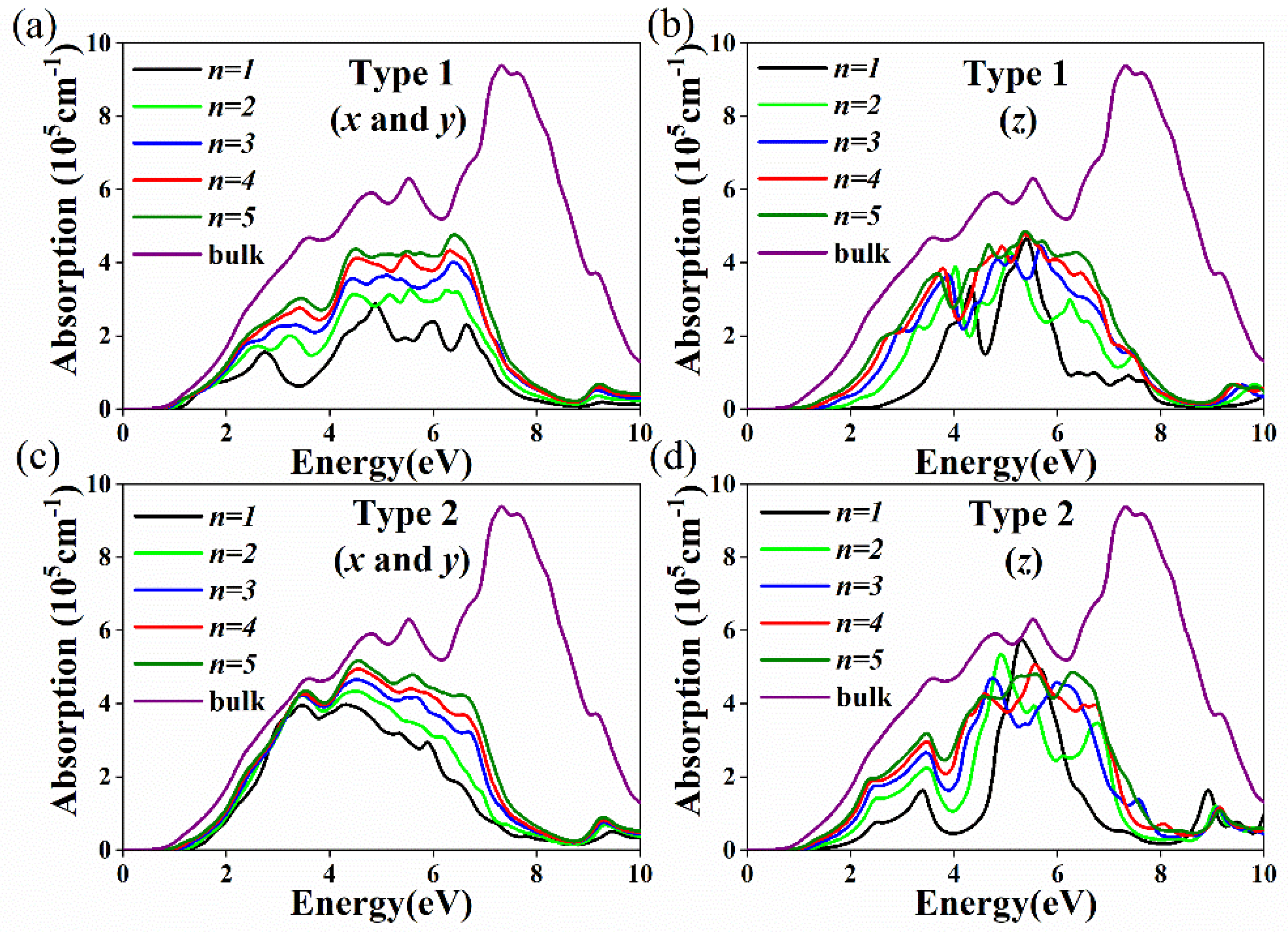
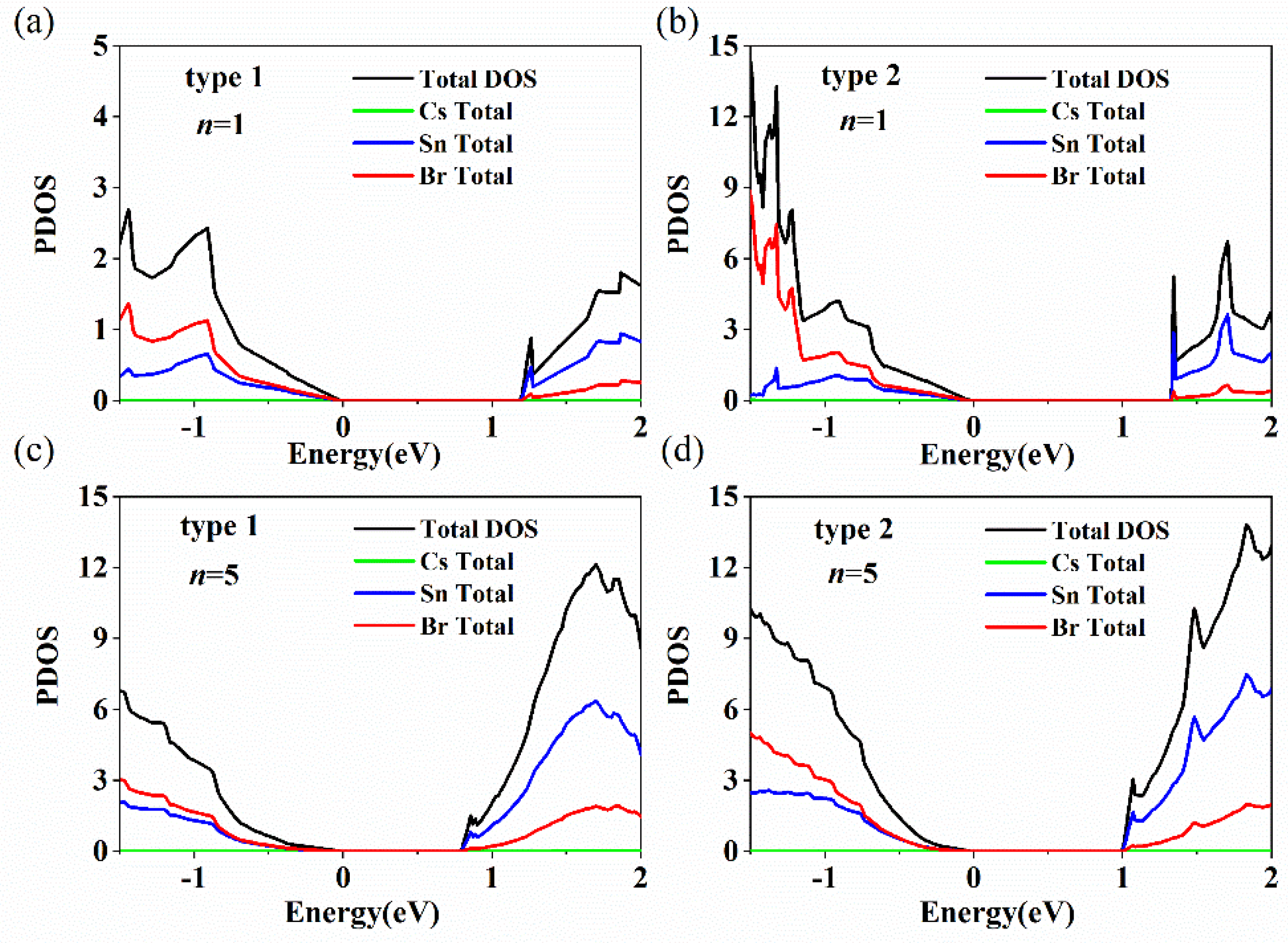
:
1. Introduction
2. Computational Model and Method
3. Results and Discussion
4. Conclusions
Supplementary Materials
Author Contributions
Funding
Data Availability Statement
Conflicts of Interest
References
- Liu, X.K.; Xu, W.; Bai, S.; Jin, Y.; Wang, J.; Friend, R.H.; Gao, F. Metal halide perovskites for light-emitting diodes. Nat. Mater. 2021, 20, 10–21. [Google Scholar] [CrossRef] [PubMed]
- Jia, Y.; Kerner, R.A.; Grede, A.J.; Rand, B.P.; Giebink, N.C. Continuous-wave lasing in an organic-inorganic lead halide semiconductor. Nat. Photonics 2017, 11, 784–788. [Google Scholar] [CrossRef]
- Fu, Y.; Zhu, H.; Stoumpos, C.C.; Ding, Q.; Wang, J.; Kanatzidis, M.G.; Zhu, X.; Jin, S. Broad Wavelength Tunable Robust Lasing from Single-Crystal Nanowires of Cesium Lead Halide Perovskites (CsPbX3, X = Cl, Br, I). ACS Nano 2016, 10, 7963–7972. [Google Scholar] [CrossRef] [PubMed]
- Kim, J.Y.; Lee, J.W.; Jung, H.S.; Shin, H.; Park, N.G. High-Efficiency Perovskite Solar Cells. Chem 2020, 120, 7867–7918. [Google Scholar]
- Lin, K.; Xing, J.; Quan, L.; Arquer, F.P.G.; Gong, X.; Lu, J.; Xie, L.; Zhao, W.; Zhang, D.; Yan, C.; et al. Perovskite light-emitting diodes with external quantum efficiency exceeding 20 per cent. Nature 2018, 562, 245–248. [Google Scholar] [CrossRef]
- Chen, B.; Yu, Z.; Liu, K.; Zheng, X.; Liu, Y.; Shi, J.; Spronk, D.; Rudd, P.N.; Holman, Z.; Huang, J. Grain Engineering for Perovskite/Silicon Monolithic Tandem Solar Cells with Efficiency of 25.4%. Joule 2019, 3, 177–190. [Google Scholar] [CrossRef] [Green Version]
- Turren-Cruz, S.H.; Saliba, M.; Mayer, M.T.; Juárez-Santiesteban, H.; Mathew, X.; Nienhaus, L.; Tress, W.; Erodici, M.P.; Sher, M.J.; Bawendi, M.G.; et al. Enhanced charge carrier mobility and lifetime suppress hysteresis and improve efficiency in planar perovskite solar cells. Energy Environ. Sci. 2018, 11, 78–86. [Google Scholar] [CrossRef]
- Chen, B.; Baek, S.W.; Hou, Y.; Aydin, E.; Bastiani, M.D.; Scheffel, B.; Proppe, A.; Huang, Z.; Wei, M.; Wang, Y.; et al. Enhanced optical path and electron diffusion length enable high-efficiency perovskite tandems. Nat. Commun. 2020, 11, 1257. [Google Scholar] [CrossRef]
- Qiu, X.; Cao, B.; Yuan, S.; Chen, X.; Qiu, Z.; Jiang, Y.; Ye, Q.; Wang, H.; Zeng, H.; Liu, J.; et al. From unstable CsSnI3 to air-stable Cs2SnI6: A lead-free perovskite solar cell light absorber with bandgap of 1.48 eV and high absorption coefficient. Sol. Energy Mater Sol. Cells 2017, 159, 227–234. [Google Scholar] [CrossRef] [Green Version]
- Giorgi, G.; Fujisawa, J.I.; Segawa, H.; Yamashita, K. Small Photocarrier Effective Masses Featuring Ambipolar Transport in Methylammonium Lead Iodide Perovskite: A Density Functional Analysis. J. Phys. Chem. Lett. 2013, 4, 4213–4216. [Google Scholar] [CrossRef]
- Leng, K.; Abdelwahab, I.; Verzhbitskiy, I.; Telychko, M.; Chu, L.; Fu, W.; Chi, X.; Guo, N.; Chen, Z.; Chen, Z.; et al. Molecularly thin two-dimensional hybrid perovskites with tunable optoelectronic properties due to reversible surface relaxation. Nat. Mater. 2018, 17, 908–914. [Google Scholar] [CrossRef]
- Shao, H.; Bai, X.; Cui, H.; Pan, G.; Jing, P.; Qu, S.; Zhu, J.; Zhai, Y.; Dong, B.; Song, H. White light emission in Bi3+/Mn2+ ion co-doped CsPbCl3 perovskite nanocrystals. Nanoscale 2018, 10, 1023–1029. [Google Scholar] [CrossRef]
- Braly, I.L.; Quilettes, D.W.; Pazos-Outón, L.M.; Burke, S.; Ziffer, M.E.; Ginger, D.S.; Hillhouse, H.W. Hybrid perovskite films approaching the radiative limit with over 90% photoluminescence quantum efficiency. Nat. Photonics 2018, 12, 355–361. [Google Scholar] [CrossRef]
- Yang, S.; Chen, S.; Mosconi, E.; Fang, Y.; Xiao, X.; Wang, C.; Zhou, Y.; Yu, Z.; Zhao, J.; Gao, Y.; et al. Stabilizing halide perovskite surfaces for solar cell operation with wide-bandgap lead oxysalts. Science 2019, 365, 473–478. [Google Scholar] [CrossRef] [PubMed] [Green Version]
- Zhou, L.; Guo, X.; Lin, Z.; Ma, J.; Su, J.; Hu, Z.; Zhang, C.; Liu, S.; Chang, J.; Hao, Y. Interface engineering of low temperature processed all-inorganic CsPbI2Br perovskite solar cells toward PCE exceeding 14%. Nano Energy 2019, 60, 583–590. [Google Scholar] [CrossRef]
- Nishimura, K.; Kamarudin, M.A.; Hirotani, D.; Hamada, K.; Shen, Q.; Iikubo, S.; Minemoto, T.; Yoshino, K.; Hayase, S. Lead-free tin-halide perovskite solar cells with 13% efficiency. Nano Energy 2020, 74, 104858. [Google Scholar] [CrossRef]
- Kulbak, M.; Gupta, S.; Kedem, N.; Levine, I.; Bendikov, T.; Hodes, G.; Cahen, D. Cesium Enhances Long-Term Stability of Lead Bromide Perovskite-Based Solar Cells. J. Phys. Chem. Lett. 2016, 7, 167–172. [Google Scholar] [CrossRef] [Green Version]
- Ren, H.; Yu, S.; Chao, L.; Xia, Y.; Sun, Y.; Zuo, S.; Li, F.; Niu, T.; Yang, Y.; Ju, H.; et al. Efficient and stable Ruddlesden-Popper perovskite solar cell with tailored interlayer molecular interaction. Nat. Photonics 2020, 14, 154–163. [Google Scholar] [CrossRef]
- Lai, H.; Kan, B.; Liu, T.; Zheng, N.; Xie, Z.; Zhou, T.; Wan, X.; Zhang, X.; Liu, Y.; Chen, Y. Two-dimensional Ruddlesden-Popper perovskite with nanorod-like morphology for solar cells with efficiency exceeding 15%. J. Am. Chem. Soc. 2018, 140, 11639–11646. [Google Scholar] [CrossRef]
- Li, M.H.; Yeh, H.H.; Chiang, Y.H.; Jeng, U.S.; Su, C.J.; Shiu, H.W.; Hsu, Y.J.; Kosugi, N.; Ohigashi, T.; Chen, Y.A.; et al. Highly Efficient 2D/3D Hybrid Perovskite Solar Cells via Low-Pressure Vapor-Assisted Solution Process. Adv. Mater. 2018, 30, 1801401. [Google Scholar] [CrossRef]
- Liu, B.; Long, M.; Cai, M.; Ding, L.; Yang, J. Interfacial charge behavior modulation in 2D/3D perovskite heterostructure for potential high-performance solar cells. Nano Energy 2019, 59, 715–720. [Google Scholar] [CrossRef]
- Lee, H.D.; Kim, H.; Cho, H.; Cha, W.; Hong, Y.; Kim, Y.H.; Sadhanala, A.; Venugopalan, V.; Kim, J.S.; Choi, J.W.; et al. Efficient Ruddlesden-Popper Perovskite Light-Emitting Diodes with Randomly Oriented Nanocrystals. Adv. Funct. Mater. 2019, 29, 1901225. [Google Scholar] [CrossRef]
- Chinnambedu, R.M.; Chen, T.P.; Li, S.S.; Chen, W.L.; Lo, C.Y.; Liao, Y.M.; Haider, G.; Lin, C.C.; Chen, C.C.; Sankar, R.; et al. Low-Threshold Lasing from 2D Homologous Organic-Inorganic Hybrid Ruddlesden–Popper Perovskite Single Crystals. Nano Lett. 2018, 18, 3221–3228. [Google Scholar]
- Wang, Z.; Lin, Q.; Chmiel, F.P.; Sakai, N.; Herz, L.M.; Snaith, H.J. Efficient ambient-air-stable solar cells with 2D-3D heterostructured butylammonium-caesium-formamidinium lead halide perovskites. Nat. Energy 2017, 2, 17135. [Google Scholar] [CrossRef]
- Katan, C.; Mercier, N.; Even, J. Quantum and Dielectric Confinement Effects in Lower-Dimensional Hybrid Perovskite Semiconductors. Chem. Asian J. 2019, 119, 3140–3192. [Google Scholar] [CrossRef] [PubMed]
- Tsai, H.; Nie, W.; Blancon, J.C.; Stoumpos, C.C.; Asadpour, R.; Harutyunyan, B.; Neukirch, A.J.; Verduzco, R.; Crochet, J.J.; Tretiak, S.; et al. High-efficiency two-dimensional Ruddlesden–Popper perovskite solar cells. Nature 2016, 536, 312–316. [Google Scholar] [CrossRef]
- Zhang, F.; Lu, H.; Tong, J.; Berry, J.J.; Beard, M.C.; Zhu, K. Advances in two-dimensional organic-inorganic hybrid perovskites. Energy Environ. Sci. 2020, 13, 1154–1186. [Google Scholar] [CrossRef]
- Qin, C.; Sandanayaka, A.S.D.; Zhao, C.; Matsushima, T.; Zhang, D.; Fujihara, T.; Adachi, C. Stable room-temperature continuous-wave lasing in quasi-2D perovskite films. Nature 2020, 585, 53–57. [Google Scholar] [CrossRef] [PubMed]
- Mao, L.; Stoumpos, C.C.; Kanatzidis, M.G. Two-Dimensional Hybrid Halide Perovskites: Principles and Promises. J. Am. Chem. Soc. 2019, 141, 1171–1190. [Google Scholar] [CrossRef]
- Vashishtha, P.; Ng, M.; Shivarudraiah, S.B.; Halpert, J.E. High Efficiency Blue and Green Light-Emitting Diodes Using Ruddlesden-Popper Inorganic Mixed alide Perovskites with Butylammonium Interlayers. Chem. Mater. 2018, 31, 83–89. [Google Scholar] [CrossRef] [Green Version]
- Zhou, C.; Lin, H.; He, Q.; Xu, L.; Worku, M.; Chaaban, M.; Lee, S.; Shi, X.; Du, M.; Ma, B. Low dimensional metal halide perovskites and hybrids. Mater. Sci. Eng. R Rep. 2019, 137, 38–65. [Google Scholar] [CrossRef]
- Pramchu, S.; Laosiritaworn, Y.; Jaroenjittichai, A.P. Electronic properties of surface/bulk iodine defects of CsSnBr3 perovskite. Surf. Coat. Technol. 2016, 306, 159–163. [Google Scholar] [CrossRef]
- Brik, M.G.; Ma, C.G.; Krasnenko, V. First-principles calculations of the structural and electronic properties of the cubic CaZrO3 (001) surfaces. Surf. Sci. 2013, 608, 146–153. [Google Scholar] [CrossRef]
- Liu, Q.; Liu, Z.; Chen, J.; Feng, L.; Tian, H.; Zeng, W. Structural and electronic properties of cubic SrHfO3 surface: First principles calculations. Appl. Surf. Sci. 2012, 258, 3455–3461. [Google Scholar] [CrossRef]
- Borstel, G.; Eglitis, R.I.; Kotomin, E.A.; Heifets, E. Modelling of defects and surfaces in perovskite ferroelectrics. Phys. Stat. Sol. 2003, 236, 253–264. [Google Scholar] [CrossRef]
- Cheng, C.; Kunc, K.; Lee, M.H. Structural relaxation and longitudinal dipole moment of SrTiO3 (001) (1×1) surfaces. Phys. Rev. B 2000, 62, 10409–10418. [Google Scholar] [CrossRef]
- Eglitis, R.I. Ab initio calculations of SrTiO3, BaTiO3, PbTiO3, CaTiO3, SrZrO3, PbZrO3 and BaZrO3 (001), (011) and (111) surfaces as well as F centers, polarons, KTN solid solutions and Nb impurities therein. Int. J. Mod. Phys. B 2014, 28, 1430009. [Google Scholar] [CrossRef] [Green Version]
- Padilla, J.; Vanderbilt, D. Ab initio study of SrTiO3 surfaces. Surf. Sci. 1998, 418, 64–70. [Google Scholar] [CrossRef] [Green Version]
- Heifets, E.; Eglitis, R.I.; Kotomin, E.A.; Maier, J.; Borstel, G. Ab initio modeling of surface structure for SrTiO3 perovskite crystals. Phys. Rev. B 2001, 64, 235417. [Google Scholar] [CrossRef] [Green Version]
- Wang, Y.; Arai, M.; Sasaki, T.; Wang, C.; Zhong, W. First-principles study on the (001) surface of cubic PbZrO3 and PbTiO3. Surf. Sci. 2005, 585, 75–84. [Google Scholar] [CrossRef]
- Cohen, B.E.; Wierzbowska, M.; Etgar, L. High Efficiency and High Open Circuit Voltage in Quasi 2D Perovskite Based Solar Cells. Adv. Funct. Mater. 2017, 27, 1604733. [Google Scholar] [CrossRef]
- Cao, D.H.; Stoumpos, C.C.; Farha, O.K.; Hupp, J.T.; Kanatzidis, M.G. 2D Homologous Perovskites as Light-Absorbing Materials for Solar Cell Applications. J. Am. Chem. Soc. 2015, 137, 7843–7850. [Google Scholar] [CrossRef] [PubMed]
- Charlton, G.; Brennan, S.; Muryn, C.A.; McGrath, R.; Norman, D.; Turner, T.S.; Thornton, G. Surface relaxation of SrTiO3 (001). Surf. Sci. 2000, 457, L376–L380. [Google Scholar] [CrossRef]
- Noguera, C. Polar oxide surfaces. J. Phys. Condens. Matter 2000, 12, R367–R410. [Google Scholar] [CrossRef]
- Ikeda, A.; Nishimura, T.; Morishita, T.; Kido, Y. Surface relaxation and rumpling of TiO2-terminated SrTiO3 (001) determined by medium energy ion scattering. Surf. Sci. 1999, 433−435, 520–524. [Google Scholar] [CrossRef]
- Bickel, N.; Schmidt, G.; Heinz, K.; Müller, K. Ferroelectric Relaxation of the SrTi03 (100) Surface. Phys. Rev. Lett. 1989, 62, 2009–2011. [Google Scholar] [CrossRef] [PubMed]
- Ma, C.G.; Krasnenko, V.; Brik, M.G. First-principles calculations of different (001) surface terminations of three cubic perovskites CsCaBr3, CsGeBr3, and CsSnBr3. J. Phys. Chem. Solid 2018, 115, 289–299. [Google Scholar] [CrossRef]
- Runge, E.; Gross, E.K.U. Density-Functional Theory for Time-Dependent Systems. Phys. Rev. Lett. 1984, 52, 997–1000. [Google Scholar] [CrossRef]
- Blochl, P.E. Projector augmented-wave method. Phys. Rev. B 1994, 50, 17953–17979. [Google Scholar] [CrossRef] [Green Version]
- Perdew, J.P.; Burke, K.; Ernzerhof, M. Generalized gradient approximation made simple. Phys. Rev. Lett. 1996, 77, 3865. [Google Scholar] [CrossRef] [Green Version]
- Kresse, G.; Furthmüller, J. Efficient iterative schemes for ab initio total-energy calculations using a plane-wave basis set. Phys. Rev. B 1996, 54, 11169. [Google Scholar] [CrossRef] [PubMed]
- Monkhorst, H.J.; Pack, J.D. Special points for Brillouin-zone integrations. Phys. Rev. B 1976, 13, 5188–5192. [Google Scholar] [CrossRef]
- Bala, A.; Deb, A.K.; Kumar, V. Atomic and Electronic Structure of Two-Dimensional Inorganic Halide Perovskites An+1MnX3n+1 (n = 1−6, A = Cs, M = Pb and Sn, and X = Cl, Br, and I) from ab Initio Calculations. J. Phys. Chem. C 2018, 122, 7464–7473. [Google Scholar] [CrossRef]
- Coduri, M.; Strobel, T.A.; Szafranski, M.; Katrusiak, A.; Mahata, A.; Cova, F.; Bonomi, S.; Mosconi, E.; Angelis, F.D.; Malavasi, L. Band Gap Engineering in MASnBr3 and CsSnBr3 Perovskites: Mechanistic Insights through the Application of Pressure. J. Phys. Chem. Lett. 2019, 10, 7398–7405. [Google Scholar] [CrossRef]
- Grote, C.; Ehrlich, B.; Berger, R.F. Tuning the near-gap electronic structure of tin-halide and lead-halide perovskites via changes in atomic layering. Phys. Rev. B 2014, 90, 205202. [Google Scholar] [CrossRef] [Green Version]
- Liu, B.; Long, M.; Cai, M.; Yang, J. Influence of the number of layers on ultrathin CsSnI3 perovskite: From electronic structure to carrier mobility. J. Phys. D Appl. Phys. 2018, 51, 105101. [Google Scholar] [CrossRef]
- Gao, L.; Tang, Y.; Diao, X. First-Principles Study on the Photoelectric Properties of CsGeI3 under Hydrostatic Pressure. Appl. Sci. 2020, 10, 5055. [Google Scholar] [CrossRef]
- Zhao, Y.; Liu, B.; Yu, Z.; Ma, J.; Wan, Q.; He, P.; Cai, M. Strong ferroelectric polarization of CH3NH3GeI3 with high-absorption and mobility transport anisotropy: Theoretical study. J. Mater. Chem. C 2017, 5, 5356–5364. [Google Scholar] [CrossRef]
- Yu, Z.; Ma, Q.; Liu, B.; Zhao, Y.; Wang, L.; Zhou, H.; Cai, M. Oriented tuning the photovoltaic properties of γ-RbGeX3 by strain-induced electron effective mass mutation. J. Phys. D Appl. Phys. 2017, 50, 465101. [Google Scholar] [CrossRef] [Green Version]


| Layer (n) | 1 | 2 | 3 | 4 | 5 | ||
|---|---|---|---|---|---|---|---|
| δi,i+1 (%) | Type 1 | Br1Sn2 | 0.6 | −1.05 | −1.56 | −1.64 | −1.71 |
| Sn2Br3 | 1.69 | 2.28 | 2.62 | 2.6 | |||
| Br3Sn4 | 0.004 | −0.49 | −0.69 | ||||
| Sn4Br5 | 0.62 | 0.79 | |||||
| Br5Sn6 | 0.02 | ||||||
| Type 2 | Sn1Br2 | −1.98 | −2.68 | −2.87 | −2.9 | −3 | |
| Br2Sn3 | 0.24 | 1.14 | 1.52 | 1.69 | |||
| Sn3Br4 | −0.74 | −1.01 | −1.13 | ||||
| Br4Sn5 | 0.055 | 0.33 | |||||
| Sn5Br6 | −0.25 | ||||||
| ηi (%) | Type 1 | Cs1Br1Cs1 | −6.44 | −8.28 | −8.89 | −8.78 | −8.89 |
| Br2Sn2Br2 | 0 | −1.78 | −1.94 | −1.89 | −1.94 | ||
| Cs3Br3Cs3 | 0 | −2.44 | −3.11 | −3.44 | |||
| Br4Sn4Br4 | 0 | −0.17 | −0.33 | ||||
| Cs5Br5Cs5 | 0 | −0.72 | |||||
| Br6Sn6Br6 | 0 | ||||||
| Type 2 | Br1Sn1Br1 | −3.22 | −3.28 | −3.17 | −2.94 | −2.83 | |
| Cs2Br2Cs2 | 0 | −2.11 | −2.83 | −3.28 | −3.67 | ||
| Br3Sn3Br3 | 0 | −0.078 | −1 | −1 | |||
| Cs4Br4Cs4 | 0 | −0.89 | −1.28 | ||||
| Br5Sn5Br5 | 0 | −0.22 | |||||
| Cs6Br6Cs6 | 0 | ||||||
| Layer (n) | 1 | 2 | 3 | 4 | 5 | Bulk |
|---|---|---|---|---|---|---|
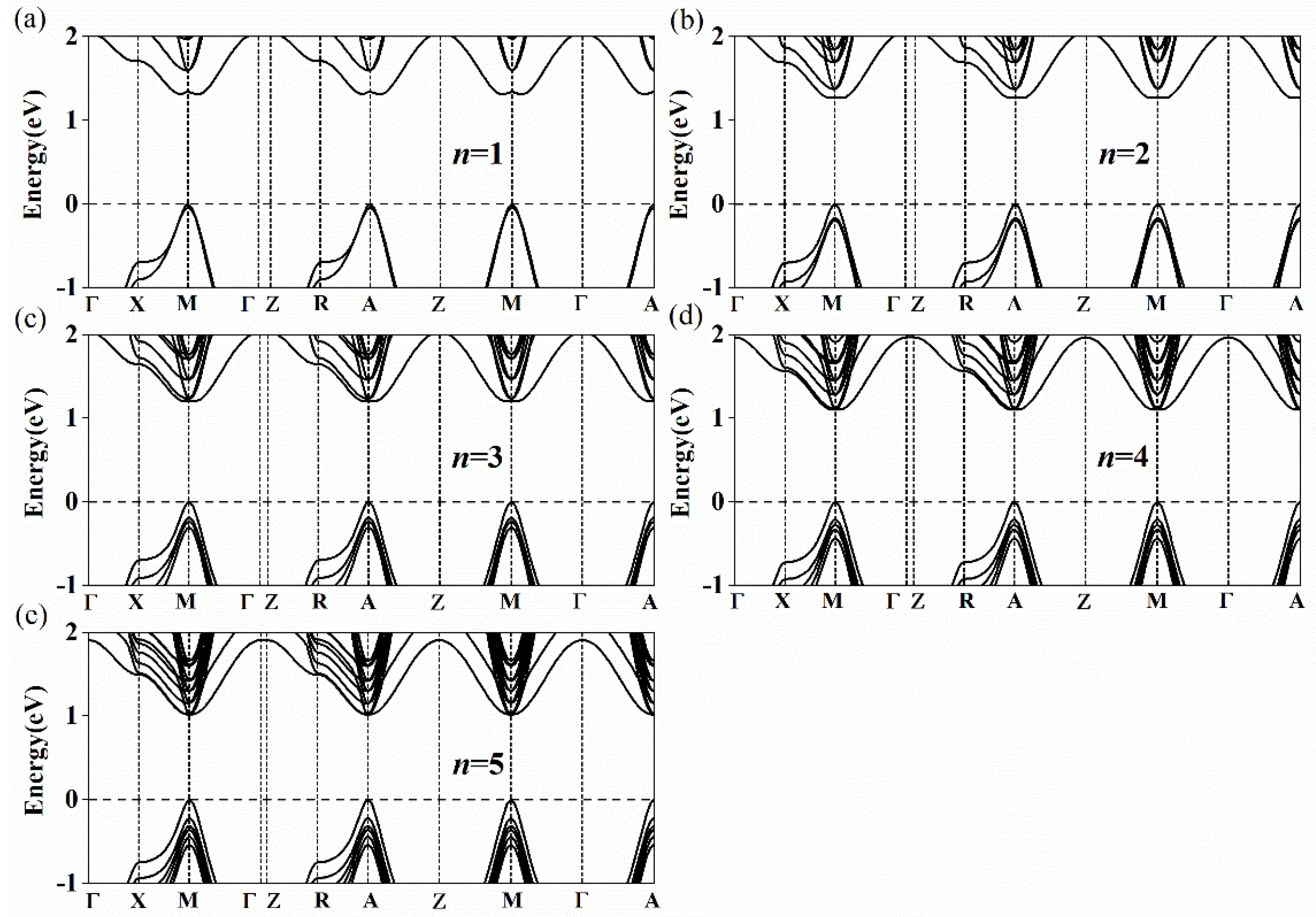
| Type 1 | 1.209 (d) | 1.036 (d) | 0.928 (d) | 0.851 (d) | 0.797 (d) | 0.641 |
| Type 2 | 1.310 (ind) | 1.266 (ind) | 1.198 (ind) | 1.100 (d) | 1.013 (d) |
Publisher’s Note: MDPI stays neutral with regard to jurisdictional claims in published maps and institutional affiliations. |
© 2021 by the authors. Licensee MDPI, Basel, Switzerland. This article is an open access article distributed under the terms and conditions of the Creative Commons Attribution (CC BY) license (https://creativecommons.org/licenses/by/4.0/).
Share and Cite
Xiang, G.; Wu, Y.; Li, Y.; Cheng, C.; Leng, J.; Ma, H. Structural and Optoelectronic Properties of Two-Dimensional Ruddlesden–Popper Hybrid Perovskite CsSnBr3. Nanomaterials 2021, 11, 2119. https://doi.org/10.3390/nano11082119
Xiang G, Wu Y, Li Y, Cheng C, Leng J, Ma H. Structural and Optoelectronic Properties of Two-Dimensional Ruddlesden–Popper Hybrid Perovskite CsSnBr3. Nanomaterials. 2021; 11(8):2119. https://doi.org/10.3390/nano11082119
Chicago/Turabian StyleXiang, Guangbiao, Yanwen Wu, Yushuang Li, Chen Cheng, Jiancai Leng, and Hong Ma. 2021. "Structural and Optoelectronic Properties of Two-Dimensional Ruddlesden–Popper Hybrid Perovskite CsSnBr3" Nanomaterials 11, no. 8: 2119. https://doi.org/10.3390/nano11082119
APA StyleXiang, G., Wu, Y., Li, Y., Cheng, C., Leng, J., & Ma, H. (2021). Structural and Optoelectronic Properties of Two-Dimensional Ruddlesden–Popper Hybrid Perovskite CsSnBr3. Nanomaterials, 11(8), 2119. https://doi.org/10.3390/nano11082119