
Optically Induced Field-Emission Source Based on Aligned Vertical Carbon Nanotube Arrays

Abstract
:1. Introduction
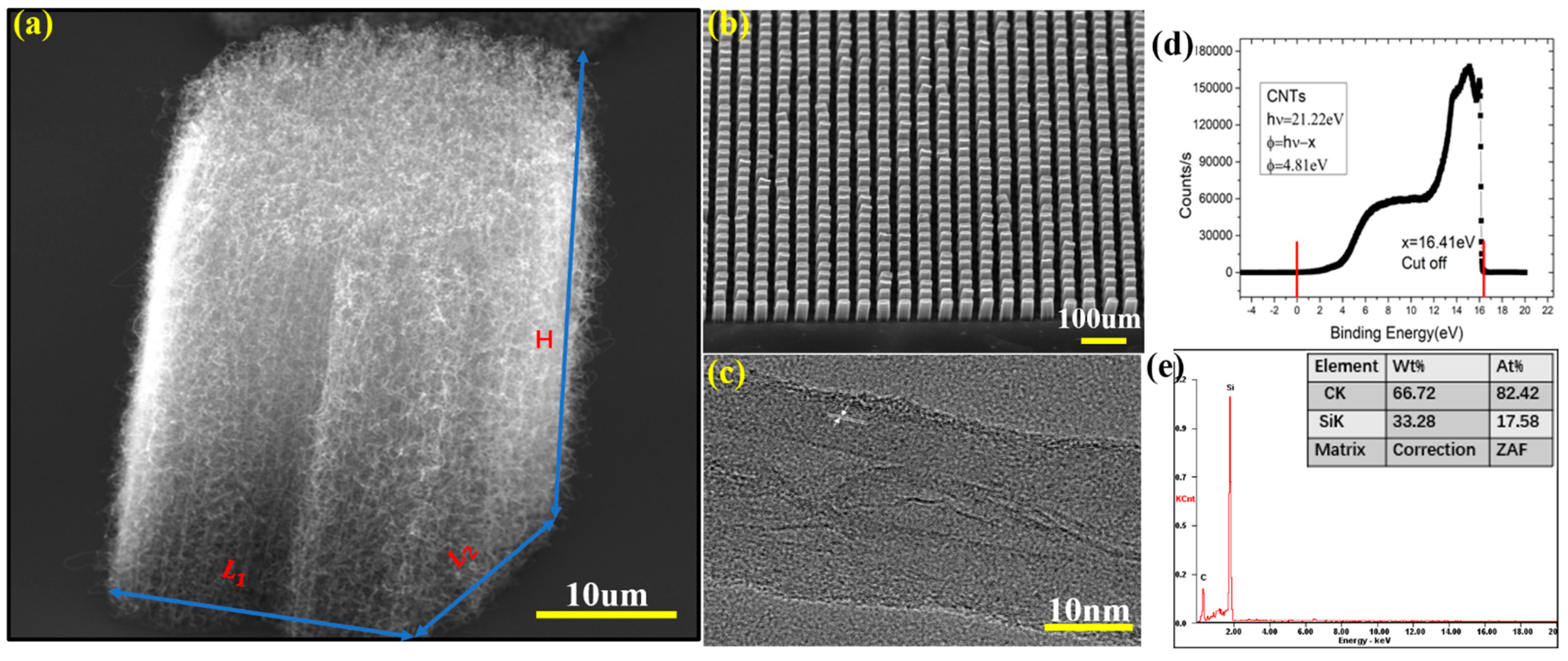
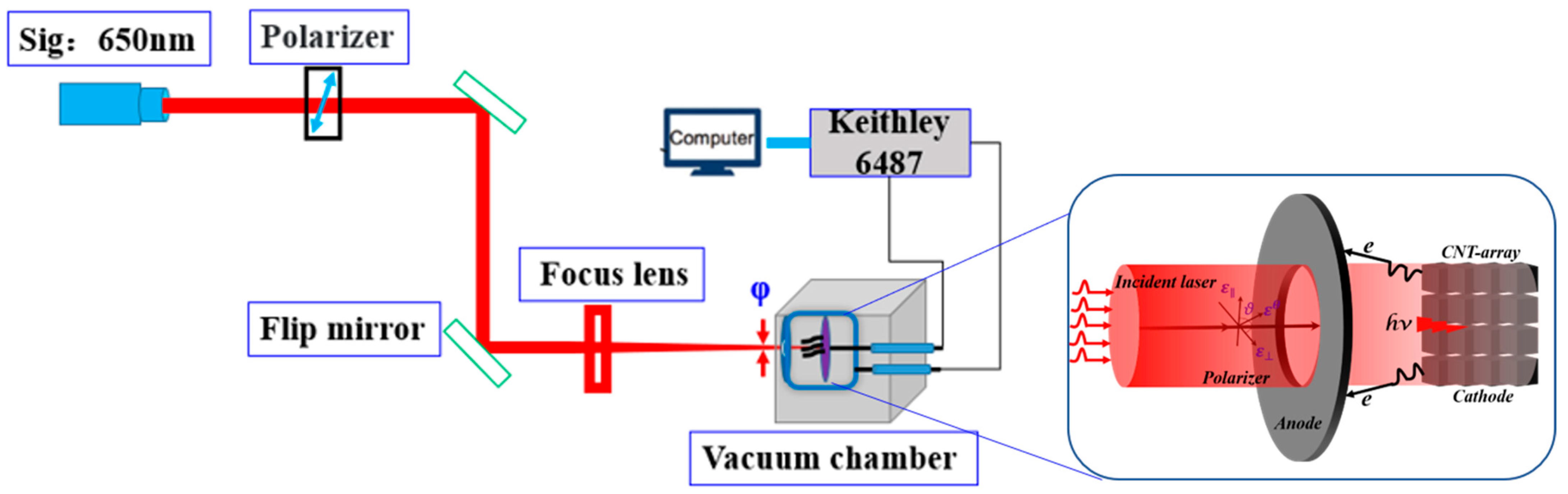
2. Experimental
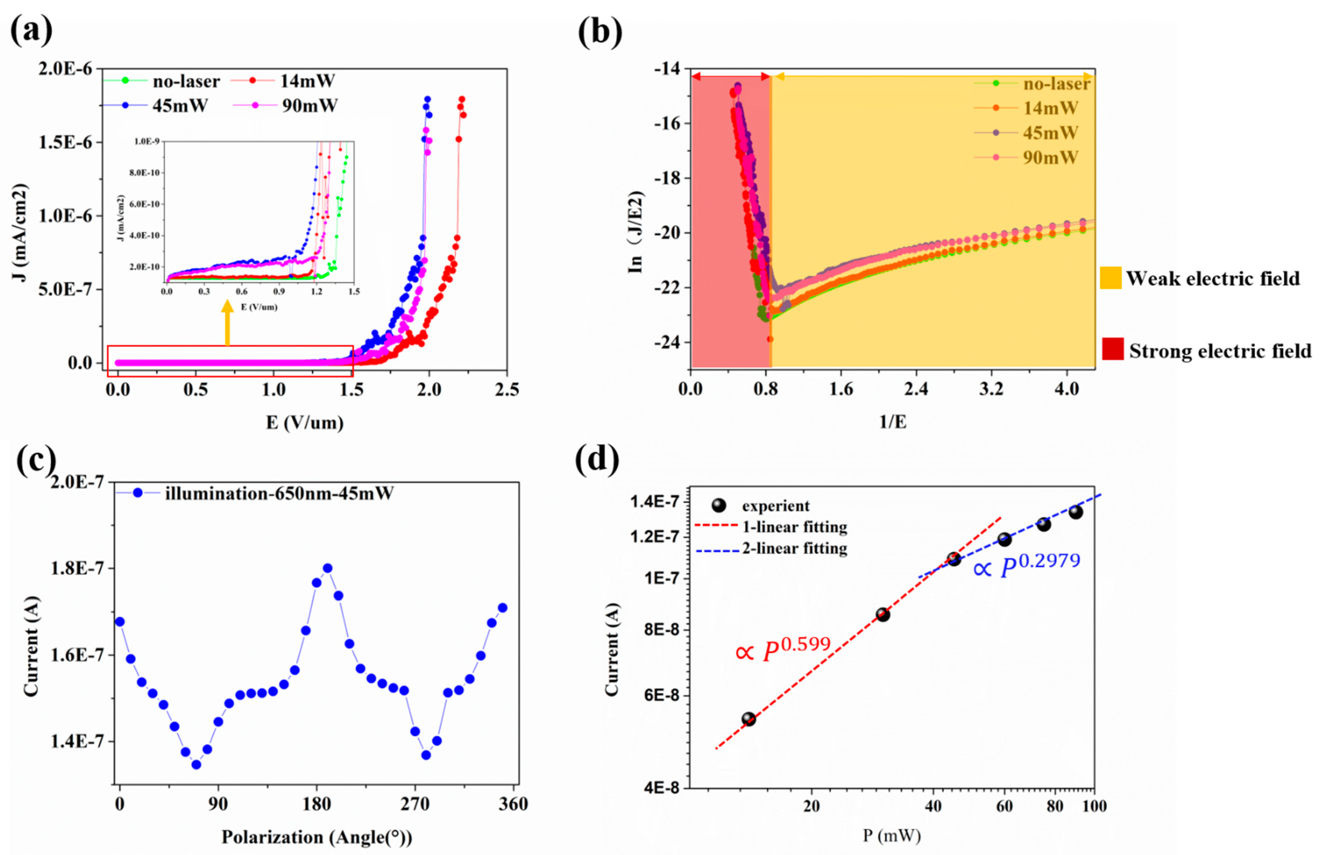
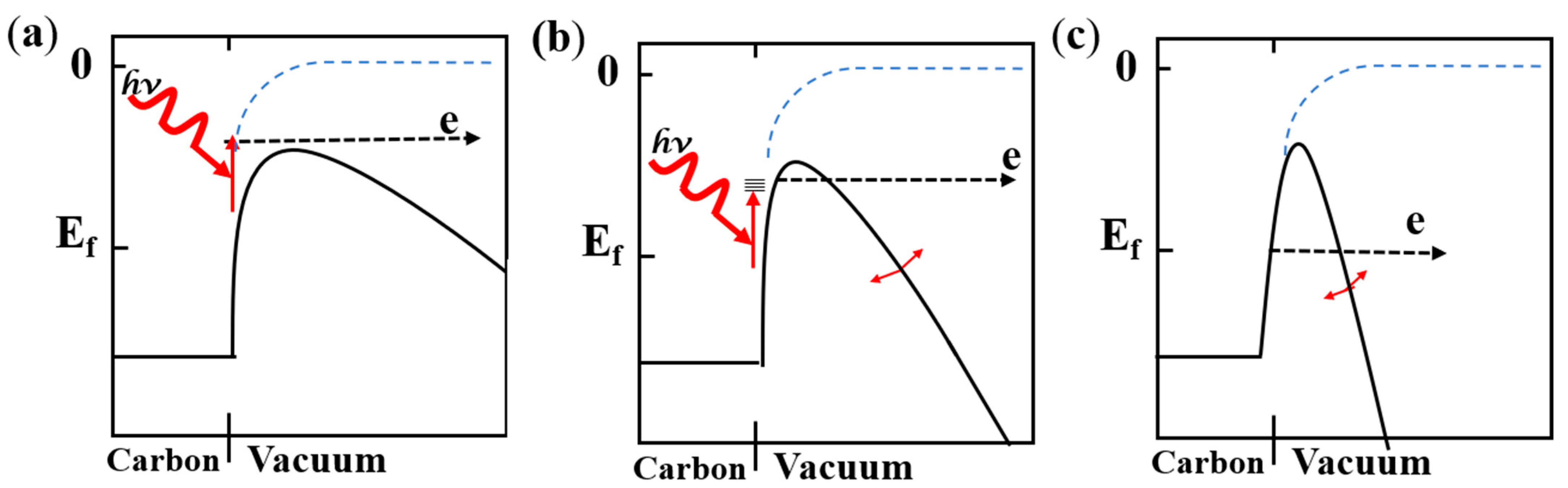
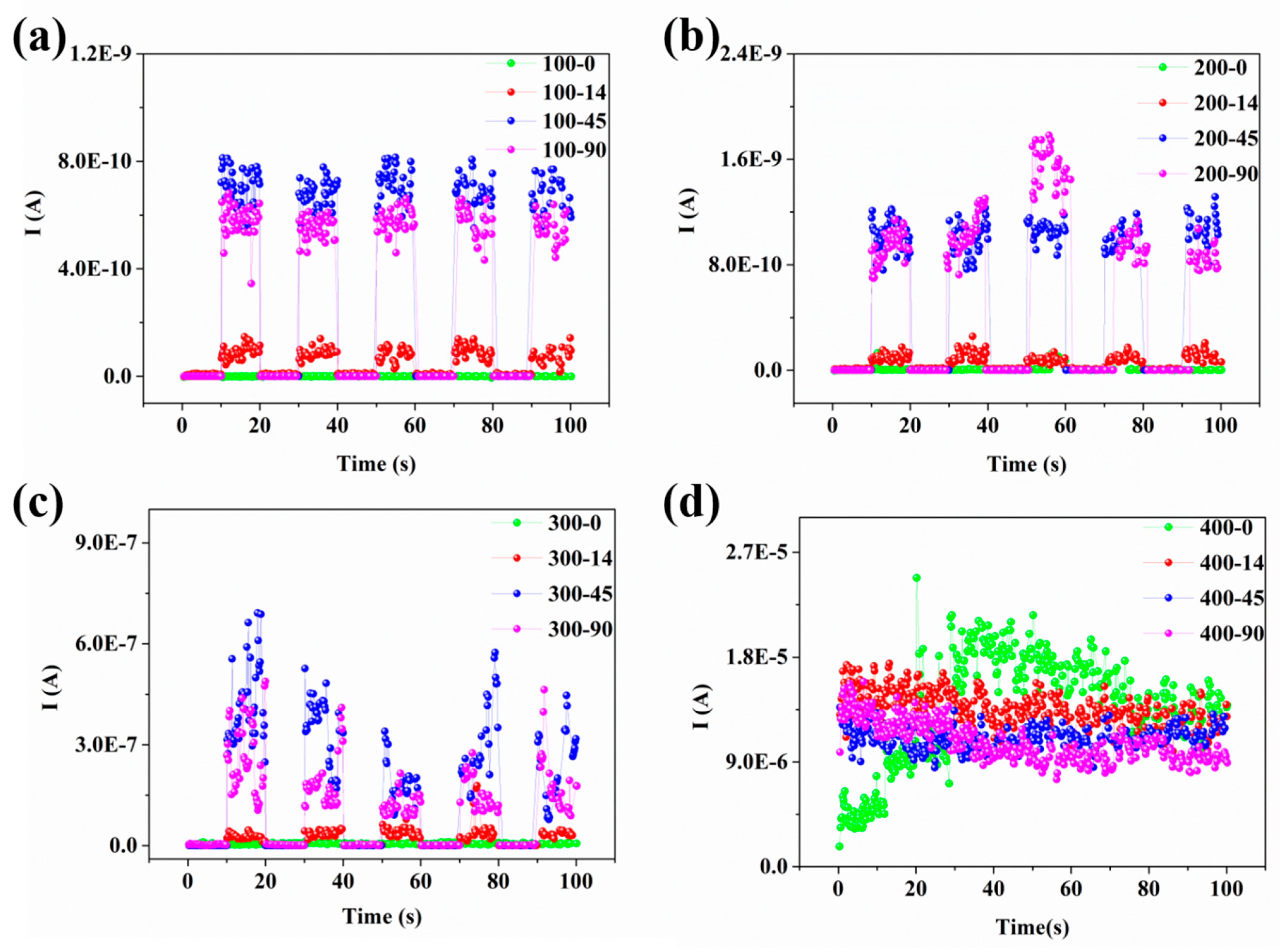
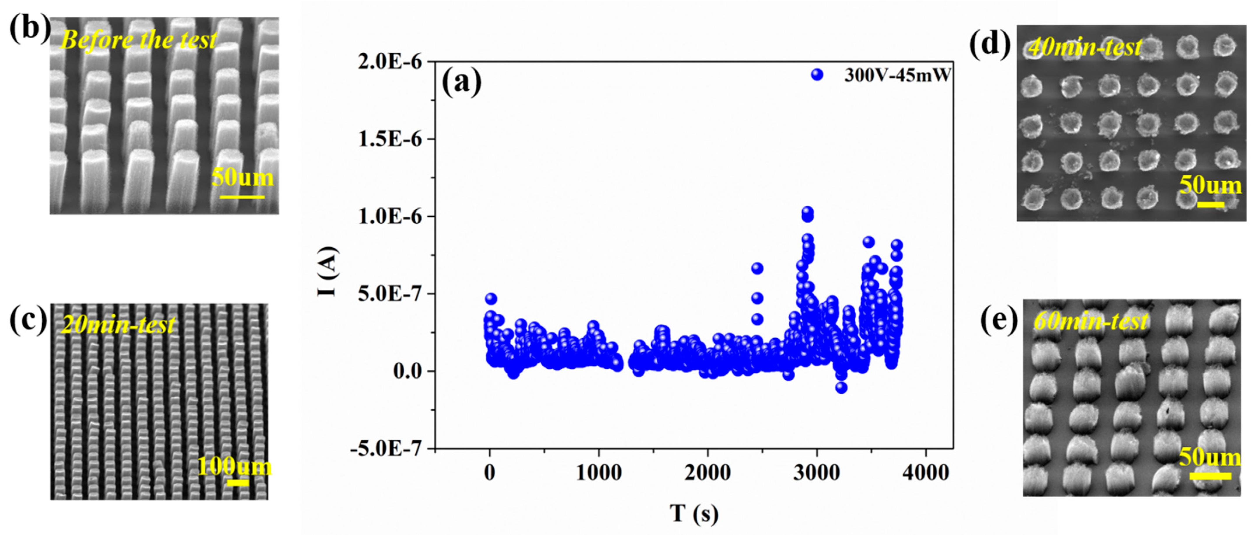
3. Results and Discussion
4. Conclusions
Author Contributions
Funding
Institutional Review Board Statement
Informed Consent Statement
Data Availability Statement
Acknowledgments
Conflicts of Interest
References
- Vanacore, G.M.; Fitzpatrick, A.W.P.; Zewail, A.H. Four-dimensional electron microscopy: Ultrafast imaging, diffraction and spectroscopy in materials science and biology. Nano Today 2016, 11, 228–249. [Google Scholar] [CrossRef] [Green Version]
- Freund, H.P.; Nguyen, D.C.; Carlsten, B. Three-dimensional analysis of prebunched electron beams in an x-ray free-electron laser. Phys. Rev. Spec. Top. Accel. Beams 2012, 15, 030704. [Google Scholar] [CrossRef] [Green Version]
- Gruson, V.; Barreau, L.; Jiménez-Galan, Á.; Risoud, F.; Caillat, J.; Maquet, A.; Carré, B.; Lepetit, F.; Hergott, J.-F.; Ruchon, T.; et al. Attosecond dynamics through a Fano resonance Monitoring the birth of a photoelectron. Science 2016, 354, 734–738. [Google Scholar] [CrossRef] [Green Version]
- Graves, W.S.; Kartner, F.X.; Moncton, D.E.; Piot, P. Intense superradiant x rays from a compact source using a nanocathode array and emittance exchange. Phys. Rev. Lett. 2012, 108, 263904. [Google Scholar] [CrossRef] [PubMed] [Green Version]
- Herink, G.; Solli, D.R.; Gulde, M.; Ropers, C. Field-driven photoemission from nanostructures quenches the quiver motion. Nature 2012, 483, 190–193. [Google Scholar] [CrossRef]
- Kruger, M.; Schenk, M.; Hommelhoff, P. Attosecond control of electrons emitted from a nanoscale metal tip. Nature 2011, 475, 78–81. [Google Scholar] [CrossRef] [PubMed] [Green Version]
- Kasmi, L.; Kreier, D.; Bradler, M.; Riedle, E.; Baum, P. Femtosecond single-electron pulses generated by two-photon photoemission close to the work function. New J. Phys. 2015, 17, 033008. [Google Scholar] [CrossRef] [Green Version]
- Bormann, R.; Gulde, M.; Weismann, A.; Yalunin, S.V.; Ropers, C. Tip-enhanced strong-field photoemission. Phys. Rev. Lett. 2010, 105, 147601. [Google Scholar] [CrossRef]
- Schenk, M.; Kruger, M.; Hommelhoff, P. Strong-field above-threshold photoemission from sharp metal tips. Phys. Rev. Lett. 2010, 105, 257601. [Google Scholar] [CrossRef]
- Feist, A.; Echternkamp, K.E.; Schauss, J.; Yalunin, S.V.; Schafer, S.; Ropers, C. Quantum coherent optical phase modulation in an ultrafast transmission electron microscope. Nature 2015, 521, 200–203. [Google Scholar] [CrossRef]
- Piglosiewicz, B.; Schmidt, S.; Park, D.J.; Vogelsang, J.; Groß, P.; Manzoni, C.; Farinello, P.; Cerullo, G.; Lienau, C. Carrier-envelope phase effects on the strong-field photoemission of electrons from metallic nanostructures. Nat. Photonics 2013, 8, 37–42. [Google Scholar] [CrossRef] [Green Version]
- Kealhofer, C.; Schneider, W.; Ehberger, D.; Ryabov, A.; Krausz, F.; Baum, P. All-optical control and metrology of electron pulses. Science 2016, 352, 429–433. [Google Scholar] [CrossRef] [PubMed]
- Li, Z.; Bai, B.; Li, C.; Dai, Q. Efficient photo-thermionic emission from carbon nanotube arrays. Carbon 2016, 96, 641–646. [Google Scholar] [CrossRef]
- Chen, J.; Yang, B.; Liu, X.; Yang, J.; Cui, L.; Yan, X. Large field emission current and density from robust carbon nanotube cathodes for continuous and pulsed electron sources. Sci. China Mater. 2017, 60, 335–342. [Google Scholar] [CrossRef] [Green Version]
- Chen, J.; Yang, B.; Lim, Y.D.; Su, L.; Yang, J.; Guo, R.; Tay, B.K.; Yan, X. Field emission cathode based on three-dimensional framework carbon and its operation under the driving of a triboelectric nanogenerator. Nano Energy 2018, 49, 308–315. [Google Scholar] [CrossRef]
- Swanwick, M.E.; Keathley, P.D.; Fallahi, A.; Krogen, P.R.; Laurent, G.; Moses, J.; Kartner, F.X.; Velasquez-Garcia, L.F. Nanostructured ultrafast silicon-tip optical field-emitter arrays. Nano Lett. 2014, 14, 5035–5043. [Google Scholar] [CrossRef] [Green Version]
- Velasquez-Garcia, L.F.; Guerrera, S.A.; Niu, Y.; Akinwande, A.I. Uniform High-Current Cathodes Using Massive Arrays of Si Field Emitters Individually Controlled by Vertical Si Ungated FETs—Part 2: Device Fabrication and Characterization. IEEE Trans. Electron. Devices 2011, 58, 1783–1791. [Google Scholar] [CrossRef]
- Nagao, M.; Yasumuro, C.; Taniguchi, M.; Itoh, S.; Kanemaru, S.; Itoh, J. Field emitter array with a memory function for ultrahigh luminance field. J. Vac. Sci. Technol. B 2007, 25, 464–468. [Google Scholar] [CrossRef]
- Yaghoobi, P.; Moghaddam, M.V.; Michan, M.; Nojeh, A. Visible-light induced electron emission from carbon nanotube forests. J. Vac. Sci. Technol. B 2011, 29, 02B104. [Google Scholar] [CrossRef]
- She, J.C.; Xu, N.S.; Deng, S.Z.; Chen, J.; Bishop, H.; Huq, S.E.; Wang, L.; Zhong, D.Y.; Wang, E.G. Vacuum breakdown of carbon-nanotube field emitters on a silicon tip. Appl. Phys. Lett. 2003, 83, 2671–2673. [Google Scholar] [CrossRef]
- Hendrix, R.; Deibel, J.A.; Fairchild, S.B.; Maruyama, B.; Urbas, A.; Walker, M.; Brown, D. Laser Assisted Electron Emission from Free Standing Carbon Nanotube Paper. In CLEO: Applications and Technology; Optical Society of America: Washington, DC, USA, 2015; p. JW2A.53. [Google Scholar]
- Elezzabi, A.Y.; Betz, M.; Green, M.E.; Urbas, A.M.; Her, T.-H.; Kono, J.; Pasquali, M.; Gengler, J.J.; Headrick, R.J.; Bas, D.A. Laser-assisted field emission in single-walled carbon nanotubes. In Ultrafast Phenomena and Nanophotonics XXII; SPIE OPTO: Bellingham, DC, USA, 2018; p. 37. [Google Scholar]
- Li, Z.; Yang, X.; He, F.; Bai, B.; Zhou, H.; Li, C.; Dai, Q. High current field emission from individual non-linear resistor ballasted carbon nanotube cluster array. Carbon 2015, 89, 1–7. [Google Scholar] [CrossRef]
- Javey, A.; Guo, J.; Wang, Q.; Lundstrom, M.; Dai, H. Ballistic carbon nanotube field-effect transistors. Nature 2003, 424, 654–657. [Google Scholar] [CrossRef]
- Li, C.; Zhou, X.; Zhai, F.; Li, Z.; Yao, F.; Qiao, R.; Chen, K.; Yu, D.; Sun, Z.; Liu, K.; et al. Quiver-quenched optical-field-emission from carbon nanotubes. Appl. Phys. Lett. 2017, 111, 133101. [Google Scholar] [CrossRef] [Green Version]
- Gobin, A.M.; Lee, M.H.; Halas, N.J.; James, W.D.; Drezek, R.A.; West, J.L. Near-Infrared Resonant Nanoshells for Combined Optical Imaging and Photothermal Cancer Therapy. Nano Lett. 2007, 7, 1929–1934. [Google Scholar] [CrossRef] [PubMed]
- Grabtchak, S.; Tonkopi, E.; Whelan, W.M. Optical detection of gold nanoparticles in a prostate-shaped porcine phantom. J. Biomed. Opt. 2013, 18, 077005. [Google Scholar] [CrossRef] [PubMed]
- Hikavyy, A.; Clauws, P.; Deferme, W.; Bogdan, G.; Haenen, K.; Nesladek, M. Investigation of hydrogenated CVD diamond films by photo-thermal ionization spectroscopy. Diam. Relat. Mater. 2006, 15, 682–686. [Google Scholar] [CrossRef]
- Hobbs, R.G.; Yang, Y.; Fallahi, A.; Keathley, P.D.; de Leo, E.; Kartner, F.X.; Graves, W.; Berggren, K.K. High-Yield, Ultrafast, SurfacePlasmonEnhanced, Au Nanorod Optical Field Electron Emitter Arrays. ACS Nano 2014, 8, 11474–11482. [Google Scholar] [CrossRef] [PubMed]
- Jung, S.M.; Hahn, J.; Jung, H.Y.; Suh, J.S. Clean Carbon Nanotube Field Emitters Aligned Horizontally. Nano Lett. 2006, 6, 1569–1573. [Google Scholar] [CrossRef]
- Kim, J.W.; Galanzha, E.I.; Shashkov, E.V.; Moon, H.M.; Zharov, V.P. Golden carbon nanotubes as multimodal photoacoustic and photothermal high-contrast molecular agents. Nat. Nanotechnol. 2009, 4, 688–694. [Google Scholar] [CrossRef] [Green Version]
- Li, C.C.; Yin, X.M.; Chen, L.B.; Li, Q.H.; Wang, T.H. High capacity and excellent cycling stability of branched cobalt oxide nanowires as Liinsertion materials. Appl. Phys. Lett. 2010, 97, 043501. [Google Scholar] [CrossRef]
- Westover, T.L.; Franklin, A.D.; Cola, B.A.; Fisher, T.S.; Reifenberger, R.G. Photo- and thermionic emission from potassium-intercalated carbon nanotube arrays. J. Vac. Sci. Technol. B 2010, 28, 423–434. [Google Scholar] [CrossRef] [Green Version]
- Wisitsora-At, A.; Hsu, S.H.; Kang, W.P.; Davidson, J.L.; Tuantranont, A. Advanced nanodiamond emitter with pyramidal tip-on-pole structure for emission self-regulation. J. Vac. Sci. Technol. B 2012, 30, 022204. [Google Scholar] [CrossRef]
- Kusunoki, T.; Hashizume, T.; Kasuya, K.; Arai, N. Stabilization of cold-field-emission current from a CeB6 single-crystal emitter by using a faceted (100) plane. J. Vac. Sci. Technol. B 2020, 39, 013202. [Google Scholar] [CrossRef]
- Dusane, P.R.; Gavhane, D.S.; Kolhe, P.S.; Bankar, P.K.; Thombare, B.R.; Lole, G.S.; Kale, B.B.; More, M.A.; Patil, S.I. Controlled decoration of palladium (Pd) nanoparticles on graphene nanosheets and its superior field emission behavior. Mater. Res. Bull. 2021, 140, 111335. [Google Scholar] [CrossRef]
- Musumeci, P.; Cultrera, L.; Ferrario, M.; Filippetto, D.; Gatti, G.; Gutierrez, M.S.; Moody, J.T.; Moore, N.; Rosenzweig, C.M.S.J.B.; Travish, G.; et al. Multiphoton Photoemission from a Copper Cathode Illuminated by Ultrashort Laser Pulses in an rf Photoinjector. Phys. Rev. Lett. 2010, 104, 084801. [Google Scholar] [CrossRef]
- Hommelhoff, P.; Sortais, Y.; Aghajani-Talesh, A.; Kasevich, M.A. Field emission tip as a nanometer source of free electron femtosecond pulses. Phys. Rev. Lett. 2006, 96, 077401. [Google Scholar] [CrossRef] [Green Version]
- Li, Y.; Kim, W.; Zhang, Y.; Rolandi, M.; Wang, D.; Dai, H. Growth of Single-Walled Carbon Nanotubes from Discrete Catalytic Nanoparticles of Various Sizes. J. Phys. Chem. B 2001, 105, 11424–11431. [Google Scholar] [CrossRef]
- Valfells, A.; Feldman, D.W.; Virgo, M.; O’Shea, P.G.; Lau, Y.Y. Effects of pulse-length and emitter area on virtual cathode formation in electron guns. Phys. Plasmas 2002, 9, 2377–2382. [Google Scholar] [CrossRef]
- Jensen, K.L. Electron emission theory and its application Fowler–Nordheim equation and beyond. J. Vac. Sci. Technol. B 2003, 21, 1528–1544. [Google Scholar] [CrossRef]
- Fowler, R.H. The Analysis of Photoelectric Sensitivity Curves for Clean Metals at Various Temperatures. Phys. Rev. 1931, 38, 45–56. [Google Scholar] [CrossRef]
- Fann, W.S.; Storz, R.; Tom, H.W.; Bokor, J. Electron thermalization in gold. Phys. Rev. B Condens Matter 1992, 46, 13592–13595. [Google Scholar] [CrossRef]
- Barwick, B.; Corder, C.; Strohaber, J.; Chandler-Smith, N.; Uiterwaal, C.; Batelaan, H. Laser-induced ultrafast electron emission from a field emission tip. New J. Phys. 2007, 9, 142. [Google Scholar] [CrossRef]
- DuBridge, L.A. Theory of the Energy Distribution of Photoelectrons. Phys. Rev. 1933, 43, 727–741. [Google Scholar] [CrossRef]
- Zhou, S.; Chen, K.; Cole, M.T.; Li, Z.; Chen, J.; Li, C.; Dai, Q. Ultrafast Field-Emission Electron Sources Based on Nanomaterials. Adv. Mater. 2019, 31, e1805845. [Google Scholar] [CrossRef]
- Li, C.; Zhou, X.; Zhai, F.; Li, Z.; Yao, F.; Qiao, R.; Chen, K.; Cole, M.T.; Yu, D.; Sun, Z.; et al. Carbon Nanotubes as an Ultrafast Emitter with a Narrow Energy Spread at Optical Frequency. Adv. Mater. 2017, 29, 1701580. [Google Scholar] [CrossRef] [Green Version]
- Riffe, D.M.; Wang, X.Y.; Downer, M.C.; Fisher, D.L.; Tajima, T.; Erskine, J.L. Femtosecond thermionic emission from metals in the space-charge-limited regim. J. Opt. Soc. Am. B 1993, 10, 1424–1435. [Google Scholar] [CrossRef] [Green Version]
- Merschdorf, M.; Pfeiffer, W.; Voll, S.; Gerber, G. Electron gas cooling in Ag nanoparticles on graphite. Phys. Rev. B 2003, 68, 155416. [Google Scholar] [CrossRef]
- Hagmann, M.J. Carbon nanotube clusters may give greater output power with large tunable bandwidth from photomixing in laser-assisted field emission. In Proceedings of the 2007 IEEE 20th International Vacuum Nanoelectronics Conference, Chicago, IL, USA, 8–12 July 2007; pp. 50–51. [Google Scholar]
Publisher’s Note: MDPI stays neutral with regard to jurisdictional claims in published maps and institutional affiliations. |
© 2021 by the authors. Licensee MDPI, Basel, Switzerland. This article is an open access article distributed under the terms and conditions of the Creative Commons Attribution (CC BY) license (https://creativecommons.org/licenses/by/4.0/).
Share and Cite
Li, M.; Wang, Q.; Xu, J.; Zhang, J.; Qi, Z.; Zhang, X. Optically Induced Field-Emission Source Based on Aligned Vertical Carbon Nanotube Arrays. Nanomaterials 2021, 11, 1810. https://doi.org/10.3390/nano11071810
Li M, Wang Q, Xu J, Zhang J, Qi Z, Zhang X. Optically Induced Field-Emission Source Based on Aligned Vertical Carbon Nanotube Arrays. Nanomaterials. 2021; 11(7):1810. https://doi.org/10.3390/nano11071810
Chicago/Turabian StyleLi, Mengjie, Qilong Wang, Ji Xu, Jian Zhang, Zhiyang Qi, and Xiaobing Zhang. 2021. "Optically Induced Field-Emission Source Based on Aligned Vertical Carbon Nanotube Arrays" Nanomaterials 11, no. 7: 1810. https://doi.org/10.3390/nano11071810
APA StyleLi, M., Wang, Q., Xu, J., Zhang, J., Qi, Z., & Zhang, X. (2021). Optically Induced Field-Emission Source Based on Aligned Vertical Carbon Nanotube Arrays. Nanomaterials, 11(7), 1810. https://doi.org/10.3390/nano11071810