
Recent Advances in Two-Dimensional Quantum Dots and Their Applications

 ,
,  ,
, 


Abstract
1. Introduction
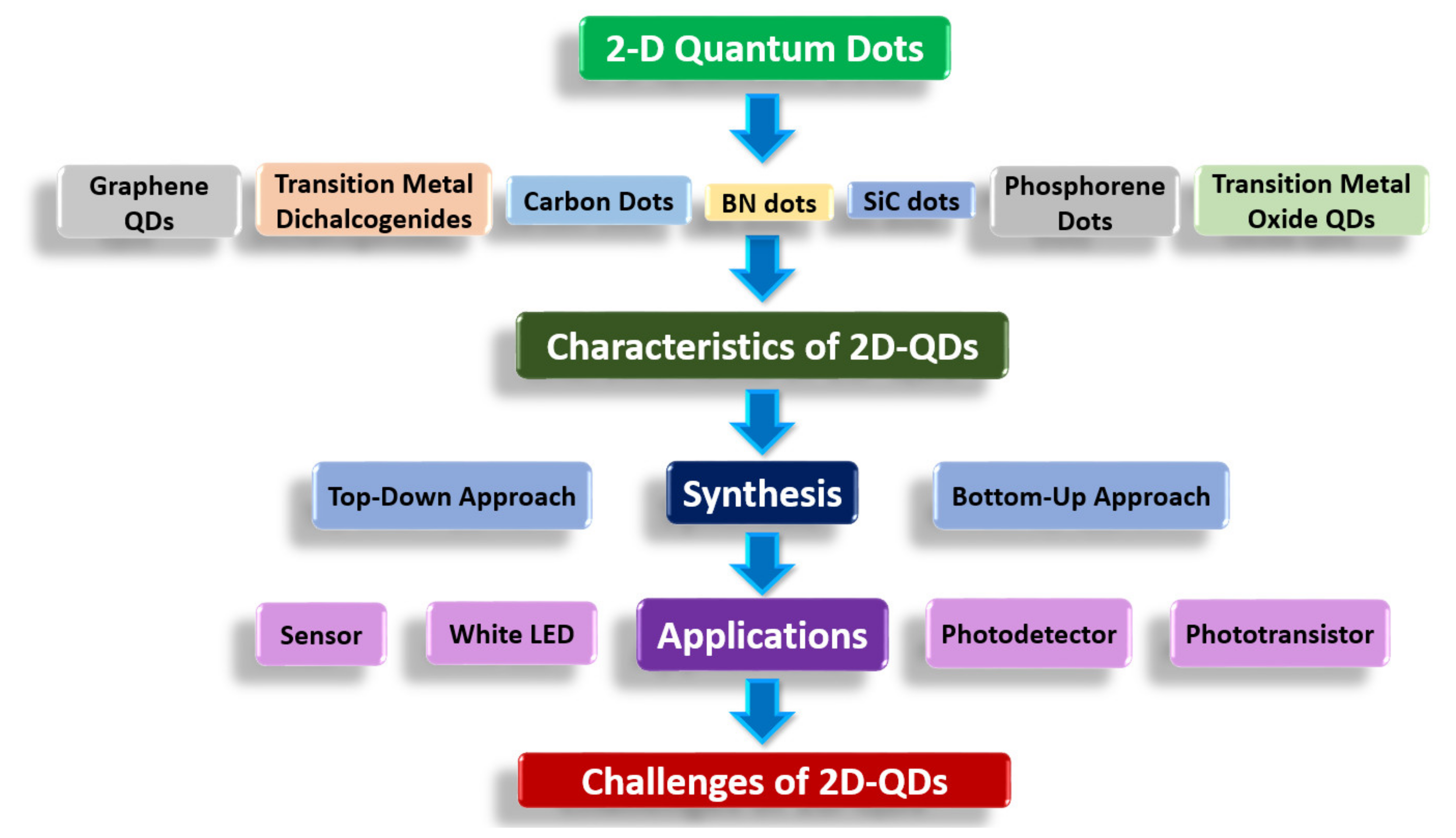
2. Characteristics of 2D-QDs
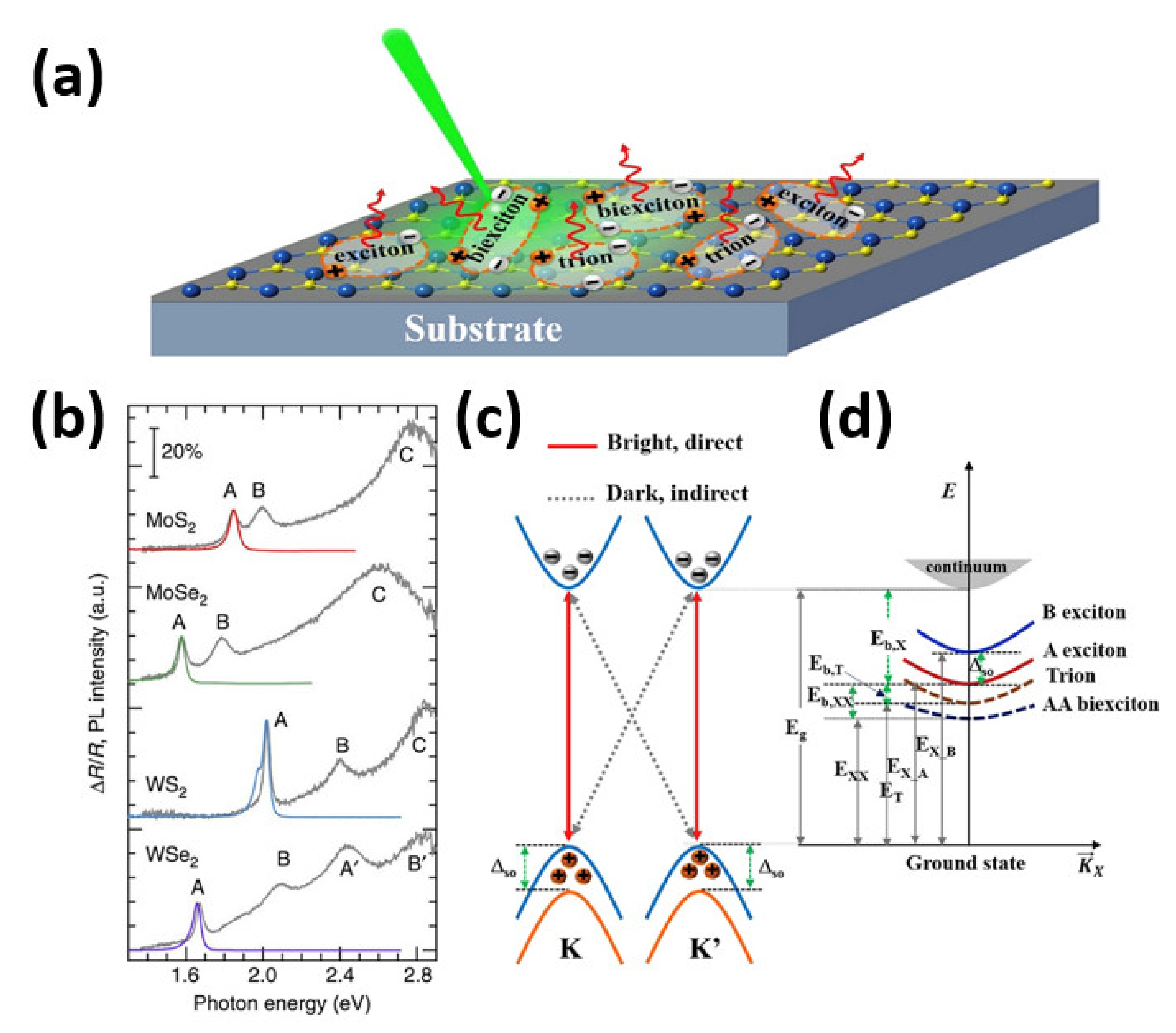
2.1. Excitons in Monolayer TMDs
2.2. Structural and Optical Characteristics of Graphene Quantum Dots (GQDs)
3. Synthesis of 2D-QDs
3.1. Top-down Approaches
3.2. Bottom-up Approaches
4. Hybrid 2D Quantum Dots Materials and Their Applications
5. Challenges Faced by 2D-QDs Materials
5.1. Synthesis/Deposition of 2D-QDs Materials
5.2. Transfer Process
5.3. The Schottky Barrier
6. Conclusions and Future Outlook
Author Contributions
Funding
Institutional Review Board Statement
Informed Consent Statement
Data Availability Statement
Acknowledgments
Conflicts of Interest
References
- Chen, F.; Lin, Q.; Shen, H.; Tang, A. Blue quantum dot-based electroluminescent light-emitting diodes. Mater. Chem. Front. 2020, 4, 1340–1365. [Google Scholar] [CrossRef]
- Motomura, G.; Ogura, K.; Iwasaki, Y.; Nagakubo, J.; Hirakawa, M.; Nishihashi, T.; Tsuzuki, T. Improvement of electroluminescent characteristics in quantum dot light-emitting diodes using ZnInP/ZnSe/ZnS quantum dots by mixing an electron transport material into the light-emitting layer. AIP Adv. 2020, 10, 065228. [Google Scholar] [CrossRef]
- Chen, J.; Hardev, V.; Yurek, J. Quantum-Dot Displays: Giving LCDs a Competitive Edge through Color. Inf. Disp. 2013, 29, 12–17. [Google Scholar] [CrossRef]
- Kumar, D.S.; Kumar, B.J.; Mahesh, H.M. Chapter 3—Quantum Nanostructures (QDs): An Overview. In Synthesis of Inorganic Nanomaterials; Mohan Bhagyaraj, S., Oluwafemi, O.S., Kalarikkal, N., Thomas, S., Eds.; Woodhead Publishing: Sawston, UK, 2018; pp. 59–88. [Google Scholar]
- Ramalingam, G.; Kathirgamanathan, P.; Manivannan, N.; Kasinathan, K. Quantum Confinement Effect of 2D Nanomaterials. In Quantum Dots-Fundamental and Applications; IntechOpen: London, UK, 2020. [Google Scholar]
- Zaini, M.S.; Ying Chyi Liew, J.; Alang Ahmad, S.A.; Mohmad, A.R.; Kamarudin, M.A. Quantum Confinement Effect and Photoenhancement of Photoluminescence of PbS and PbS/MnS Quantum Dots. Appl. Sci. 2020, 10, 6282. [Google Scholar] [CrossRef]
- Cao, F.; Wang, S.; Wang, F.; Wu, Q.; Zhao, D.; Yang, X. A Layer-by-Layer Growth Strategy for Large-Size InP/ZnSe/ZnS Core–Shell Quantum Dots Enabling High-Efficiency Light-Emitting Diodes. Chem. Mater. 2018, 30, 8002–8007. [Google Scholar] [CrossRef]
- Hao, E.; Sun, H.; Zhou, Z.; Liu, J.; Yang, B.; Shen, J. Synthesis and Optical Properties of CdSe and CdSe/CdS Nanoparticles. Chem. Mater. 1999, 11, 3102. [Google Scholar] [CrossRef]
- Loukanov, A.R.; Dushkin, C.D.; Papazova, K.I.; Kirov, A.V.; Abrashev, M.V.; Adachi, E. Photoluminescence depending on the ZnS shell thickness of CdS/ZnS core-shell semiconductor nanoparticles. Colloids Surf. A Physicochem. Eng. Asp. 2004, 245, 9–14. [Google Scholar] [CrossRef]
- Qi, L.; Ma, J.; Cheng, H.; Zhao, Z. Synthesis and characterization of mixed CdS-ZnS nanoparticles in reverse micelles. Colloids Surf. A Physicochem. Eng. Asp. 1996, 111, 195–202. [Google Scholar] [CrossRef]
- Hornyak, G.L.; Dutta, J.; Tibbals, H.F.; Rao, A. Introduction to Nanoscience; CRC Press: Boca Raton, FL, USA, 2008. [Google Scholar]
- Gu, F.; Yang, Z.; Yu, H.; Xu, J.; Wang, P.; Tong, L.; Pan, A. Spatial Bandgap Engineering along Single Alloy Nanowires. J. Am. Chem. Soc. 2011, 133, 2037–2039. [Google Scholar] [CrossRef]
- Chakrabarty, A.; Raffy, G.; Maity, M.; Gartzia-Rivero, L.; Marre, S.; Aymonier, C.; Maitra, U.; Del Guerzo, A. Nanofiber-Directed Anisotropic Self-Assembly of CdSe–CdS Quantum Rods for Linearly Polarized Light Emission Evidenced by Quantum Rod Orientation Microscopy. Small 2018, 14, 1802311. [Google Scholar] [CrossRef]
- Jin, H.; Ahn, M.; Jeong, S.; Han, J.H.; Yoo, D.; Son, D.H.; Cheon, J. Colloidal Single-Layer Quantum Dots with Lateral Confinement Effects on 2D Exciton. J. Am. Chem. Soc. 2016, 138, 13253–13259. [Google Scholar] [CrossRef]
- Manikandan, A.; Chen, Y.Z.; Shen, C.C.; Sher, C.W.; Kuo, H.C.; Chueh, Y.L. A critical review on two-dimensional quantum dots (2D QDs): From synthesis toward applications in energy and optoelectronics. Prog. Quantum Electron. 2019, 68, 100226. [Google Scholar] [CrossRef]
- Xu, Q.; Cai, W.; Li, W.; Sreeprasad, T.S.; He, Z.; Ong, W.J.; Li, N. Two-dimensional quantum dots: Fundamentals, photoluminescence mechanism and their energy and environmental applications. Mater. Today Energy 2018, 10, 222–240. [Google Scholar] [CrossRef]
- Lee, L.; Chen, C.-W.; Manikandan, A.; Lee, S.-H.; Wang, Z.M.; Chueh, Y.-L. Phase-engineered SnSex toward SnSe2/SnSe heterostructure with improved thermal conductance by a low-temperature plasma-assisted chemical vapor reaction. Nano Energy 2018, 44, 419–429. [Google Scholar] [CrossRef]
- Medina, H.; Li, J.G.; Su, T.Y.; Lan, Y.W.; Lee, S.H.; Chen, C.W.; Chen, Y.Z.; Manikandan, A.; Tsai, S.H.; Navabi, A.; et al. Wafer-Scale Growth of WSe2 Monolayers Toward Phase-Engineered Hybrid WOx/WSe2 Films with Sub-ppb NOx Gas Sensing by a Low-Temperature Plasma-Assisted Selenization Process. Chem. Mater. 2017, 29, 1587–1598. [Google Scholar] [CrossRef]
- Manikandan, A.; Lee, L.; Wang, Y.C.; Chen, C.W.; Chen, Y.Z.; Medina, H.; Tseng, J.Y.; Wang, Z.M.; Chueh, Y.L. Graphene-coated copper nanowire networks as a highly stable transparent electrode in harsh environments toward efficient electrocatalytic hydrogen evolution reactions. J. Mater. Chem. A. 2017, 5, 13320–13328. [Google Scholar] [CrossRef]
- Qu, Y.; Medina, H.; Wang, S.W.; Wang, Y.C.; Chen, C.W.; Su, T.Y.; Manikandan, A.; Wang, K.; Shih, Y.C.; Chang, J.W.; et al. Wafer Scale Phase-Engineered 1T- and 2H-MoSe2/Mo Core–Shell 3D-Hierarchical Nanostructures toward Efficient Electrocatalytic Hydrogen Evolution Reaction. Adv. Mater. 2021. [Google Scholar] [CrossRef] [PubMed]
- Sriram, P.; Su, D.S.; Periasamy, A.P.; Manikandan, A.; Wang, S.W.; Chang, H.T.; Chueh, Y.L.; Yen, T.J. Hybridizing Strong Quadrupole Gap Plasmons Using Optimized Nanoantennas with Bilayer MoS2 for Excellent Photo-Electrochemical Hydrogen Evolution. Adv. Energy Mater. 2018, 29, 1801184. [Google Scholar] [CrossRef]
- Hu, S.; Trinchi, A.; Atkin, P.; Cole, I. Tunable Photoluminescence Across the Entire Visible Spectrum from Carbon Dots Excited by White Light. Angew. Chem. Int. Ed. 2015, 54, 2970–2974. [Google Scholar] [CrossRef]
- Liu, M.C.; Xu, Y.; Hu, Y.X.; Yang, Q.Q.; Kong, L.B.; Liu, W.W.; Niu, W.J.; Chueh, Y.L. Electrostatically Charged MoS2/Graphene Oxide Hybrid Composites for Excellent Electrochemical Energy Storage Devices. ACS Appl. Mater. Interfaces 2018, 10, 35571–35579. [Google Scholar] [CrossRef]
- Wang, L.; Li, B.; Xu, F.; Li, Y.; Xu, Z.; Wei, D.; Feng, Y.; Wang, Y.; Jia, D.; Zhou, Y. Visual in vivo degradation of injectable hydrogel by real-time and non-invasive tracking using carbon nanodots as fluorescent indicator. Biomaterials 2017, 145, 192–206. [Google Scholar] [CrossRef]
- Zhu, S.; Meng, Q.; Wang, L.; Zhang, J.; Song, Y.; Jin, H.; Zhang, K.; Sun, H.; Wang, H.; Yang, B. Highly Photoluminescent Carbon Dots for Multicolor Patterning, Sensors, and Bioimaging. Angew. Chem. Int. Ed. 2013, 52, 3953–3957. [Google Scholar] [CrossRef]
- Sun, Z.; Xie, H.; Tang, S.; Yu, X.F.; Guo, Z.; Shao, J.; Zhang, H.; Huang, H.; Wang, H.; Chu, P.K. Ultrasmall Black Phosphorus Quantum Dots: Synthesis and Use as Photothermal Agents. Angew. Chem. Int. Ed. 2015, 54, 11526–11530. [Google Scholar] [CrossRef]
- Li, L.; Lu, S.Z.; Pan, J.; Qin, Z.; Wang, Y.Q.; Wang, Y.; Cao, G.Y.; Du, S.; Gao, H.J. Buckled Germanene Formation on Pt(111). Adv. Mater. 2014, 28, 4820–4824. [Google Scholar] [CrossRef]
- Mannix, A.J.; Zhou, X.F.; Kiraly, B.; Wood, J.D.; Alducin, D.; Myers, B.D.; Liu, X.; Fisher, B.L.; Santiago, U.; Guest, J.R.; et al. Synthesis of borophenes: Anisotropic, two-dimensional boron polymorphs. Science 2015, 350, 1513. [Google Scholar] [CrossRef]
- Vogt, P.; De Padova, P.; Quaresima, C.; Avila, J.; Frantzeskakis, E.; Asensio, M.C.; Resta, A.; Ealet, B.; Le Lay, G. Silicene: Compelling Experimental Evidence for Graphenelike Two-Dimensional Silicon. Phys. Rev. Lett. 2012, 108, 155501. [Google Scholar] [CrossRef]
- Das, S.; Ngashangva, L.; Goswami, P. Carbon Dots: An Emerging Smart Material for Analytical Applications. Micromachines 2021, 12. [Google Scholar] [CrossRef]
- Liu, J.; Li, R.; Yang, B. Carbon Dots: A New Type of Carbon-Based Nanomaterial with Wide Applications. ACS Cent. Sci. 2020, 6, 2179–2195. [Google Scholar] [CrossRef] [PubMed]
- Cho, K.; Yang, J.; Lu, Y. Phosphorene: An emerging 2D material. J. Mater. Res. 2017, 32, 2839–2847. [Google Scholar] [CrossRef]
- Cao, Y.; Dong, H.; Pu, S.; Zhang, X. Photoluminescent two-dimensional SiC quantum dots for cellular imaging and transport. Nano Res. 2018, 11, 4074–4081. [Google Scholar] [CrossRef]
- Kottappara, R.; Palantavida, S.; Vijayan, B.K. Chapter 7—Enhancing semiconductor photocatalysis with carbon nanostructures for water/air purification and self-cleaning applications. In Carbon Based Nanomaterials for Advanced Thermal and Electrochemical Energy Storage and Conversion; Paul, R., Etacheri, V., Wang, Y., Lin, C.-T., Eds.; Elsevier: Amsterdam, The Netherlands, 2019; pp. 139–172. [Google Scholar]
- Khan, K.; Tareen, A.K.; Aslam, M.; Wang, R.; Zhang, Y.; Mahmood, A.; Ouyang, Z.; Zhang, H.; Guo, Z. Recent developments in emerging two-dimensional materials and their applications. J. Mater. Chem. C 2020, 8, 387–440. [Google Scholar] [CrossRef]
- Kormányos, A.; Zólyomi, V.; Drummond, N.D.; Burkard, G. Spin-Orbit Coupling, Quantum Dots, and Qubits in Monolayer Transition Metal Dichalcogenides. Phys. Rev. X 2014, 4, 011034. [Google Scholar] [CrossRef]
- Manzeli, S.; Ovchinnikov, D.; Pasquier, D.; Yazyev, O.V.; Kis, A. 2D transition metal dichalcogenides. Nat. Rev. Mater. 2017, 2, 17033. [Google Scholar] [CrossRef]
- Cheng, H.; Kamegawa, T.; Mori, K.; Yamashita, H. Surfactant-Free Nonaqueous Synthesis of Plasmonic Molybdenum Oxide Nanosheets with Enhanced Catalytic Activity for Hydrogen Generation from Ammonia Borane under Visible Light. Angew. Chem. Int. Ed. 2014, 53, 2910–2914. [Google Scholar] [CrossRef] [PubMed]
- Lin, J.; Zhou, J.; Zuluaga, S.; Yu, P.; Gu, M.; Liu, Z.; Pantelides, S.T.; Suenaga, K. Anisotropic Ordering in 1T′ Molybdenum and Tungsten Ditelluride Layers Alloyed with Sulfur and Selenium. ACS Nano 2018, 12, 894–901. [Google Scholar] [CrossRef]
- Wikipedia, The Free Encyclopedia. Transition Metal Dichalcogenide Monolayers. Available online: https://en.wikipedia.org/w/index.php?title=Transition_metal_dichalcogenide_monolayers&oldid=1027006807 (accessed on 10 June 2021).
- Radisavljevic, B.; Radenovic, A.; Brivio, J.; Giacometti, V.; Kis, A. Single-layer MoS2 transistors. Nat. Nanotechnol. 2011, 6, 147–150. [Google Scholar] [CrossRef]
- Lopez-Sanchez, O.; Lembke, D.; Kayci, M.; Radenovic, A.; Kis, A. Ultrasensitive photodetectors based on monolayer MoS2. Nat. Nanotechnol. 2013, 8, 497–501. [Google Scholar] [CrossRef] [PubMed]
- Shao, B.; Liu, Z.; Zeng, G.; Wang, H.; Liang, Q.; He, Q.; Cheng, M.; Zhou, C.; Jiang, L.; Song, B. Two-dimensional transition metal carbide and nitride (MXene) derived quantum dots (QDs): Synthesis, properties, applications and prospects. J. Mater. Chem. A 2020, 8, 7508–7535. [Google Scholar] [CrossRef]
- Ci, L.; Song, L.; Jin, C.; Jariwala, D.; Wu, D.; Li, Y.; Srivastava, A.; Wang, Z.F.; Storr, K.; Balicas, L.; et al. Atomic layers of hybridized boron nitride and graphene domains. Nat. Mater. 2010, 9, 430–435. [Google Scholar] [CrossRef]
- Gong, Y.; Liu, Z.; Lupini, A.R.; Shi, G.; Lin, J.; Najmaei, S.; Lin, Z.; Elías, A.L.; Berkdemir, A.; You, G.; et al. Band Gap Engineering and Layer-by-Layer Mapping of Selenium-Doped Molybdenum Disulfide. Nano Lett. 2014, 14, 442–449. [Google Scholar] [CrossRef]
- Su, L.; Hei, J.; Wu, X.; Wang, L.; Zhou, Z. Ultrathin Layered Hydroxide Cobalt Acetate Nanoplates Face-to-Face Anchored to Graphene Nanosheets for High-Efficiency Lithium Storage. Adv. Funct. Mater. 2017, 27, 1605544. [Google Scholar] [CrossRef]
- Zhou, J.; Lin, J.; Huang, X.; Zhou, Y.; Chen, Y.; Xia, J.; Wang, H.; Xie, Y.; Yu, H.; Lei, J.; et al. A library of atomically thin metal chalcogenides. Nature 2018, 556, 355–359. [Google Scholar] [CrossRef] [PubMed]
- Kortel, M.; Mansuriya, B.D.; Vargas Santana, N.; Altintas, Z. Graphene Quantum Dots as Flourishing Nanomaterials for Bio-Imaging, Therapy Development, and Micro-Supercapacitors. Micromachines 2020, 11, 866. [Google Scholar] [CrossRef] [PubMed]
- Tajik, S.; Dourandish, Z.; Zhang, K.; Beitollahi, H.; Van Le, Q.; Jang, H.W.; Shokouhimehr, M. Carbon and graphene quantum dots: A review on syntheses, characterization, biological and sensing applications for neurotransmitter determination. RSC Adv. 2020, 10, 15406–15429. [Google Scholar] [CrossRef]
- Zhu, S.; Zhang, J.; Tang, S.; Qiao, C.; Wang, L.; Wang, H.; Liu, X.; Li, B.; Li, Y.; Yu, W.; et al. Surface Chemistry Routes to Modulate the Photoluminescence of Graphene Quantum Dots: From Fluorescence Mechanism to Up-Conversion Bioimaging Applications. Adv. Funct. Mater. 2012, 22, 4732–4740. [Google Scholar] [CrossRef]
- Chien, C.T.; Li, S.S.; Lai, W.J.; Yeh, Y.C.; Chen, H.A.; Chen, I.S.; Chen, L.C.; Chen, K.H.; Nemoto, T.; Isoda, S.; et al. Tunable Photoluminescence from Graphene Oxide. Angew. Chem. Int. Ed. 2012, 51, 6662–6666. [Google Scholar] [CrossRef] [PubMed]
- Zhu, S.; Song, Y.; Zhao, X.; Shao, J.; Zhang, J.; Yang, B. The photoluminescence mechanism in carbon dots (graphene quantum dots, carbon nanodots, and polymer dots): Current state and future perspective. Nano Res. 2015, 8, 355–381. [Google Scholar] [CrossRef]
- Zhu, S.; Wang, L.; Li, B.; Song, Y.; Zhao, X.; Zhang, G.; Zhang, S.; Lu, S.; Zhang, J.; Wang, H.; et al. Investigation of photoluminescence mechanism of graphene quantum dots and evaluation of their assembly into polymer dots. Carbon 2014, 77, 462–472. [Google Scholar] [CrossRef]
- Mukherjee, S.; Maiti, R.; Katiyar, A.K.; Das, S.; Ray, S.K. Novel Colloidal MoS2 Quantum Dot Heterojunctions on Silicon Platforms for Multifunctional Optoelectronic Devices. Sci. Rep. 2016, 6, 29016. [Google Scholar] [CrossRef]
- Yin, W.; Bai, X.; Zhang, X.; Zhang, J.; Gao, X.; Yu, W.W. Light-Emitting Diodes with MoS2 Quantum Dots. Part. Part. Syst. Charact. 2019, 36, 1800362. [Google Scholar] [CrossRef]
- Hu, C.; Dong, D.; Yang, X.; Qiao, K.; Yang, D.; Deng, H.; Yuan, S.; Khan, J.; Lan, Y.; Song, H.; et al. Synergistic Effect of Hybrid PbS Quantum Dots/2D-WSe2 Toward High Performance and Broadband Phototransistors. Adv. Funct. Mater. 2017, 27, 1603605. [Google Scholar] [CrossRef]
- Tang, S.Y.; Yang, C.C.; Su, T.Y.; Yang, T.Y.; Wu, S.C.; Hsu, Y.C.; Chen, Y.Z.; Lin, T.N.; Shen, J.L.; Lin, H.N.; et al. Design of Core–Shell Quantum Dots–3D WS2 Nanowall Hybrid Nanostructures with High-Performance Bifunctional Sensing Applications. ACS Nano 2020, 14, 12668–12678. [Google Scholar] [CrossRef]
- Chang, C.Y.; Yu, C.L.; Lin, C.A.; Lin, H.T.; Lee, A.B.; Chen, Z.Z.; Lu, L.S.; Chang, W.H.; Kuo, H.C.; Shih, M.H. Hybrid Composites of Quantum Dots, Monolayer WSe2, and Ag Nanodisks for White Light-Emitting Diodes. ACS Appl. Nano Mater. 2020, 3, 6855–6862. [Google Scholar] [CrossRef]
- Zeng, H.; Cui, X. An optical spectroscopic study on two-dimensional group-VI transition metal dichalcogenides. Chem. Soc. Rev. 2015, 2629–2642. [Google Scholar] [CrossRef]
- Cheiwchanchamnangij, T.; Lambrecht, W.R.L. Quasiparticle band structure calculation of monolayer, bilayer, and bulk MoS2. Phys. Rev. B 2012, 85, 205302. [Google Scholar] [CrossRef]
- Shi, H.; Pan, H.; Zhang, Y.W.; Yakobson, B.I. Quasiparticle band structures and optical properties of strained monolayer MoS2 and WS2. Phys. Rev. B. 2013, 87, 155304. [Google Scholar] [CrossRef]
- Tran, M.D.; Kim, J.-H.; Lee, Y.H. Tailoring photoluminescence of monolayer transition metal dichalcogenides. Curr. Appl. Phys. 2016, 16, 1159–1174. [Google Scholar] [CrossRef]
- Yu, H.; Cui, X.; Xu, X.; Yao, W. Valley excitons in two-dimensional semiconductors. Natl. Sci. Rev. 2015, 2, 57–70. [Google Scholar] [CrossRef]
- Velizhanin, K.A.; Saxena, A. Excitonic effects in two-dimensional semiconductors: Path integral Monte Carlo approach. Phys. Rev. B. 2015, 92, 195305. [Google Scholar] [CrossRef]
- Hill, H.M.; Rigosi, A.F.; Roquelet, C.; Chernikov, A.; Berkelbach, T.C.; Reichman, D.R.; Hybertsen, M.S.; Brus, L.E.; Heinz, T.F. Observation of Excitonic Rydberg States in Monolayer MoS2 and WS2 by Photoluminescence Excitation Spectroscopy. Nano Lett. 2015, 15, 2992–2997. [Google Scholar] [CrossRef]
- Yang, J.; Lu, T.; Myint, Y.W.; Pei, J.; Macdonald, D.; Zheng, J.C.; Lu, Y. Robust Excitons and Trions in Monolayer MoTe2. ACS Nano 2015, 9, 6603–6609. [Google Scholar] [CrossRef]
- You, Y.; Zhang, X.X.; Berkelbach, T.C.; Hybertsen, M.S.; Reichman, D.R.; Heinz, T.F. Observation of biexcitons in monolayer WSe2. Nat. Phys. 2015, 11, 477–481. [Google Scholar] [CrossRef]
- Zhu, B.; Chen, X.; Cui, X. Exciton Binding Energy of Monolayer WS2. Sci. Rep. 2015, 5, 9218. [Google Scholar] [CrossRef] [PubMed]
- Bonaccorso, F.; Sun, Z.; Hasan, T.A.; Ferrari, A.C. Graphene photonics and optoelectronics. Nat. Photonics 2010, 4, 611–622. [Google Scholar] [CrossRef]
- Han, M.Y.; Özyilmaz, B.; Zhang, Y.; Kim, P. Energy Band-Gap Engineering of Graphene Nanoribbons. Phys. Rev. Lett. 2017, 98, 206805. [Google Scholar] [CrossRef] [PubMed]
- Ponomarenko, L.A.; Schedin, F.; Katsnelson, M.I.; Yang, R.; Hill, E.W.; Novoselov, K.S.; Geim, A.K. Chaotic Dirac Billiard in Graphene Quantum Dots. Science 2008, 320, 356. [Google Scholar] [CrossRef]
- Ritter, K.A.; Lyding, J.W. The influence of edge structure on the electronic properties of graphene quantum dots and nanoribbons. Nature Mater. 2009, 8, 235–242. [Google Scholar] [CrossRef]
- Kim, S.; Hee Shin, D.; Oh Kim, C.; Seok Kang, S.; Min Kim, J.; Choi, S.H.; Jin, L.H.; Cho, Y.H.; Won Hwang, S.; Sone, C. Size-dependent radiative decay processes in graphene quantum dots. Appl. Phys. Lett. 2012, 101, 163103. [Google Scholar] [CrossRef]
- Zarenia, M.; Chaves, A.; Farias, G.A.; Peeters, F.M. Energy levels of triangular and hexagonal graphene quantum dots: A comparative study between the tight-binding and Dirac equation approach. Phys. Rev. B 2011, 84, 245403. [Google Scholar] [CrossRef]
- Ma, W.-L.; Li, S.-S. Electrically controllable energy gaps in graphene quantum dots. Appl. Phys. Lett. 2012, 100, 163109. [Google Scholar] [CrossRef]
- Kim, S.; Hwang, S.W.; Kim, M.K.; Shin, D.Y.; Shin, D.H.; Kim, C.O.; Yang, S.B.; Park, J.H.; Hwang, E.; Choi, S.H.; et al. Anomalous Behaviors of Visible Luminescence from Graphene Quantum Dots: Interplay between Size and Shape. ACS Nano 2012, 6, 8203–8208. [Google Scholar] [CrossRef]
- Lobyshev, V.I.; Shikhlinskaya, R.E.; Ryzhikov, B.D. Experimental evidence for intrinsic luminescence of water. J. Mol. Liq. 1999, 82, 73–81. [Google Scholar] [CrossRef]
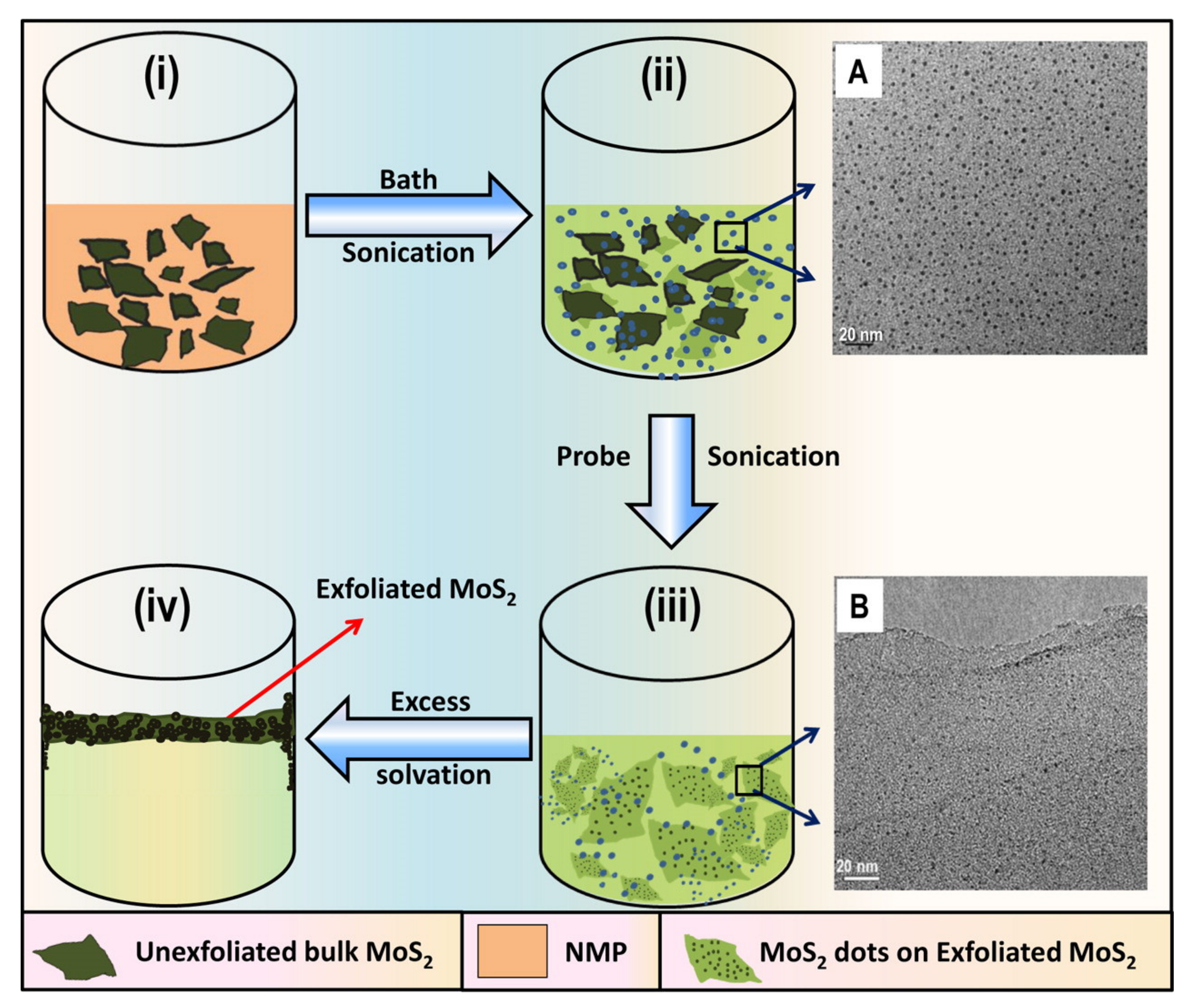
- Qiao, W.; Yan, S.; Song, X.; Zhang, X.; He, X.; Zhong, W.; Du, Y. Luminescent monolayer MoS2 quantum dots produced by multi-exfoliation based on lithium intercalation. Appl. Surf. Sci. 2015, 359, 130–136. [Google Scholar] [CrossRef]
- Gopalakrishnan, D.; Damien, D.; Shaijumon, M.M. MoS2 Quantum Dot-Interspersed Exfoliated MoS2 Nanosheets. ACS Nano 2014, 8, 5297–5303. [Google Scholar] [CrossRef] [PubMed]
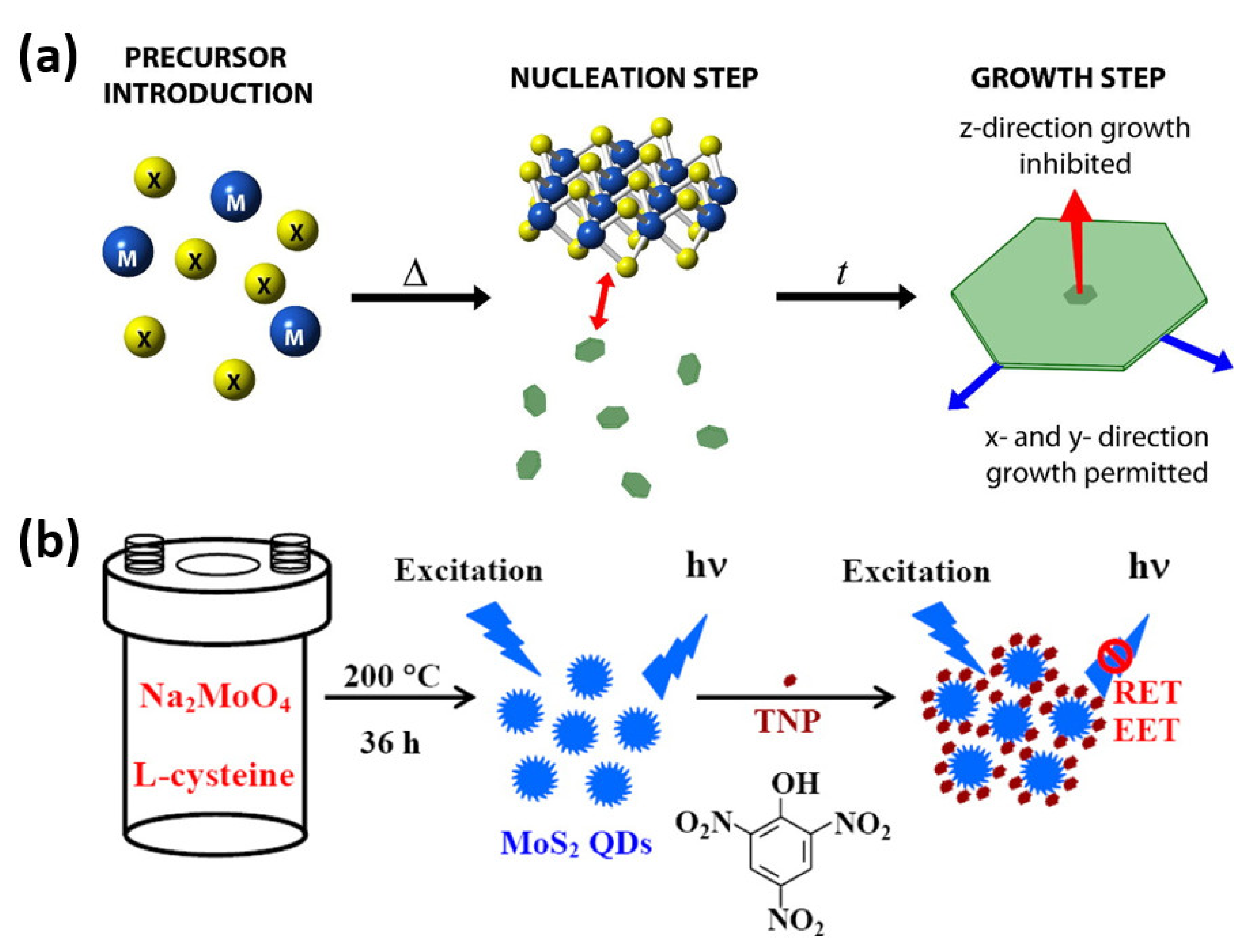
- Pimpinelli, A.; Villain, J. Physics of Crystal Growth; (Collection Alea-Saclay Monographs and Texts in Statistical Physics); Cambridge University Press: Cambridge, UK, 1998. [Google Scholar] [CrossRef]
- Brent, J.R.; Savjani, N.; O’Brien, P. Synthetic approaches to two-dimensional transition metal dichalcogenide nanosheets. Prog. Mater. Sci. 2017, 89, 411–478. [Google Scholar]
- Wang, Y.; Ni, Y. Molybdenum Disulfide Quantum Dots as a Photoluminescence Sensing Platform for 2,4,6-Trinitrophenol Detection. Anal. Chem. 2014, 86, 7463–7470. [Google Scholar] [CrossRef]
- Choi, W.; Choudhary, N.; Han, G.H.; Park, J.; Akinwande, D.; Lee, Y.H. Recent development of two-dimensional transition metal dichalcogenides and their applications. Mater. Today 2017, 20, 116–130. [Google Scholar] [CrossRef]
- Kumar, Y.R.; Deshmukh, K.; Sadasivuni, K.K.; Pasha, S.K. Graphene quantum dot based materials for sensing, bio-imaging and energy storage applications: A review. RSC Adv. 2020, 10, 23861–23898. [Google Scholar] [CrossRef]
- Wang, H.; Yuan, H.; Hong, S.S.; Li, Y.; Cui, Y.H. Physical and chemical tuning of two-dimensional transition metal dichalcogenides. Chem. Soc. Rev. 2015, 44, 2664–2680. [Google Scholar] [CrossRef]
- Choi, W.; Cho, M.Y.; Konar, A.; Lee, J.H.; Cha, G.B.; Hong, S.C.; Kim, S.; Kim, J.; Jena, D.; Joo, J.; et al. High-Detectivity Multilayer MoS2 Phototransistors with Spectral Response from Ultraviolet to Infrared. Adv. Mater. 2012, 24, 5832–5836. [Google Scholar] [CrossRef]
- Duan, X.; Xu, J.; Wei, Z.; Ma, J.; Guo, S.; Liu, H.; Dou, S. Atomically Thin Transition-Metal Dichalcogenides for Electrocatalysis and Energy Storage. Small Methods 2017, 1, 1700156. [Google Scholar] [CrossRef]
- Han, J.K.; Kim, S.; Jang, S.; Lim, Y.R.; Kim, S.W.; Chang, H.; Song, W.; Lee, S.S.; Lim, J.; An, K.S.; et al. Tunable piezoelectric nanogenerators using flexoelectricity of well-ordered hollow 2D MoS2 shells arrays for energy harvesting. Nano Energy 2019, 61, 471–477. [Google Scholar] [CrossRef]
- Huang, H.; Cui, Y.; Li, Q.; Dun, C.; Zhou, W.; Huang, W.; Chen, L.; Hewitt, C.A.; Carroll, D.L. Metallic 1T phase MoS2 nanosheets for high-performance thermoelectric energy harvesting. Nano Energy 2016, 26, 172–179. [Google Scholar] [CrossRef]
- Jariwala, D.; Sangwan, V.K.; Lauhon, L.J.; Marks, T.J.; Hersam, M.C. Emerging Device Applications for Semiconducting Two-Dimensional Transition Metal Dichalcogenides. ACS Nano 2014, 8, 1102–1120. [Google Scholar] [CrossRef] [PubMed]
- Lee, H.S.; Min, S.W.; Chang, Y.G.; Park, M.K.; Nam, T.; Kim, H.; Kim, J.H.; Ryu, S.; Im, S. MoS2 Nanosheet Phototransistors with Thickness-Modulated Optical Energy Gap. Nano Lett. 2012, 12, 3695–3700. [Google Scholar] [CrossRef] [PubMed]
- Lee, H.S.; Min, S.W.; Chang, Y.G.; Park, M.K.; Nam, T.; Kim, H.; Kim, J.H.; Ryu, S.; Im, S. MoS2-Based All-Purpose Fibrous Electrode and Self-Powering Energy Fiber for Efficient Energy Harvesting and Storage. Adv. Energy Mater. 2017, 7, 1601208. [Google Scholar] [CrossRef]
- Long, M.; Wang, P.; Fang, H.; Hu, W. Progress, Challenges, and Opportunities for 2D Material Based Photodetectors. Adv. Funct. Mater. 2019, 29, 1803807. [Google Scholar] [CrossRef]
- Mak, K.F.; Shan, J. Photonics and optoelectronics of 2D semiconductor transition metal dichalcogenides. Nat. Photonics 2016, 10, 216–226. [Google Scholar] [CrossRef]
- Pomerantseva, E.; Gogotsi, Y. Two-dimensional heterostructures for energy storage. Nat. Energy 2017, 2, 17089. [Google Scholar] [CrossRef]
- Shang, J.; Cong, C.; Wu, L.; Huang, W.; Yu, T. Light Sources and Photodetectors Enabled by 2D Semiconductors. Small Methods 2018, 2, 1800019. [Google Scholar] [CrossRef]
- Wang, Q.H.; Kalantar-Zadeh, K.; Kis, A.; Coleman, J.N.; Strano, M.S. Electronics and optoelectronics of two-dimensional transition metal dichalcogenides. Nat. Nanotechnol. 2012, 7, 699–712. [Google Scholar] [CrossRef]
- Chaudhari, A.; Ghoshal, T.; Shaw, M.T.; O’Connell, J.; Kelly, R.A.; Glynn, C.; O’Dwyer, C.; Holmes, J.D.; Morris, M.A. Fabrication of MoS2 Nanowire Arrays and Layered Structures via the Self-Assembly of Block Copolymers. Adv. Mater. Interfaces 2016, 3. [Google Scholar] [CrossRef]
- Han, S.; Luo, X.; Cao, Y.; Yuan, C.; Yang, Y.; Li, Q.; Yu, T.; Ye, S. Morphology evolution of MoS2 nanorods grown by chemical vapor deposition. J. Cryst. Growth 2015, 430, 1–6. [Google Scholar] [CrossRef]
- Jung, Y.; Shen, J.; Liu, Y.; Woods, J.M.; Sun, Y.; Cha, J.J. Metal Seed Layer Thickness-Induced Transition from Vertical to Horizontal Growth of MoS2 and WS2. Nano Lett. 2014, 14, 6842–6849. [Google Scholar] [CrossRef] [PubMed]
- Kong, D.; Wang, H.; Cha, J.J.; Pasta, M.; Koski, K.J.; Yao, J.; Cui, Y. Synthesis of MoS2 and MoSe2 Films with Vertically Aligned Layers. Nano Lett. 2013, 13, 1341–1347. [Google Scholar] [CrossRef]
- Wan, J.; An, B.; Chen, Z.; Zhang, J.; William, W.Y. Nitrogen doped graphene oxide modified WSe2 nanorods for visible light photocatalysis. J. Alloy. Compd. 2018, 750, 499–506. [Google Scholar] [CrossRef]
- Li, B.; Zu, S.; Zhou, J.; Jiang, Q.; Du, B.; Shan, H.; Luo, Y.; Liu, Z.; Zhu, X.; Fang, Z. Single-Nanoparticle Plasmonic Electro—Optic Modulator Based on MoS2 Monolayers. ACS Nano 2017, 11, 9720–9727. [Google Scholar] [CrossRef]
- Li, Y.; DiStefano, J.G.; Murthy, A.A.; Cain, J.D.; Hanson, E.D.; Li, Q.; Castro, F.C.; Chen, X.; Dravid, V.P. Superior Plasmonic Photodetectors Based on Au@MoS2 Core–Shell Heterostructures. ACS Nano 2017, 11, 10321–10329. [Google Scholar] [CrossRef] [PubMed]
- Gough, J.J.; McEvoy, N.; O’Brien, M.; McManus, J.; Garcia-Coindreau, J.; Bell, A.P.; McCloskey, D.; Hrelescu, C.; Duesberg, G.S.; Bradley, A.L. Dependence of Photocurrent Enhancements in Hybrid Quantum Dot-MoS2 Devices on Quantum Dot Emission Wavelength. ACS Photonics 2019, 6, 976–984. [Google Scholar] [CrossRef]
- Gough, J.J.; McEvoy, N.; O’Brien, M.; McManus, J.; Garcia-Coindreau, J.; Bell, A.P.; McCloskey, D.; Hrelescu, C.; Duesberg, G.S.; Bradley, A.L. Dependence of Photocurrent Enhancements in Quantum Dot (QD)-Sensitized MoS2 Devices on MoS2 Film Properties. Adv. Funct. Mater. 2018, 28, 1706149. [Google Scholar] [CrossRef]
- Qin, J.K.; Ren, D.D.; Shao, W.Z.; Li, Y.; Miao, P.; Sun, Z.Y.; Hu, P.; Zhen, L.; Xu, C.Y. Photoresponse Enhancement in Monolayer ReS2 Phototransistor Decorated with CdSe–CdS–ZnS Quantum Dots. ACS Appl. Mater. Interfaces 2017, 9, 39456–39463. [Google Scholar] [CrossRef]
- Zang, H.; Routh, P.K.; Huang, Y.; Chen, J.S.; Sutter, E.; Sutter, P.; Cotlet, M. Nonradiative Energy Transfer from Individual CdSe/ZnS Quantum Dots to Single-Layer and Few-Layer Tin Disulfide. ACS Nano 2016, 10, 4790–4796. [Google Scholar] [CrossRef] [PubMed]
- Hernández-Martínez, P.L.; Govorov, A.O.; Demir, H.V. Förster-Type Nonradiative Energy Transfer for Assemblies of Arrayed Nanostructures: Confinement Dimension vs. Stacking Dimension. J. Phys. Chem. C. 2014, 118, 4951–4958. [Google Scholar] [CrossRef]
- Taghipour, N.; Hernandez Martinez, P.L.; Ozden, A.; Olutas, M.; Dede, D.; Gungor, K.; Erdem, O.; Perkgoz, N.K.; Demir, H.V. Near-Unity Efficiency Energy Transfer from Colloidal Semiconductor Quantum Wells of CdSe/CdS Nanoplatelets to a Monolayer of MoS2. ACS Nano 2018, 12, 8547–8554. [Google Scholar] [CrossRef]
- Li, H.; Zheng, X.; Liu, Y.; Zhang, Z.; Jiang, T. Ultrafast interfacial energy transfer and interlayer excitons in the monolayer WS2/CsPbBr3 quantum dot heterostructure. Nanoscale 2018, 10, 1650–1659. [Google Scholar] [CrossRef]
- Pak, S.; Cho, Y.; Hong, J.; Lee, J.; Lee, S.; Hou, B.; An, G.H.; Lee, Y.W.; Jang, J.E.; Im, H.; et al. Consecutive Junction-Induced Efficient Charge Separation Mechanisms for High-Performance MoS2/Quantum Dot Phototransistors. ACS Appl. Mater. Interfaces 2018, 10, 38264–38271. [Google Scholar] [CrossRef]
- Qin, Y.; Wang, Z.; Liu, D.; Wang, K. Dendritic composite array of silicon nanowires/WO3 nanowires for sensitive detection of NO2 at room temperature. Mater. Lett. 2017, 207, 29–32. [Google Scholar] [CrossRef]
- Zhang, W.; Hu, M.; Liu, X.; Wei, Y.; Li, N.; Qin, Y. Synthesis of the cactus-like silicon nanowires/tungsten oxide nanowires composite for room-temperature NO2 gas sensor. J. Alloys Compd. 2016, 679, 391–399. [Google Scholar] [CrossRef]
- Cheng, R.; Li, D.; Zhou, H.; Wang, C.; Yin, A.; Jiang, S.; Liu, Y.; Chen, Y.; Huang, Y.; Duan, X. Electroluminescence and Photocurrent Generation from Atomically Sharp WSe2/MoS2 Heterojunction p–n Diodes. Nano Lett. 2014, 14, 5590–5597. [Google Scholar] [CrossRef] [PubMed]
- Krasnok, A.; Lepeshov, S.; Alú, A. Nanophotonics with 2D transition metal dichalcogenides [Invited]. Opt. Express 2018, 26, 15972–15994. [Google Scholar] [CrossRef]
- Lien, D.H.; Amani, M.; Desai, S.B.; Ahn, G.H.; Han, K.; He, J.H.; Ager, J.W.; Wu, M.C.; Javey, A. Large-area and bright pulsed electroluminescence in monolayer semiconductors. Nature Commun. 2018, 9, 1229. [Google Scholar] [CrossRef] [PubMed]
- Liu, H.J.; Jiao, L.; Xie, L.; Yang, F.; Chen, J.L.; Ho, W.K.; Gao, C.L.; Jia, J.F.; Cui, X.D.; Xie, M.H. XieMolecular-beam epitaxy of monolayer and bilayer WSe 2: A scanning tunneling microscopy/spectroscopy study and deduction of exciton binding energy. 2D Mater. 2015, 2, 034004. [Google Scholar] [CrossRef]
- Wang, G.; Marie, X.; Gerber, I.; Amand, T.; Lagarde, D.; Bouet, L.; Vidal, M.; Balocchi, A.; Urbaszek, B. Giant Enhancement of the Optical Second-Harmonic Emission of WSe2 Monolayers by Laser Excitation at Exciton Resonances. Phys. Rev. Lett. 2015, 114, 097403. [Google Scholar] [CrossRef] [PubMed]
- Kinkhabwala, A.; Yu, Z.; Fan, S.; Avlasevich, Y.; Müllen, K.; Moerner, W.E. Large single-molecule fluorescence enhancements produced by a bowtie nanoantenna. Nat. Photonics 2009, 3, 654–657. [Google Scholar] [CrossRef]
- Tanaka, K.; Plum, E.; Ou, J.Y.; Uchino, T.; Zheludev, N.I. Multifold Enhancement of Quantum Dot Luminescence in Plasmonic Metamaterials. Phys. Rev. Lett. 2010, 105, 227403. [Google Scholar] [CrossRef]
- Okamoto, K.; Funato, M.; Kawakami, Y.; Tamada, K. High-efficiency light emission by means of exciton–surface-plasmon coupling. J. Photochem. Photobiol. C Photochem. Rev. 2017, 32, 58–77. [Google Scholar] [CrossRef]
- Sun, J.; Hu, H.; Zheng, D.; Zhang, D.; Deng, Q.; Zhang, S.; Xu, H. Light-Emitting Plexciton: Exploiting Plasmon–Exciton Interaction in the Intermediate Coupling Regime. ACS Nano 2018, 12, 10393–10402IN. [Google Scholar] [CrossRef]
- Thomas, R.; Thomas, A.; Pullanchery, S.; Joseph, L.; Somasundaran, S.M.; Swathi, R.S.; Gray, S.K.; Thomas, K.G. Plexcitons: The Role of Oscillator Strengths and Spectral Widths in Determining Strong Coupling. ACS Nano 2018, 12, 402–415. [Google Scholar] [CrossRef]
- Butun, S.; Tongay, S.; Aydin, K. Enhanced Light Emission from Large-Area Monolayer MoS2 Using Plasmonic Nanodisc Arrays. Nano Lett. 2015, 15, 2700–2704. [Google Scholar] [CrossRef]
- Guo, S.; Li, X.; Zhu, J.; Tong, T.; Wei, B. Plasmon-enhanced broadband absorption of MoS2-based structure using Au nanoparticles. Opt. Express 2019, 27, 2305–2316. [Google Scholar]
- Ross, J.S.; Klement, P.; Jones, A.M.; Ghimire, N.J.; Yan, J.; Mandrus, D.G.; Taniguchi, T.; Watanabe, K.; Kitamura, K.; Yao, W.; et al. Electrically tunable excitonic light-emitting diodes based on monolayer WSe2 p-n junctions. Nat. Nanotechnol. 2014, 9, 268–272. [Google Scholar] [CrossRef]
- Konstantatos, G.; Badioli, M.; Gaudreau, L.; Osmond, J.; Bernechea, M.; De Arquer, F.P.G.; Gatti, F.; Koppens, F.H. Hybrid graphene–quantum dot phototransistors with ultrahigh gain. Nat. Nanotechnol. 2012, 7, 363–368. [Google Scholar] [CrossRef] [PubMed]
- Lee, Y.; Kwon, J.; Hwang, E.; Ra, C.H.; Yoo, W.J.; Ahn, J.H.; Park, J.H.; Cho, J.H. High-Performance Perovskite–Graphene Hybrid Photodetector. Adv. Mater. 2015, 27, 41–46. [Google Scholar] [CrossRef] [PubMed]
- Sun, Z.; Liu, Z.; Li, J.; Tai, G.A.; Lau, S.P.; Yan, F. Infrared Photodetectors Based on CVD-Grown Graphene and PbS Quantum Dots with Ultrahigh Responsivity. Adv. Mater. 2012, 24, 5878–5883. [Google Scholar] [CrossRef] [PubMed]
- Xu, H.; Wu, J.; Feng, Q.; Mao, N.; Wang, C.; Zhang, J. High Responsivity and Gate Tunable Graphene-MoS2 Hybrid Phototransistor. Small 2014, 10, 2300–2306. [Google Scholar] [CrossRef] [PubMed]
- Zhang, D.; Gan, L.; Cao, Y.; Wang, Q.; Qi, L.; Guo, X. Understanding Charge Transfer at PbS-Decorated Graphene Surfaces toward a Tunable Photosensor. Adv. Mater. 2012, 24, 2715–2720. [Google Scholar] [CrossRef]
- Kufer, D.; Nikitskiy, I.; Lasanta, T.; Navickaite, G.; Koppens, F.H.; Konstantatos, G. Hybrid 2D–0D MoS2–PbS Quantum Dot Photodetectors. Adv. Mater. 2015, 27, 176–180. [Google Scholar] [CrossRef]
- Koppens, F.H.L.; Mueller, T.; Avouris, P.; Ferrari, A.C.; Vitiello, M.S.; Polini, M. Photodetectors based on graphene, other two-dimensional materials and hybrid systems. Nat. Nanotechnol. 2014, 9, 780–793. [Google Scholar] [CrossRef]
- Li, Y.; Shu, H.; Wang, S.; Wang, J. Electronic and Optical Properties of Graphene Quantum Dots: The Role of Many-Body Effects. J. Phys. Chem. C 2015, 119, 4983–4989. [Google Scholar] [CrossRef]
- Tian, P.; Tang, L.; Teng, K.S.; Lau, S.P. Graphene quantum dots from chemistry to applications. Mater. Today Chem. 2018, 10, 221–258. [Google Scholar] [CrossRef]
- Liu, Y.; Wang, F.; Wang, X.; Wang, X.; Flahaut, E.; Liu, X.; Li, Y.; Wang, X.; Xu, Y.; Shi, Y.; et al. Planar carbon nanotube–graphene hybrid films for high-performance broadband photodetectors. Nat. Commun. 2015, 6, 8589. [Google Scholar] [CrossRef] [PubMed]
- Zhang, W.; Chuu, C.P.; Huang, J.K.; Chen, C.H.; Tsai, M.L.; Chang, Y.H.; Liang, C.T.; Chen, Y.Z.; Chueh, Y.L.; He, J.H.; et al. Ultrahigh-Gain Photodetectors Based on Atomically Thin Graphene-MoS2 Heterostructures. Sci. Rep. 2014, 4, 3826. [Google Scholar] [CrossRef]
- Ma, P.; Salamin, Y.; Baeuerle, B.; Josten, A.; Heni, W.; Emboras, A.; Leuthold, J. Plasmonically Enhanced Graphene Photodetector Featuring 100 Gbit/s Data Reception, High Responsivity, and Compact Size. ACS Photonics. 2019, 6, 154–161. [Google Scholar] [CrossRef]
- Muench, J.E.; Ruocco, A.; Giambra, M.A.; Miseikis, V.; Zhang, D.; Wang, J.; Watson, H.F.; Park, G.C.; Akhavan, S.; Sorianello, V.; et al. Waveguide-Integrated, Plasmonic Enhanced Graphene Photodetectors. Nano Lett. 2019, 19, 7632–7644. [Google Scholar] [CrossRef] [PubMed]
- Schuler, S.; Schall, D.; Neumaier, D.; Dobusch, L.; Bethge, O.; Schwarz, B.; Krall, M.; Mueller, T. Controlled Generation of a p–n Junction in a Waveguide Integrated Graphene Photodetector. Nano Lett. 2016, 16, 7107–7112. [Google Scholar] [CrossRef]
- Schuler, S.; Schall, D.; Neumaier, D.; Schwarz, B.; Watanabe, K.; Taniguchi, T.; Mueller, T. Graphene Photodetector Integrated on a Photonic Crystal Defect Waveguide. ACS Photonics 2018, 5, 4758–4763. [Google Scholar] [CrossRef]
- Shautsova, V.; Sidiropoulos, T.; Xiao, X.; Güsken, N.A.; Black, N.C.; Gilbertson, A.M.; Giannini, V.; Maier, S.A.; Cohen, L.F.; Oulton, R.F. Plasmon induced thermoelectric effect in graphene. Nat. Commun. 2018, 9, 5190. [Google Scholar] [CrossRef] [PubMed]
- Wang, J.; Cheng, Z.; Chen, Z.; Wan, X.; Zhu, B.; Tsang, H.K.; Shu, C.; Xu, J. High-responsivity graphene-on-silicon slot waveguide photodetectors. Nanoscale 2016, 8, 13206–13211. [Google Scholar] [CrossRef]
- Nikitskiy, I.; Goossens, S.; Kufer, D.; Lasanta, T.; Navickaite, G.; Koppens, F.H.; Konstantatos, G. Integrating an electrically active colloidal quantum dot photodiode with a graphene phototransistor. Nat. Commun. 2016, 7, 11954. [Google Scholar] [CrossRef]
- Min, M.; Sakri, S.; Saenz, G.A.; Kaul, A.B. Photophysical Dynamics in Semiconducting Graphene Quantum Dots Integrated with 2D MoS2 for Optical Enhancement in the Near UV. ACS Appl. Mater. Interfaces 2021, 13, 5379–5389. [Google Scholar] [CrossRef]
- Chen, C.; Qiao, H.; Lin, S.; Luk, C.M.; Liu, Y.; Xu, Z.; Song, J.; Xue, Y.; Li, D.; Yuan, J.; et al. Highly responsive MoS2 photodetectors enhanced by graphene quantum dots. Sci. Rep. 2015, 5, 11830. [Google Scholar] [CrossRef] [PubMed]
- Radisavljevic, B.; Kis, A. Mobility engineering and a metal–insulator transition in monolayer MoS2. Nat. Mater. 2013, 12, 815–820. [Google Scholar] [CrossRef] [PubMed]
- Elías, A.L.; Perea-López, N.; Castro-Beltrán, A.; Berkdemir, A.; Lv, R.; Feng, S.; Long, A.D.; Hayashi, T.; Kim, Y.A.; Endo, M.; et al. Controlled Synthesis and Transfer of Large-Area WS2 Sheets: From Single Layer to Few Layers. ACS Nano 2013, 7, 5235–5242. [Google Scholar] [CrossRef] [PubMed]
- Kuc, A.; Zibouche, N.; Heine, T. Influence of quantum confinement on the electronic structure of the transition metal sulfide TS2}. Phys. Rev. B 2011, 83, 245213. [Google Scholar] [CrossRef]
- Cui, Y.; Xin, R.; Yu, Z.; Pan, Y.; Ong, Z.Y.; Wei, X.; Wang, J.; Nan, H.; Ni, Z.; Wu, Y.; et al. High-Performance Monolayer WS2 Field-Effect Transistors on High-κ Dielectrics. Adv. Mater. 2015, 27, 5230–5234. [Google Scholar] [CrossRef] [PubMed]
- Cui, Y.; Xin, R.; Yu, Z.; Pan, Y.; Ong, Z.Y.; Wei, X.; Wang, J.; Nan, H.; Ni, Z.; Wu, Y.; et al. Optical control of charged exciton states in tungsten disulfide. Appl. Phys. Lett. 2015, 106, 201907. [Google Scholar]
- Scrace, T.; Tsai, Y.; Barman, B.; Schweidenback, L.; Petrou, A.; Kioseoglou, G.; Ozfidan, I.; Korkusinski, M.; Hawrylak, P. Magnetoluminescence and valley polarized state of a two-dimensional electron gas in WS2 monolayers. Nat. Nanotechnol. 2015, 10, 603–607. [Google Scholar]
- Zhang, K.; Fu, L.; Zhang, W.; Pan, H.; Sun, Y.; Ge, C.; Du, Y.; Tang, N. Ultrasmall and Monolayered Tungsten Dichalcogenide Quantum Dots with Giant Spin–Valley Coupling and Purple Luminescence. ACS Omega 2018, 3, 12188–12194. [Google Scholar] [CrossRef]
- Dong, R.; Zhang, T.; Feng, X. Interface-Assisted Synthesis of 2D Materials: Trend and Challenges. Chem. Rev. 2018, 118, 6189–6235. [Google Scholar] [CrossRef]
- Sahabudeen, H.; Qi, H.; Glatz, B.A.; Tranca, D.; Dong, R.; Hou, Y.; Zhang, T.; Kuttner, C.; Lehnert, T.; Seifert, G.; et al. Wafer-sized multifunctional polyimine-based two-dimensional conjugated polymers with high mechanical stiffness. Nat. Commun. 2016, 7, 13461. [Google Scholar] [CrossRef]
- Kim, C.; Yoon, M.A.; Jang, B.; Kim, J.H.; Kim, K.S. A Review on Transfer Process of Two-dimensional Materials, (in Ko). Tribol. Lubr. 2020, 36, 1–10. [Google Scholar]
- Li, X.; Zhu, Y.; Cai, W.; Borysiak, M.; Han, B.; Chen, D.; Piner, R.D.; Colombo, L.; Ruoff, R.S. Transfer of Large-Area Graphene Films for High-Performance Transparent Conductive Electrodes. Nano Lett. 2009, 9, 4359–4363. [Google Scholar] [CrossRef] [PubMed]
- Shinde, S.M.; Das, T.; Hoang, A.T.; Sharma, B.K.; Chen, X.; Ahn, J.H. Surface-Functionalization-Mediated Direct Transfer of Molybdenum Disulfide for Large-Area Flexible Devices. Adv. Funct. Mater. 2018, 28, 1706231. [Google Scholar] [CrossRef]
- Park, H.; Brown, P.R.; Bulović, V.; Kong, J. Graphene as Transparent Conducting Electrodes in Organic Photovoltaics: Studies in Graphene Morphology, Hole Transporting Layers, and Counter Electrodes. Nano Lett. 2012, 12, 133–140. [Google Scholar] [CrossRef] [PubMed]
- Xu, Y.; Cheng, C.; Du, S.; Yang, J.; Yu, B.; Luo, J.; Yin, W.; Li, E.; Dong, S.; Ye, P.; et al. Contacts between Two- and Three-Dimensional Materials: Ohmic, Schottky, and p–n Heterojunctions. ACS Nano 2016, 10, 4895–4919. [Google Scholar] [CrossRef]
- Liu, W.; Sarkar, D.; Kang, J.; Cao, W.; Banerjee, K. Impact of Contact on the Operation and Performance of Back-Gated Monolayer MoS2 Field-Effect-Transistors. ACS Nano 2015, 9, 7904–7912. [Google Scholar] [CrossRef] [PubMed]
- Zhou, W.; Guo, Y.; Liu, J.; Wang, F.Q.; Li, X.; Wang, Q. 2D SnSe-based vdW heterojunctions: Tuning the Schottky barrier by reducing Fermi level pinning. Nanoscale 2018, 10, 13767–13772. [Google Scholar] [CrossRef] [PubMed]


| Device Structure | Performance | References |
|---|---|---|
| Core-shell QDs/WS2 hybrid device for gas sensing | The hybrid device demonstrates an outstanding NO2 gas-sensing performance with a remarkably quick response time of 26.8 s to achieve the outstanding gas response efficiency of 95.7%. | [57] |
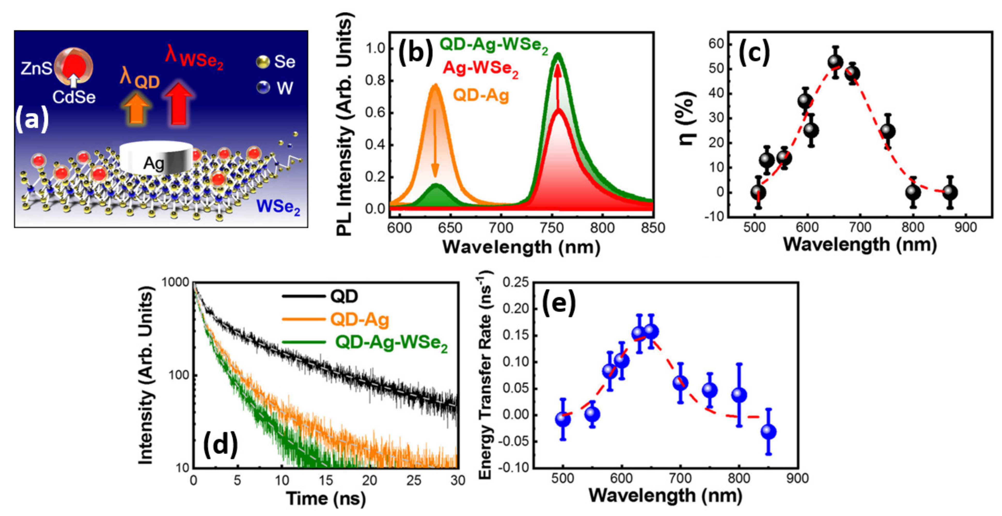
| CdSe/ZnS QD-Ag-WSe2 | The Ag ND was combined with CdSe QDs and monolayer WSe2 to enhance the monolayer WSe2 emission and convert the light from QDs to WSe2 with the highest efficiency of 53%. | [58] |
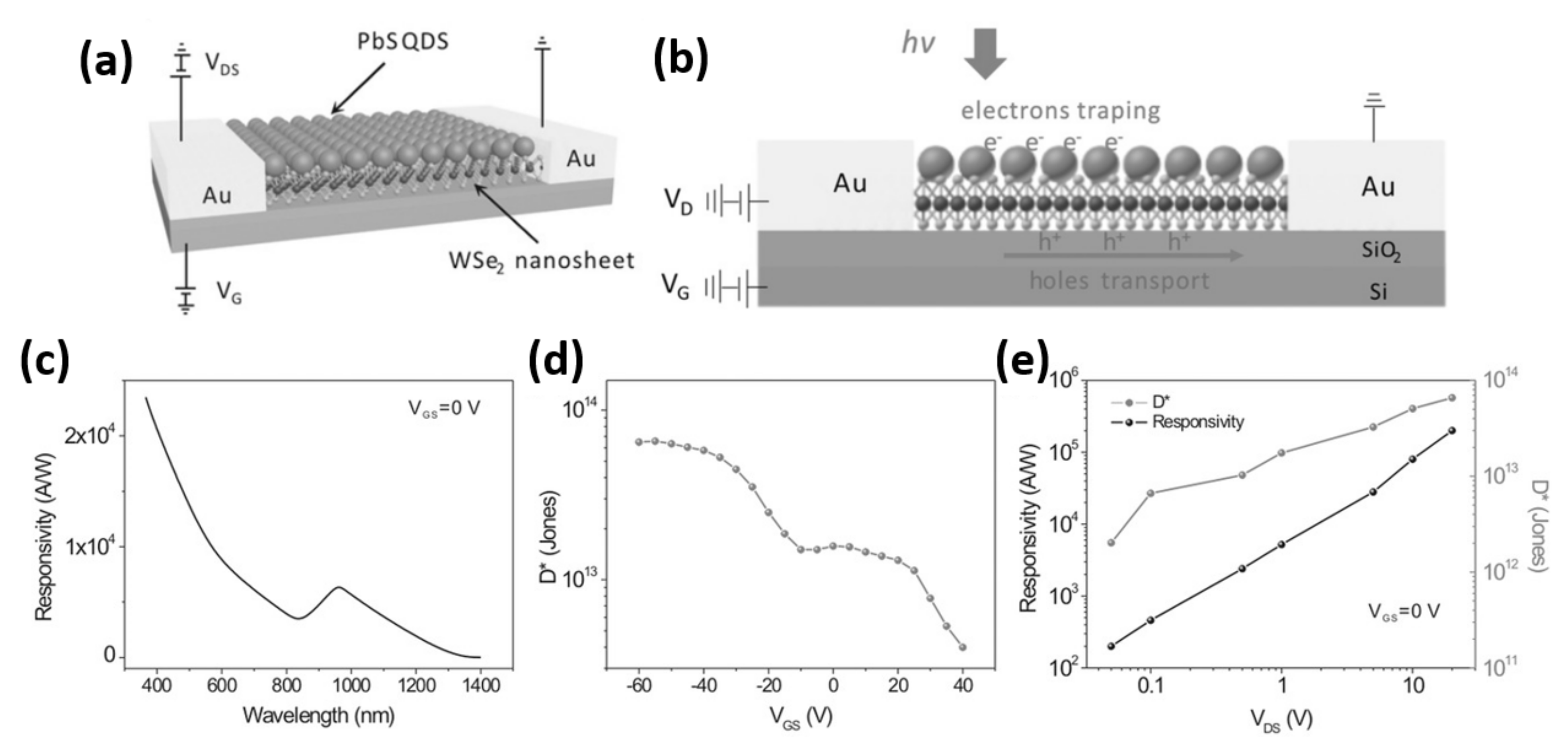
| Hybrid PbS QDs/WSe2 | The hybrid device demonstrated a high responsivity up to 2 × 10⁵ A W–1 and a high specific detectivity of 7 × 10¹³ Jones. | [56] |
| PbS QDs photodiode atop a high-gain graphene phototransistor | The device demonstrated quantum efficiencies in excess of 70%, gain of 105, and 3 dB bandwidth of 1.5 kHz with a measured detectivity of 1 × 10¹³ Jones. | [145] |
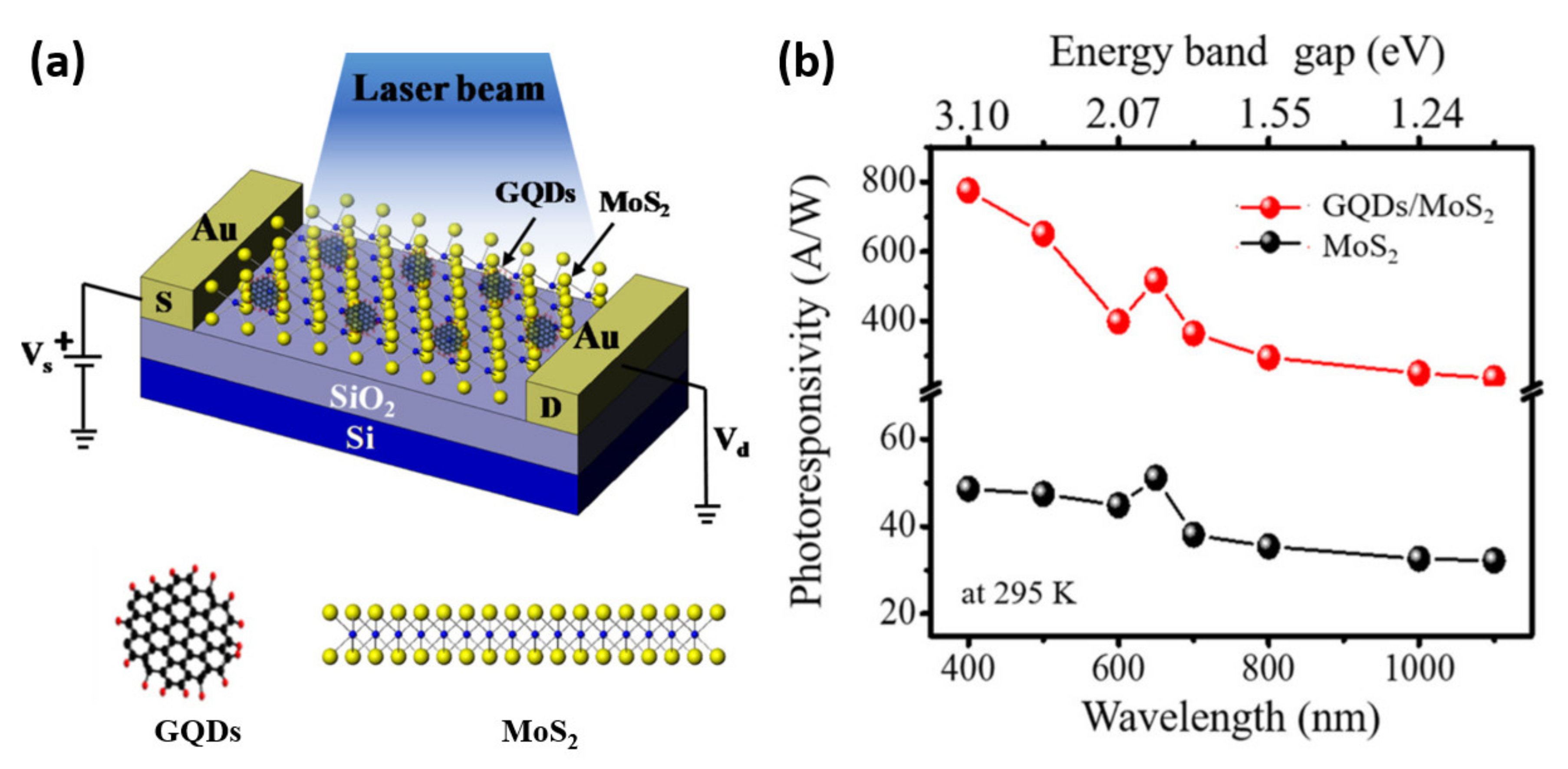
| GQD/MoS2 hybrid photodetector | The device exhibits a photoresponsivity 775 AW–1 at a laser wavelength of 400 nm, a detectivity of 2.33 × 10¹² Jones, and an EQE of about 241%. | [146] |
| WS2 QDs for spintronics and valleytronics | Ultrasmall and monolayered tungsten dichalcogenide QDs with giant spin–valley coupling and purple luminescence for various applications in spintronics and valleytronics. | [154] |
Publisher’s Note: MDPI stays neutral with regard to jurisdictional claims in published maps and institutional affiliations. |
© 2021 by the authors. Licensee MDPI, Basel, Switzerland. This article is an open access article distributed under the terms and conditions of the Creative Commons Attribution (CC BY) license (https://creativecommons.org/licenses/by/4.0/).
Share and Cite
James Singh, K.; Ahmed, T.; Gautam, P.; Sadhu, A.S.; Lien, D.-H.; Chen, S.-C.; Chueh, Y.-L.; Kuo, H.-C. Recent Advances in Two-Dimensional Quantum Dots and Their Applications. Nanomaterials 2021, 11, 1549. https://doi.org/10.3390/nano11061549
James Singh K, Ahmed T, Gautam P, Sadhu AS, Lien D-H, Chen S-C, Chueh Y-L, Kuo H-C. Recent Advances in Two-Dimensional Quantum Dots and Their Applications. Nanomaterials. 2021; 11(6):1549. https://doi.org/10.3390/nano11061549
Chicago/Turabian StyleJames Singh, Konthoujam, Tanveer Ahmed, Prakalp Gautam, Annada Sankar Sadhu, Der-Hsien Lien, Shih-Chen Chen, Yu-Lun Chueh, and Hao-Chung Kuo. 2021. "Recent Advances in Two-Dimensional Quantum Dots and Their Applications" Nanomaterials 11, no. 6: 1549. https://doi.org/10.3390/nano11061549
APA StyleJames Singh, K., Ahmed, T., Gautam, P., Sadhu, A. S., Lien, D.-H., Chen, S.-C., Chueh, Y.-L., & Kuo, H.-C. (2021). Recent Advances in Two-Dimensional Quantum Dots and Their Applications. Nanomaterials, 11(6), 1549. https://doi.org/10.3390/nano11061549