
All-Dielectric Metasurface-Based Beam Splitter with Arbitrary Splitting Ratio

Abstract
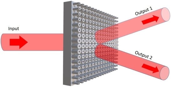
1. Introduction
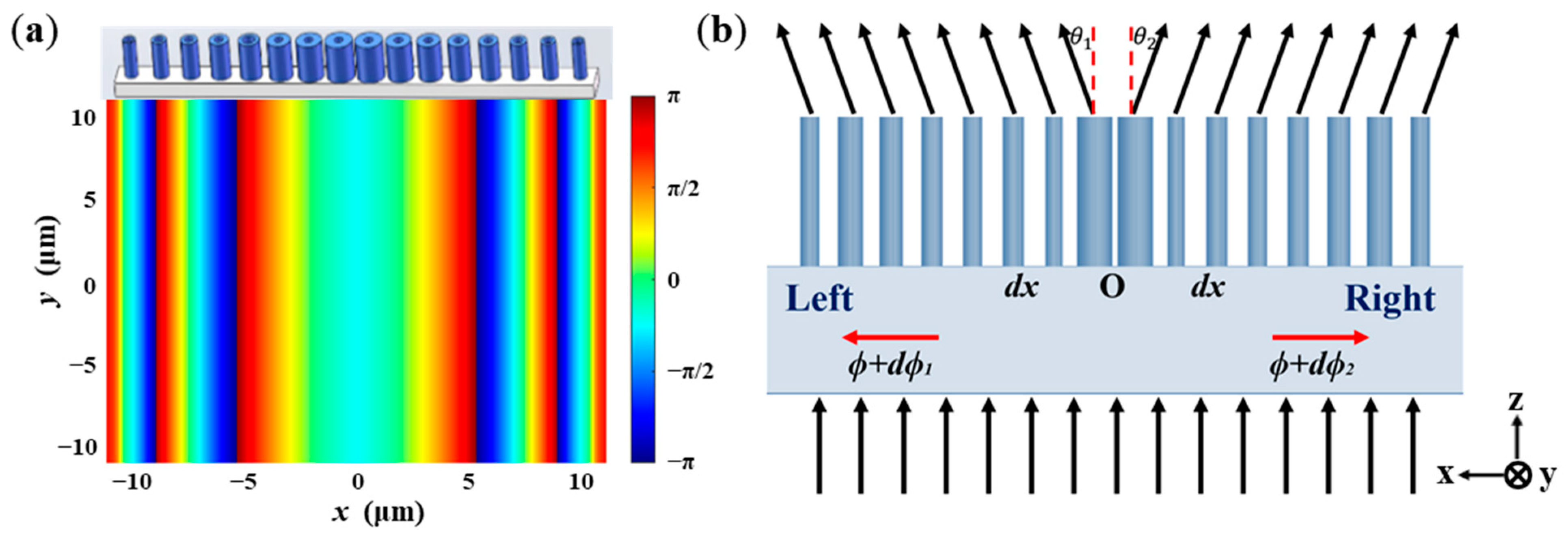
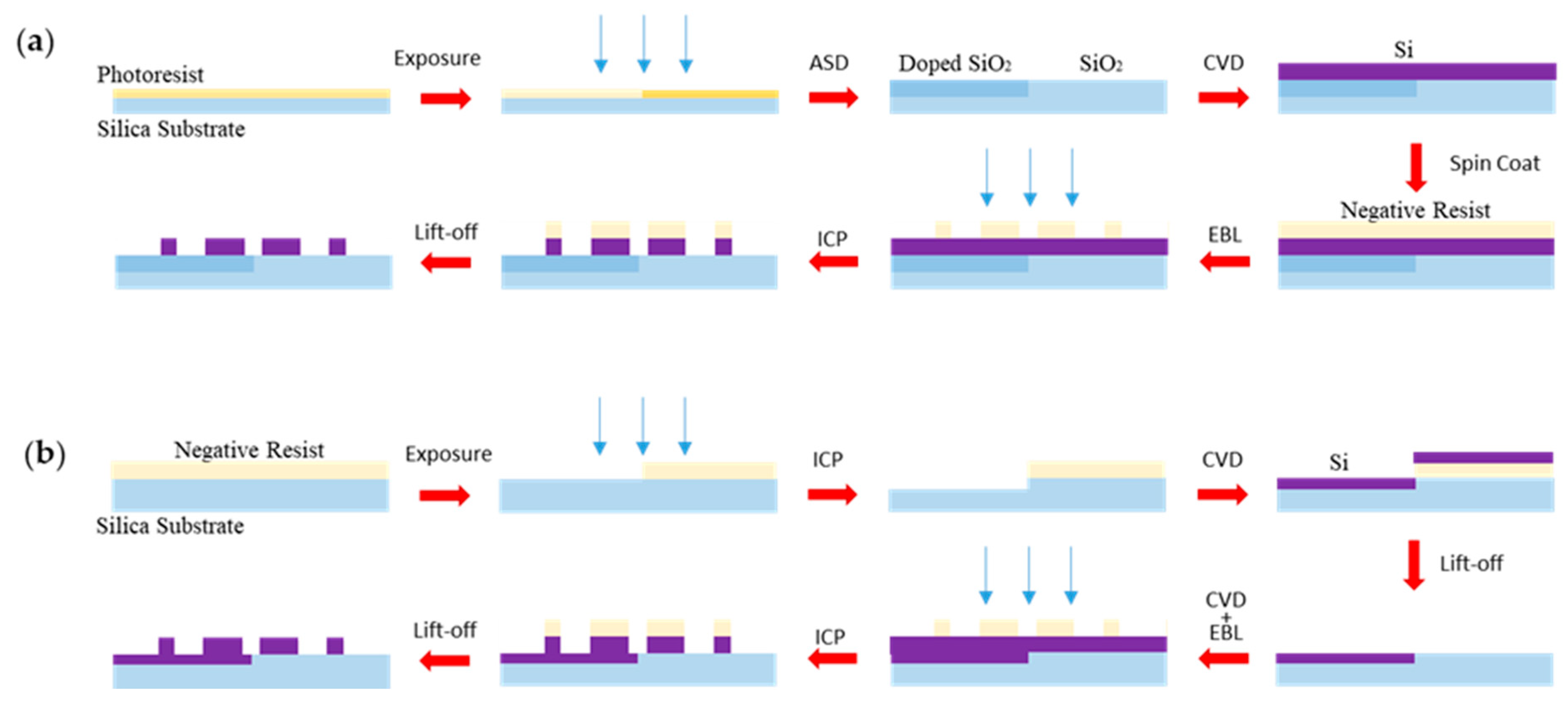
2. Design Methodologies
3. Simulation Results
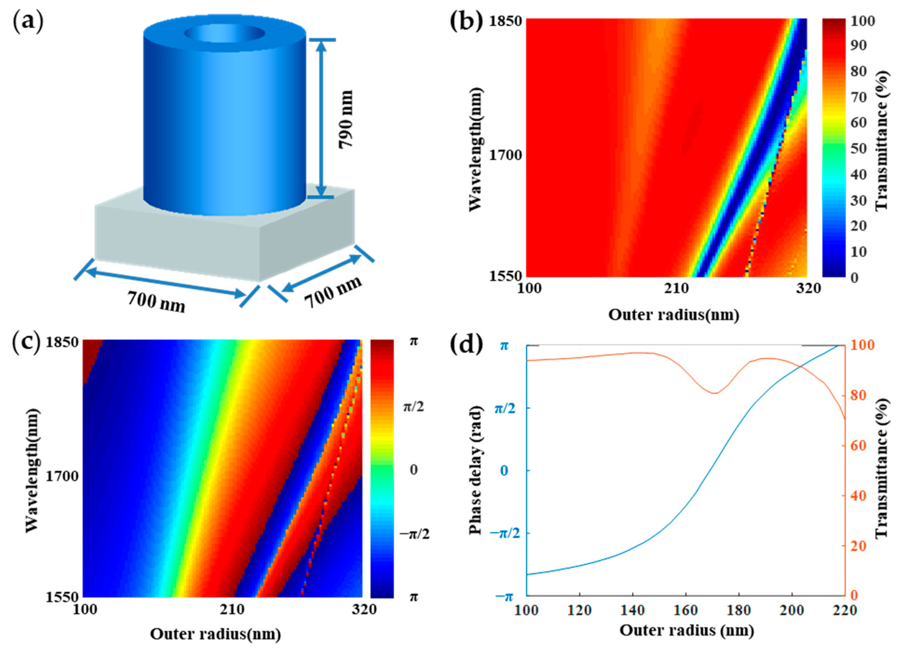
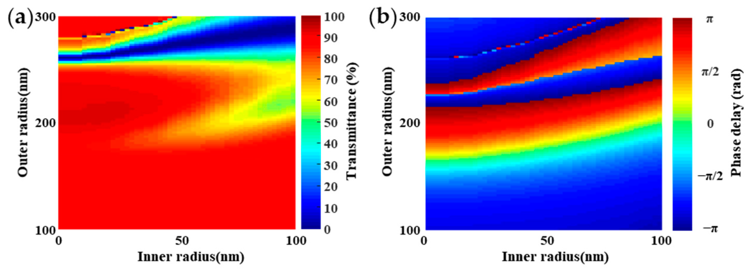
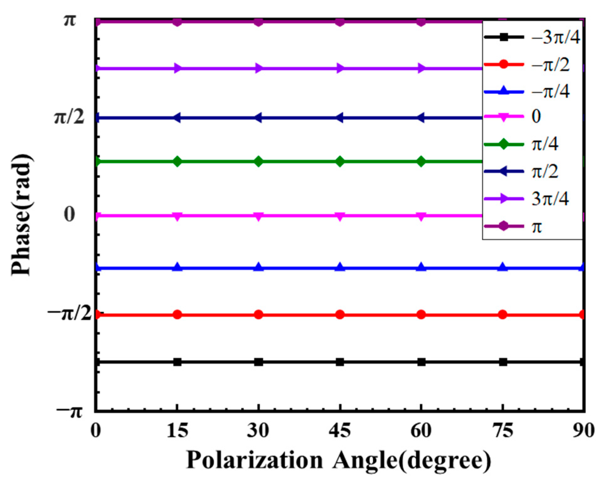
3.1. The Transmittance and Phase Delay of the Structural Elements
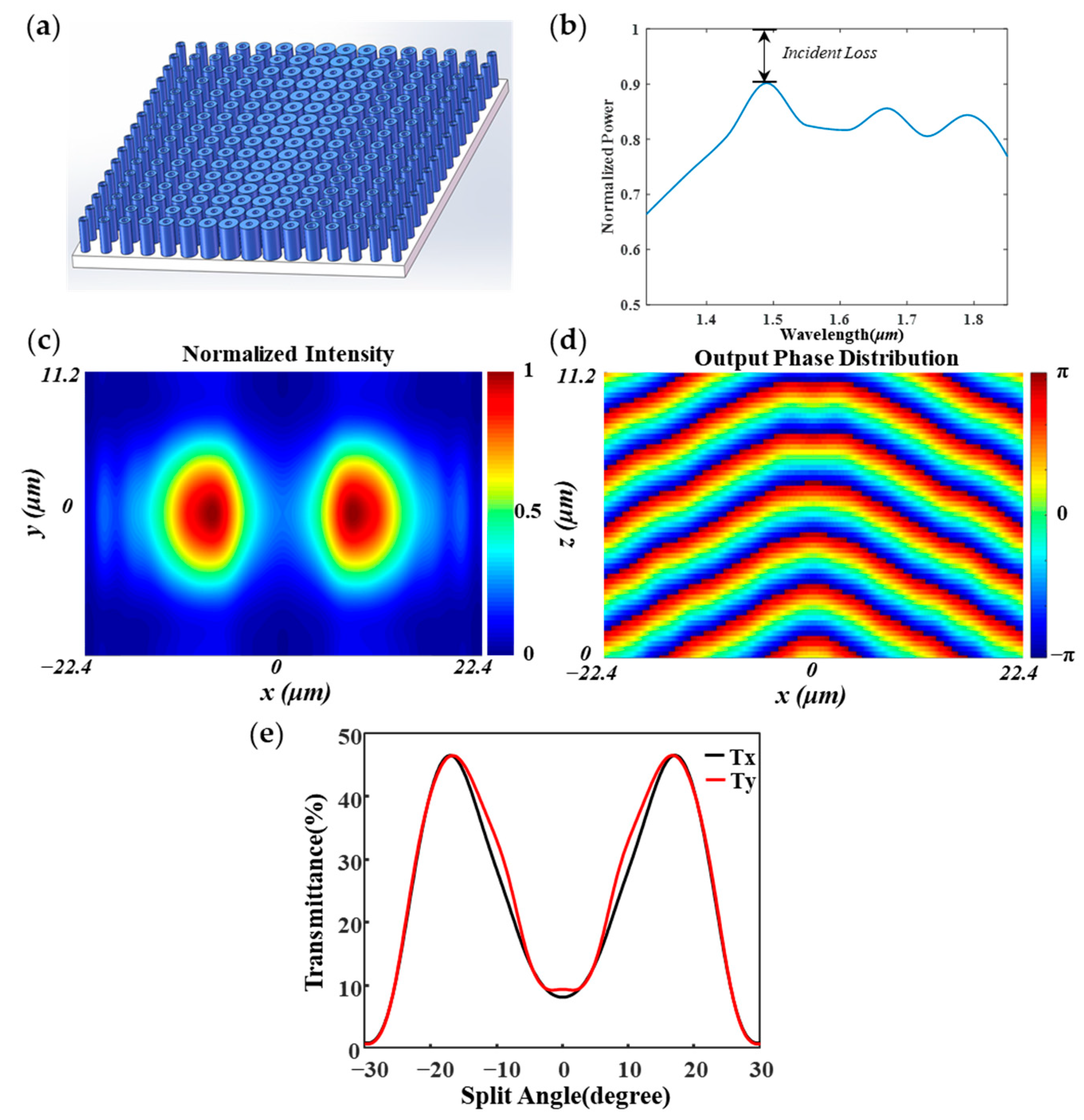
3.2. The Construction of the Beam Splitter
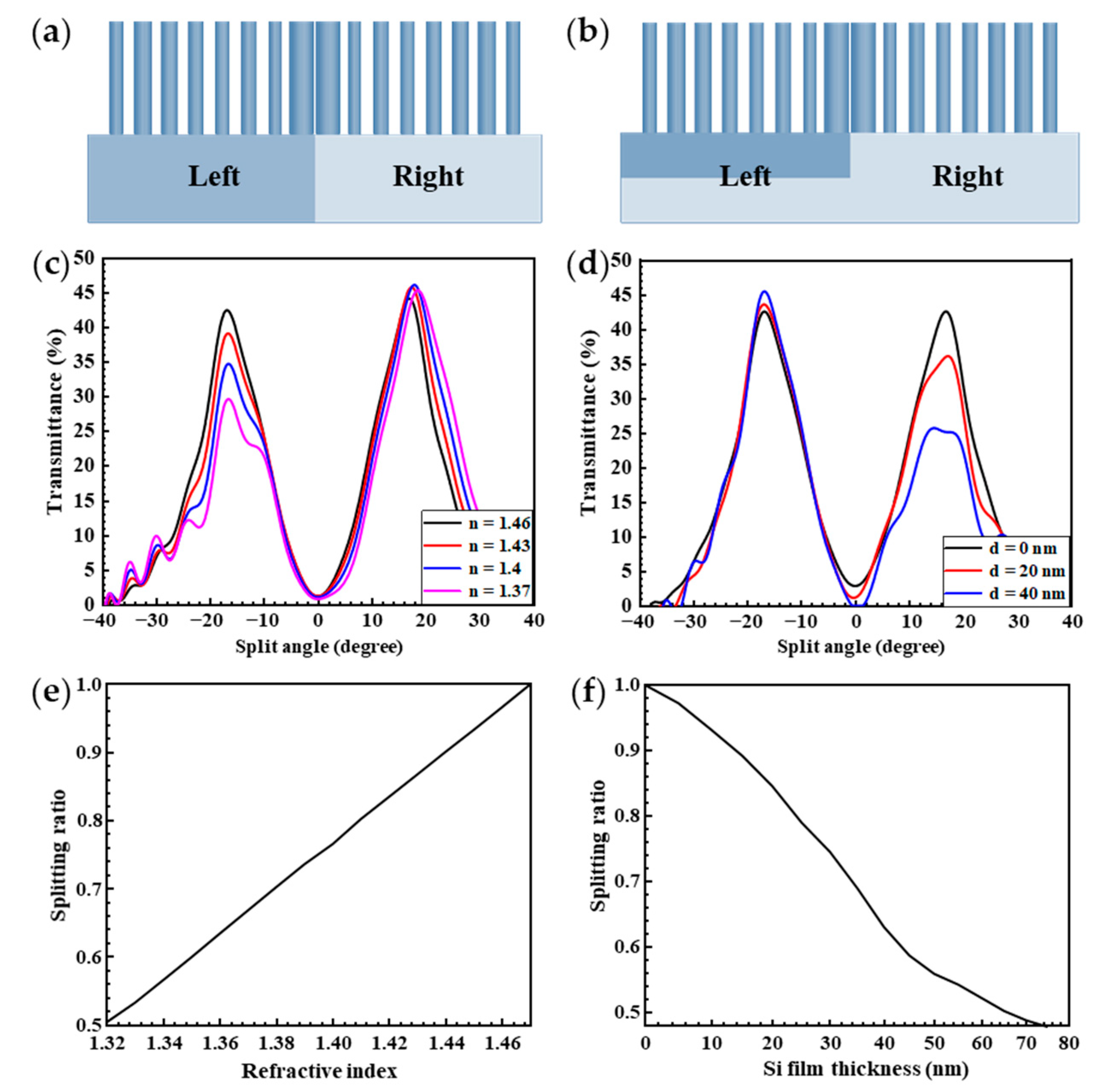
3.3. The Realization of Arbitrary Splitting Ratios
4. Discussion
5. Conclusions
Author Contributions
Funding
Institutional Review Board Statement
Informed Consent Statement
Data Availability Statement
Conflicts of Interest
References
- de Angelis, M.; Tino, G.M. Optical Instruments. In Encyclopedia of Condensed Matter Physics; Bassani, F., Liedl, G.L., Wyder, P., Eds.; Elsevier: Oxford, UK, 2005; pp. 159–175. [Google Scholar]
- Malka, D.; Danan, Y.; Ramon, Y.; Zalevsky, Z. A Photonic 1 × 4 Power Splitter Based on Multimode Interference in Silicon-Gallium-Nitride Slot Waveguide Structures. Materials 2016, 9, 516. [Google Scholar] [CrossRef]
- Samoi, E.; Benezra, Y.; Malka, D. An ultracompact 3 × 1 MMI power-combiner based on Si slot-waveguide structures. Photonics Nanostruct. Fundam. Appl. 2020, 39, 7. [Google Scholar] [CrossRef]
- Moshaev, V.; Leibin, Y.; Malka, D. Optimizations of Si PIN diode phase-shifter for controlling MZM quadrature bias point using SOI rib waveguide technology. Opt. Laser Technol. 2021, 138, 9. [Google Scholar] [CrossRef]
- Rizea, A. Design technique for all-dielectric non-polarizing beam splitter plate. Opto Electron. Rev. 2012, 20, 96–99. [Google Scholar] [CrossRef]
- Feng, J.; Zhou, Z. Polarization beam splitter using a binary blazed grating coupler. Opt. Lett. 2007, 32, 1662–1664. [Google Scholar] [CrossRef] [PubMed]
- Kumar, V.S.P.; Sunita, P.; Kumar, M.; Kumari, N.; Karar, V.; Sharma, A.L. Design and fabrication of multilayer dichroic beam splitter. Adv. Mater. Proc. 2017, 2, 398. [Google Scholar] [CrossRef][Green Version]
- Lin, D.; Fan, P.; Hasman, E.; Brongersma, M.L. Dielectric gradient metasurface optical elements. Science 2014, 345, 298–302. [Google Scholar] [CrossRef] [PubMed]
- Yu, N.; Capasso, F. Flat optics with designer metasurfaces. Nat. Mater. 2014, 13, 139–150. [Google Scholar] [CrossRef]
- Zhao, Y.; Liu, X.-X.; Alù, A. Recent advances on optical metasurfaces. J. Opt. 2014, 16, 123001–123014. [Google Scholar] [CrossRef]
- Chen, S.; Zhou, X.; Luo, Y.; Guo, Q.; Ye, H. Two-Dimensional Material and Metasurface Based Optoelectronics. Adv. Condens. Matter Phys. 2019, 2019, 8365870. [Google Scholar] [CrossRef]
- Wei, Q.; Huang, L.; Zentgraf, T.; Wang, Y. Optical wavefront shaping based on functional metasurfaces. Nanophotonics 2020, 9, 987–1002. [Google Scholar] [CrossRef]
- Yang, B.; He, Y.; Xie, Z.; Liu, J.; Ye, H.; Xiao, J.; Li, Y.; Fan, D.; Chen, S. Dielectric metasurface based polarization and orbital angular momentum demultiplexer. Results Phys. 2021, 20, 103706. [Google Scholar] [CrossRef]
- Huang, L.; Song, X.; Reineke, B.; Li, T.; Li, X.; Liu, J.; Zhang, S.; Wang, Y.; Zentgraf, T. Volumetric generation of optical vortices with metasurfaces. Acs Photonics 2017, 4, 338–346. [Google Scholar] [CrossRef]
- He, Y.; Xie, Z.; Yang, B.; Chen, X.; Liu, J.; Ye, H.; Zhou, X.; Li, Y.; Chen, S.; Fan, D. Controllable photonic spin Hall effect with phase function construction. Photonics Res. 2020, 8, 963–971. [Google Scholar] [CrossRef]
- Genevet, P.; Capasso, F. Holographic optical metasurfaces: A review of current progress. Rep. Prog. Phys. 2015, 78, 024401. [Google Scholar] [CrossRef] [PubMed]
- Zhi-Qiang, X.; Yan-Liang, H.; Pei-Pei, W.; Ming-Yang, S.; Xue-Yu, C.; Bo, Y.; Jun-Min, L.; Xin-Xing, Z.; Ying, L.; Shu-Qing, C. Two-dimensional optical edge detection based on Pancharatnam-Berry phase metasurface. Acta Phys. Sin. 2020, 69, 014101. [Google Scholar]
- Lee, G.Y.; Sung, J.; Lee, B. Recent advances in metasurface hologram technologies. ETRI J. 2019, 41, 10–22. [Google Scholar] [CrossRef]
- Teng, S.; Zhang, Q.; Wang, H.; Liu, L.; Lv, H. Conversion between polarization states based on a metasurface. Photonics Res. 2019, 7, 246–250. [Google Scholar] [CrossRef]
- Mueller, J.B.; Rubin, N.A.; Devlin, R.C.; Groever, B.; Capasso, F. Metasurface polarization optics: Independent phase control of arbitrary orthogonal states of polarization. Phys. Rev. Lett. 2017, 118, 113901. [Google Scholar] [CrossRef]
- Zhang, Y.; Yang, L.; Li, X.-K.; Wang, Y.-L.; Huang, C.-P. Dual functionality of a single-layer metasurface: Polarization rotator and polarizer. J. Opt. 2020, 22, 035101. [Google Scholar] [CrossRef]
- Wang, C.; Yang, B.; Cheng, M.; Cheng, S.; Liu, J.; Xiao, J.; Ye, H.; Li, Y.; Fan, D.; Chen, S. Cylindrical vector beam multiplexing for radio-over-fiber communication with dielectric metasurfaces. Opt. Express 2020, 28, 38666–38681. [Google Scholar] [CrossRef]
- Huang, J.; Li, C.; Lei, Y.; Yang, L.; Xiang, Y.; Curto, A.G.; Li, Z.; Guo, L.; Cao, Z.; Hao, Y. A 20-Gbps Beam-Steered Infrared Wireless Link Enabled by a Passively Field-Programmable Metasurface. Laser Photonics Rev. 2021, 15, 2000266. [Google Scholar] [CrossRef]
- Tang, W.; Chen, M.Z.; Dai, J.Y.; Zeng, Y.; Zhao, X.; Jin, S.; Cheng, Q.; Cui, T.J. Wireless communications with programmable metasurface: New paradigms, opportunities, and challenges on transceiver design. IEEE Wirel. Commun. 2020, 27, 180–187. [Google Scholar] [CrossRef]
- Chen, H.; Xiong, L.; Hu, F.; Xiang, Y.; Dai, X.; Li, G. Ultrasensitive and Tunable Sensor Based on Plasmon-Induced Transparency in a Black Phosphorus Metasurface. Plasmonics 2021, 1–7. [Google Scholar] [CrossRef]
- Gorodkiewicz, E.; Lukaszewski, Z. Recent progress in surface plasmon resonance biosensors (2016 to mid-2018). Biosensors 2018, 8, 132. [Google Scholar] [CrossRef]
- Beruete, M.; Jáuregui-López, I. Terahertz sensing based on metasurfaces. Adv. Opt. Mater. 2020, 8, 1900721. [Google Scholar] [CrossRef]
- Chen, H.-T.; Taylor, A.J.; Yu, N. A review of metasurfaces: Physics and applications. Rep. Prog. Phys. 2016, 79, 076401. [Google Scholar] [CrossRef]
- Liu, B.; Song, K.; Xiao, J. Two-dimensional optical metasurfaces: From plasmons to dielectrics. Adv. Condens. Matter Phys. 2019, 2019, 2329168. [Google Scholar] [CrossRef]
- Choudhury, S.M.; Wang, D.; Chaudhuri, K.; DeVault, C.; Kildishev, A.V.; Boltasseva, A.; Shalaev, V.M. Material platforms for optical metasurfaces. Nanophotonics 2018, 7, 959–987. [Google Scholar] [CrossRef]
- Khorasaninejad, M.; Capasso, F. Metalenses: Versatile multifunctional photonic components. Science 2017, 358, eaam8100. [Google Scholar] [CrossRef] [PubMed]
- Ginn, J.C.; Brener, I.; Peters, D.W.; Wendt, J.R.; Stevens, J.O.; Hines, P.F.; Basilio, L.I.; Warne, L.K.; Ihlefeld, J.F.; Clem, P.G. Realizing Optical Magnetism from Dielectric Metamaterials. Phys. Rev. Lett. 2012, 108, 097402. [Google Scholar] [CrossRef]
- He, Q.; Sun, S.; Xiao, S.; Zhou, L. High-efficiency metasurfaces: Principles, realizations, and applications. Adv. Opt. Mater. 2018, 6, 1800415. [Google Scholar] [CrossRef]
- Kamali, S.M.; Arbabi, E.; Arbabi, A.; Faraon, A. A review of dielectric optical metasurfaces for wavefront control. Nanophotonics 2018, 7, 1041–1068. [Google Scholar] [CrossRef]
- Khorasaninejad, M.; Zhu, W.; Crozier, K.B. Efficient polarization beam splitter pixels based on a dielectric metasurface. Optica 2015, 2, 376–382. [Google Scholar] [CrossRef]
- Khorasaninejad, M.; Crozier, K.B. Silicon nanofin grating as a miniature chirality-distinguishing beam-splitter. Nat. Commun. 2014, 5, 5386. [Google Scholar] [CrossRef] [PubMed]
- Hasani, H.; Tamagnone, M.; Capdevila, S.; Moldovan, C.F.; Maoddi, P.; Ionescu, A.M.; Peixeiro, C.; Mosig, J.R.; Skrivervik, A.K.; Perruisseau-Carrier, J. Tri-band, polarization-independent reflectarray at terahertz frequencies: Design, fabrication, and measurement. IEEE Trans. Terahertz Sci. Technol. 2016, 6, 268–277. [Google Scholar] [CrossRef]
- Li, Z.; Palacios, E.; Butun, S.; Aydin, K. Visible-frequency metasurfaces for broadband anomalous reflection and high-efficiency spectrum splitting. Nano Lett. 2015, 15, 1615–1621. [Google Scholar] [CrossRef]
- Yu, N.; Genevet, P.; Kats, M.A.; Aieta, F. Light propagation with phase discontinuities: Generalized laws of reflection and refraction. Science 2011, 334, 333–337. [Google Scholar] [CrossRef] [PubMed]
- Zhang, X.; Tian, Z.; Yue, W.; Gu, J.; Zhang, S.; Han, J.; Zhang, W. Broadband terahertz wave deflection based on C-shape complex metamaterials with phase discontinuities. Adv. Mater. 2013, 25, 4567–4572. [Google Scholar] [CrossRef]
- Wei, M.; Xu, Q.; Wang, Q.; Zhang, X.; Li, Y.; Gu, J.; Tian, Z.; Zhang, X.; Han, J.; Zhang, W. Broadband non-polarizing terahertz beam splitters with variable split ratio. Appl. Phys. Lett. 2017, 111, 071101. [Google Scholar] [CrossRef]
- Khorasaninejad, M.; Chen, W.T.; Devlin, R.C.; Oh, J.; Zhu, A.Y.; Capasso, F. Metalenses at visible wavelengths: Diffraction-limited focusing and subwavelength resolution imaging. Science 2016, 352, 1190–1194. [Google Scholar] [CrossRef] [PubMed]
- Arbabi, A.; Horie, Y.; Bagheri, M.; Faraon, A. Dielectric metasurfaces for complete control of phase and polarization with subwavelength spatial resolution and high transmission. Nat. Nanotechnol. 2015, 10, 937–943. [Google Scholar] [CrossRef]
- Joyce, B.; Baldrey, J. Selective epitaxial deposition of silicon. Nature 1962, 195, 485–486. [Google Scholar] [CrossRef]
- Parsons, G.N.; Clark, R.D. Area-Selective Deposition: Fundamentals, Applications, and Future Outlook. Chem. Mater. 2020, 32, 4920–4953. [Google Scholar] [CrossRef]


| Rout (nm) | 216 | 144 | 150 | 160 | 168 | 172 | 180 | 196 | 214 |
| Rin (nm) | 22 | 94 | 48 | 26 | 28 | 12 | 12 | 28 | 8 |
| Phase | −π | −3π/4 | −π/2 | −π/4 | 0 | π/4 | π/2 | 3π/4 | π |
| T (%) | 99.88 | 96.83 | 96.69 | 96.112 | 93.56 | 93.20 | 92.82 | 96.35 | 99.48 |
Publisher’s Note: MDPI stays neutral with regard to jurisdictional claims in published maps and institutional affiliations. |
© 2021 by the authors. Licensee MDPI, Basel, Switzerland. This article is an open access article distributed under the terms and conditions of the Creative Commons Attribution (CC BY) license (https://creativecommons.org/licenses/by/4.0/).
Share and Cite
Chen, X.; Zou, H.; Su, M.; Tang, L.; Wang, C.; Chen, S.; Su, C.; Li, Y. All-Dielectric Metasurface-Based Beam Splitter with Arbitrary Splitting Ratio. Nanomaterials 2021, 11, 1137. https://doi.org/10.3390/nano11051137
Chen X, Zou H, Su M, Tang L, Wang C, Chen S, Su C, Li Y. All-Dielectric Metasurface-Based Beam Splitter with Arbitrary Splitting Ratio. Nanomaterials. 2021; 11(5):1137. https://doi.org/10.3390/nano11051137
Chicago/Turabian StyleChen, Xueyu, Haijian Zou, Mingyang Su, Linwei Tang, Chaofeng Wang, Shuqing Chen, Chenliang Su, and Ying Li. 2021. "All-Dielectric Metasurface-Based Beam Splitter with Arbitrary Splitting Ratio" Nanomaterials 11, no. 5: 1137. https://doi.org/10.3390/nano11051137
APA StyleChen, X., Zou, H., Su, M., Tang, L., Wang, C., Chen, S., Su, C., & Li, Y. (2021). All-Dielectric Metasurface-Based Beam Splitter with Arbitrary Splitting Ratio. Nanomaterials, 11(5), 1137. https://doi.org/10.3390/nano11051137