
Blue Electroluminescence in SRO-HFCVD Films

 ,
,  , , , , , ,
Abstract
1. Introduction
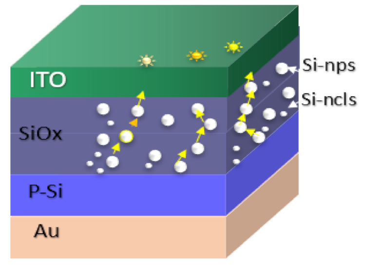
2. Materials and Methods
3. Results and Discussion
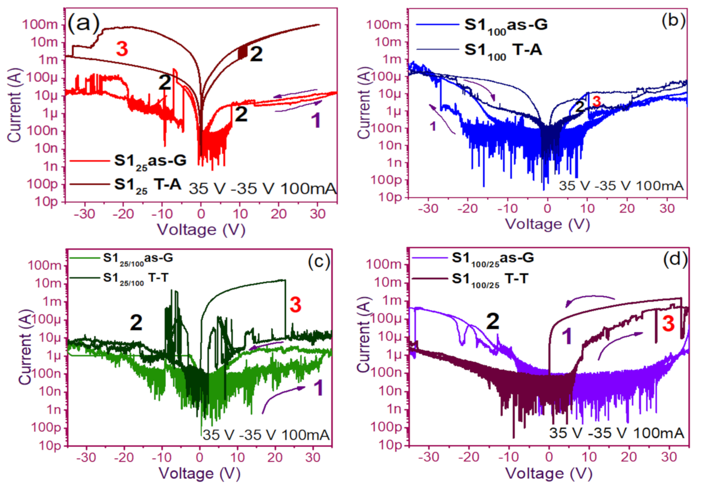
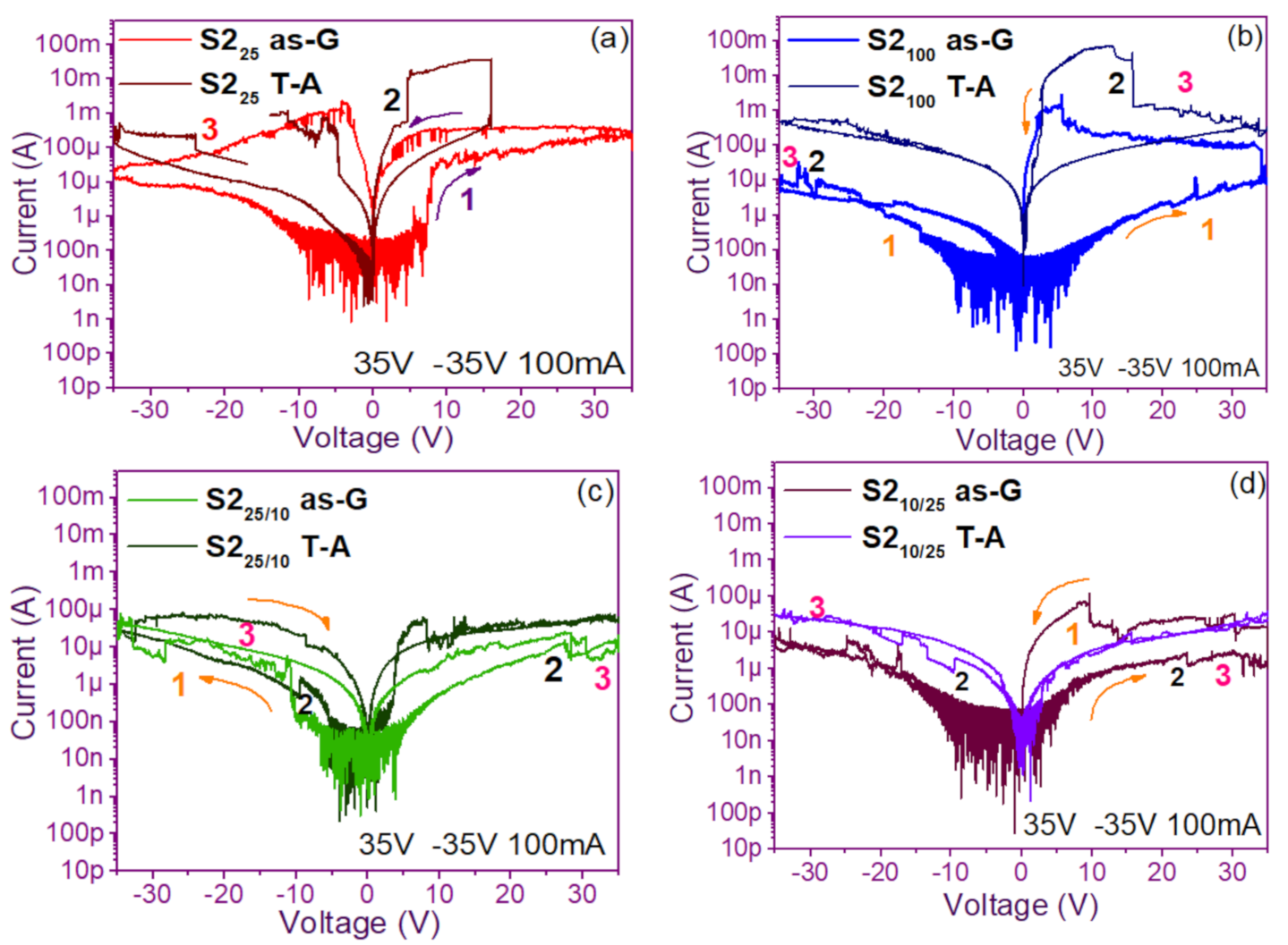
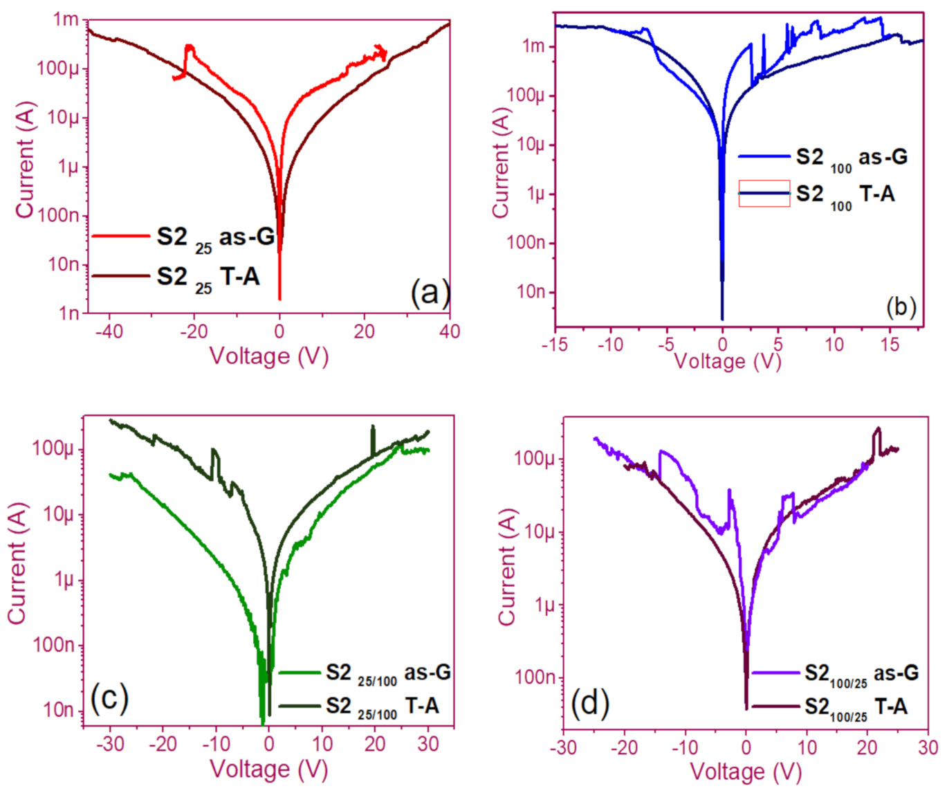
3.1. Curves I-V Pristine of Structures
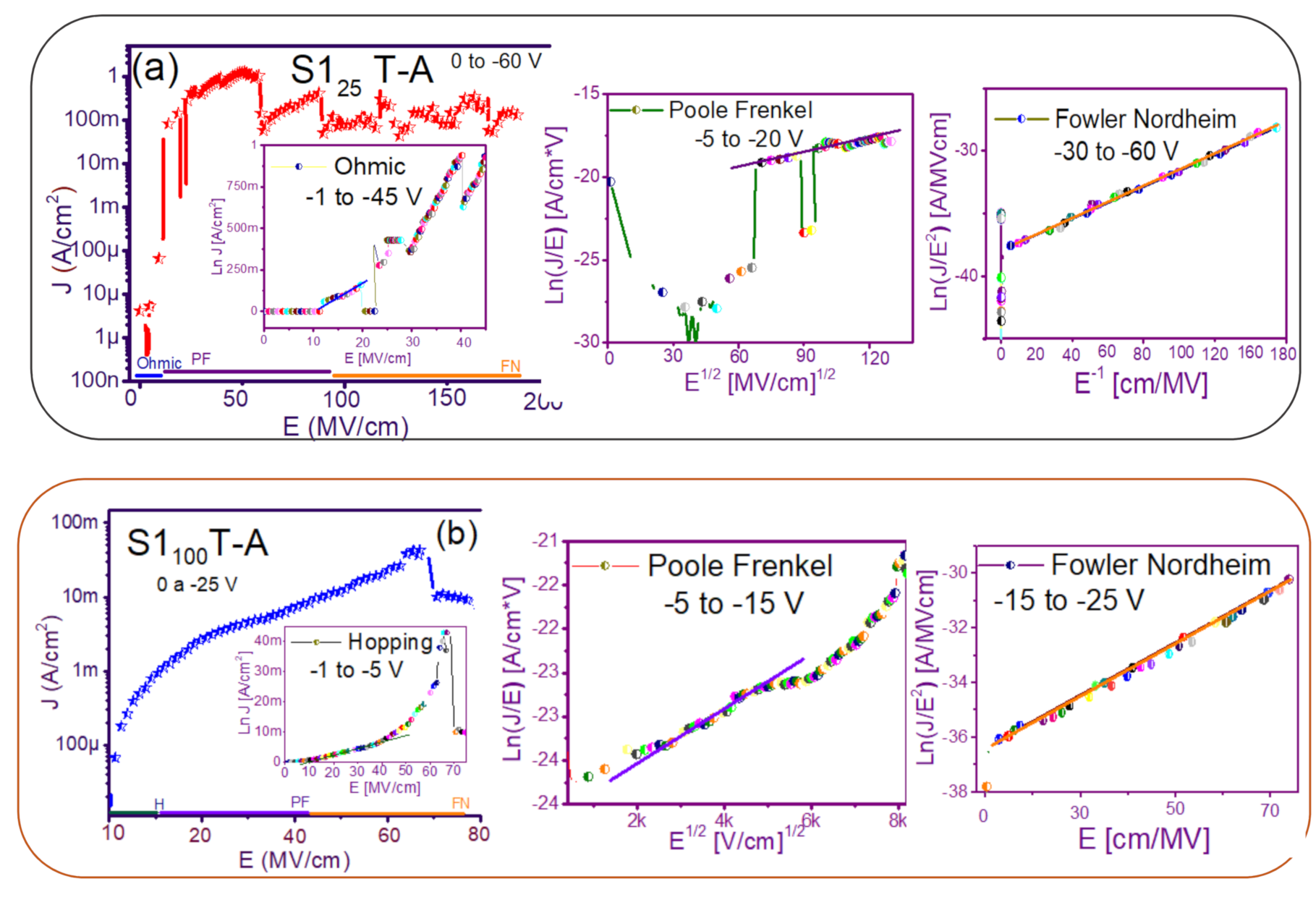
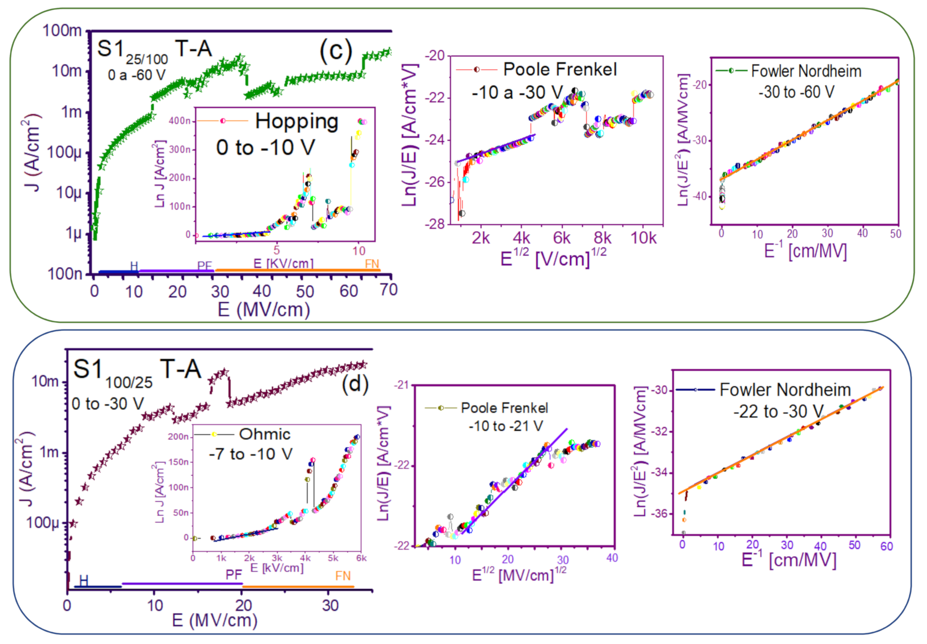
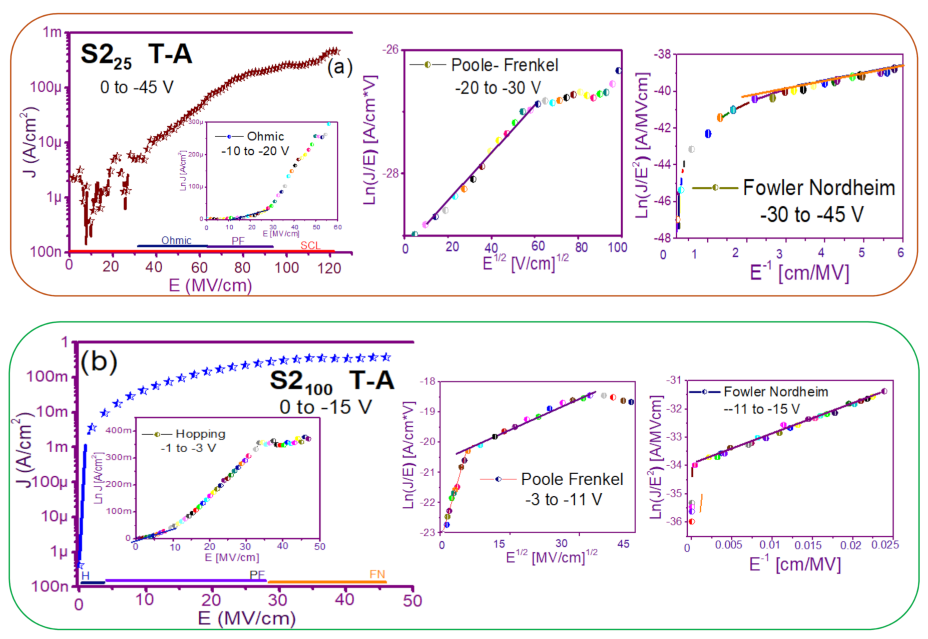
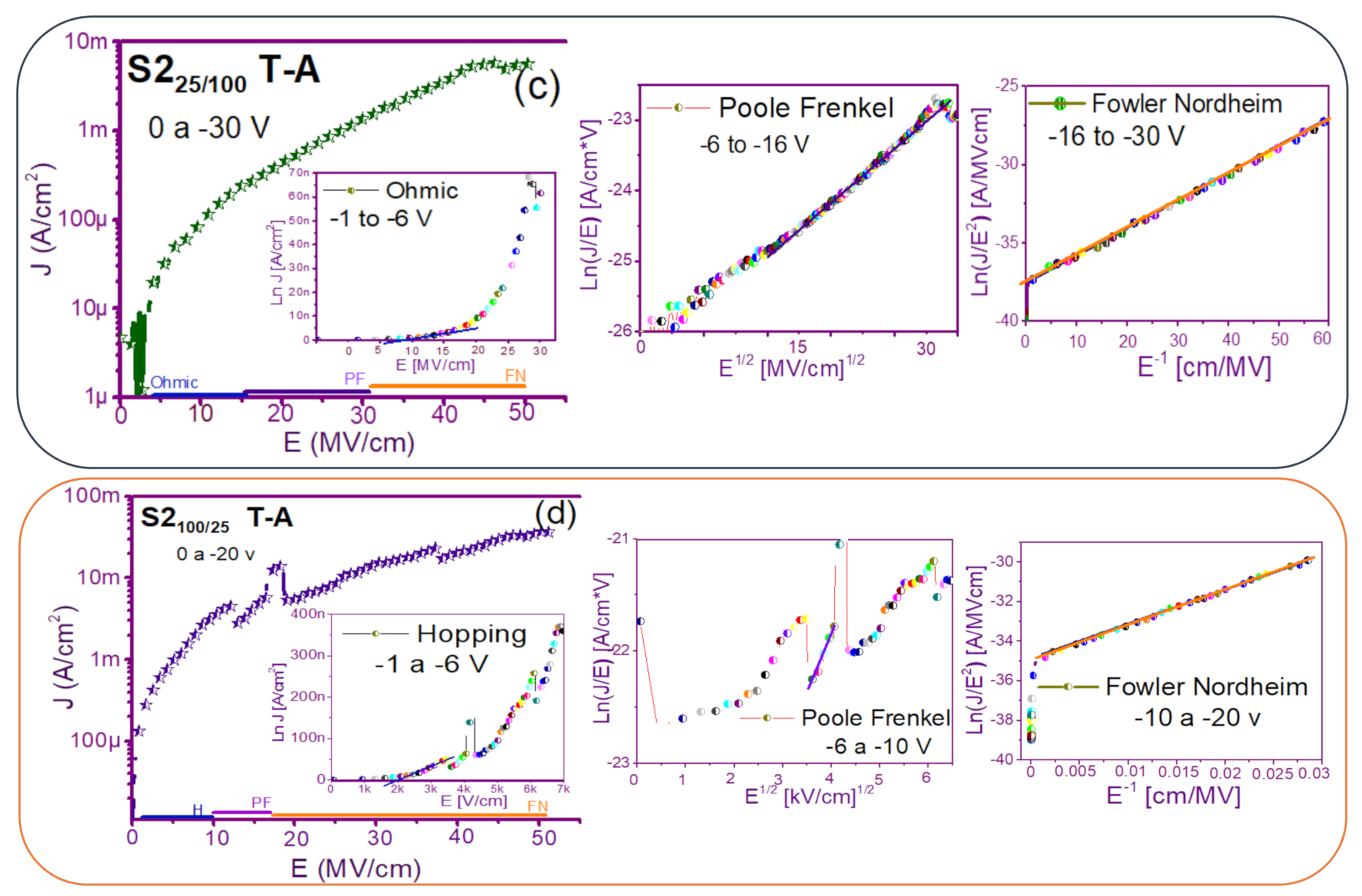
3.2. Conduction Mechanisms
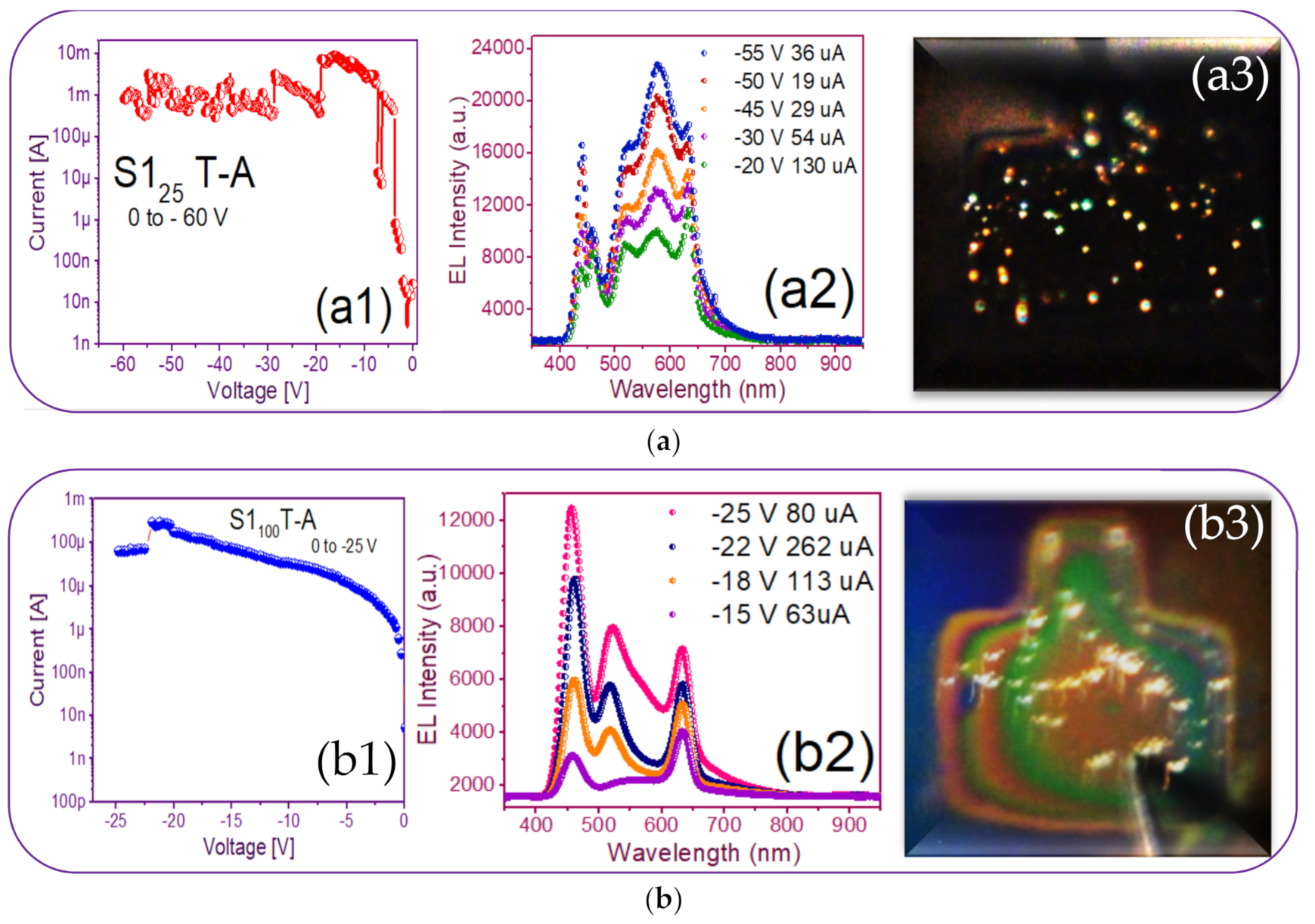
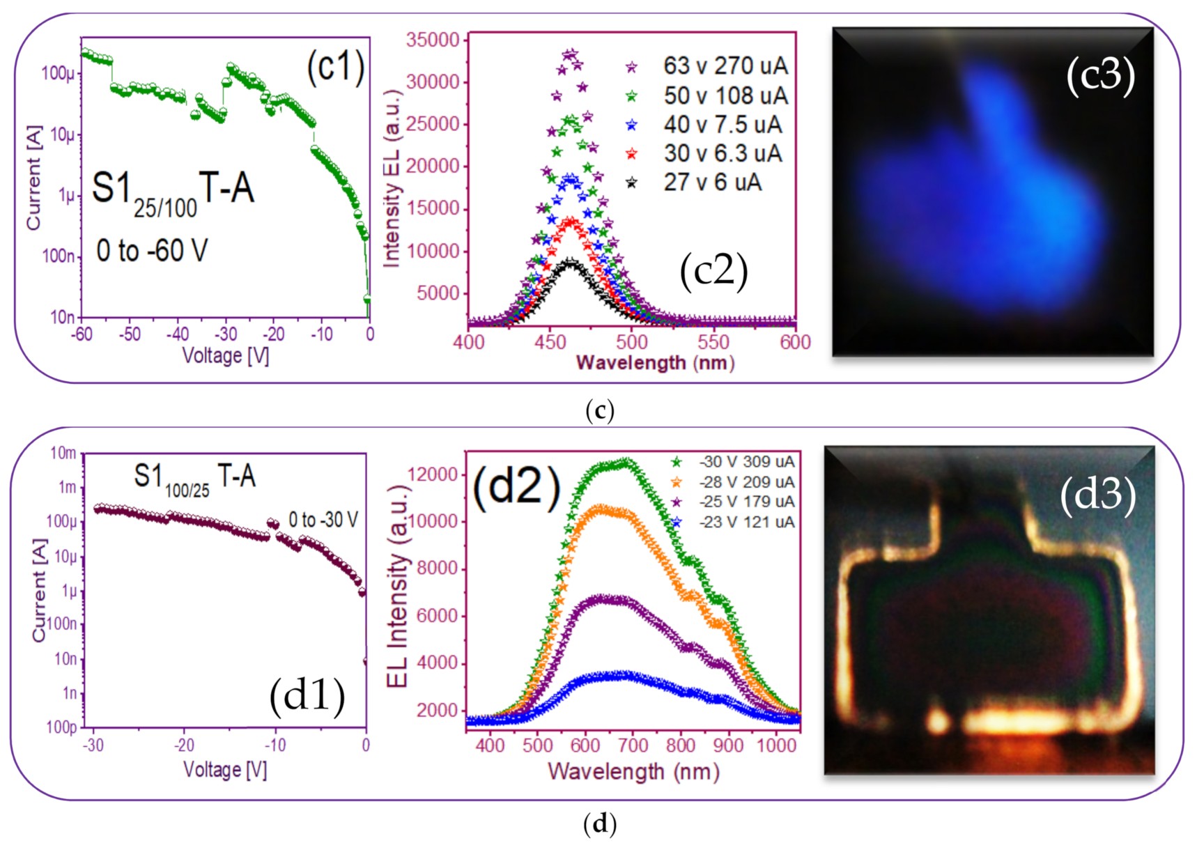
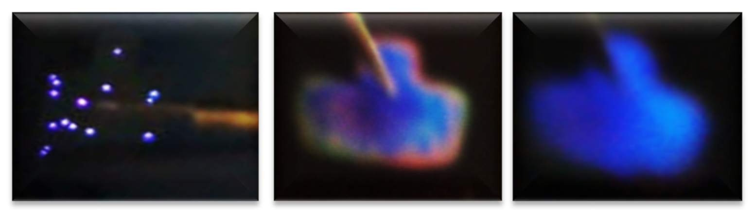
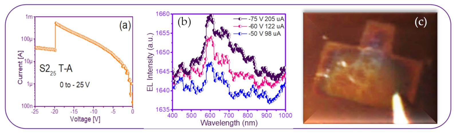
3.3. Electroluminescent Structures
4. Conclusions
Author Contributions
Funding
Institutional Review Board Statement
Informed Consent Statement
Acknowledgments
Conflicts of Interest
References
- Shi, Z.; Lei, L.; Li, Y.; Zhang, F.; Ma, Z.; Li, X.; Wu, D.; Xu, T.; Tian, Y.; Zhang, B.; et al. Hole-Injection Layer-Free Perovskite Light-Emitting Diodes. ACS Appl. Mater. Interfaces 2018, 10, 32289–32297. [Google Scholar] [CrossRef] [PubMed]
- Shi, Z.; Li, Y.; Zhang, Y.; Wu, D.; Xu, T.; Zhang, B.; Liang, L.; Li, X.; Du, G. Electrically Pumped Ultraviolet Lasing in Polygonal Hollow Microresonators: Investigation on Optical Cavity Effect. Opt. Lett. 2016, 41, 5608–5611. [Google Scholar] [CrossRef] [PubMed]
- Dussan, A.; Garzón, A.D.; Malambo Martinez, J.E. Optical Properties of Polycrystalline Silicon Thin Films Deposited Varying Power Range By PECVD Method. Rev. Colomb. Fís. 2011, 43, 377. [Google Scholar]
- Ceiler, M.F.; Kohl, P.A.; Bidstrup, S.A. Plasma-Enhanced Chemical Vapor Deposition of Silicon Dioxide Deposited at Low Temperatures. J. Electrochem. Soc. 1995, 142, 2067–2071. [Google Scholar] [CrossRef]
- Roschuk, T.; Wojcik, J.; Tan, X.; Davies, J.A.; Mascher, P. Optical and Compositional Characterization of SiOxNy and SiOx Thin Films Deposited by Electron Cyclotron Resonance Plasma-Enhanced Chemical Vapor Deposition. J. Vac. Sci. Technol. A Vac. Surf. Films 2004, 22, 883–886. [Google Scholar] [CrossRef]
- Pankove, J. Optical Process in Semiconductors; Prentice-Hall: Englewood, IL, USA, 1971. [Google Scholar]
- Choi, K.C.; Saville, G.F.; Lee, S.C. Microbridge Plasma Display Panel with High Gas Pressure. IEEE Trans. Electron. Devices 1998, 45, 1356–1360. [Google Scholar] [CrossRef]
- Lane, S.N.; Westaway, R.M.; Hicks, D.M. Estimation of Erosion and Deposition Volumes in a Large, Gravel-Bed, Braided River Using Synoptic Remote Sensing. Earth Surf. Processes Landforms 2003, 28, 249–271. [Google Scholar] [CrossRef]
- Aceves, M.; Carrillo, J.; Carranza, J.; Calleja, W.; Falcony, C.; Rosales, P. Duality Metal Oxide Semiconductor P-N Junction in the Al/Silicon Rich Oxide/Si Structure as a Radiation Sensor. Thin Solid Films 2000, 373, 134–136. [Google Scholar] [CrossRef]
- Luna-López, J.; García-Salgado, G.; Díaz-Becerril, T.; López, J.C.; Vázquez-Valerdi, D.; Juárez-Santiesteban, H.; Rosendo-Andrés, E.; Coyopol, A. FTIR, AFM and PL Properties of Thin SiOx Films Deposited by HFCVD. Mater. Sci. Eng. B 2010, 174, 88–92. [Google Scholar] [CrossRef]
- Pai, P.G.; Chao, S.; Takagi, Y.; Lucovsky, G. Infrared Spectroscopic Study of Siox Films Produces By Plasma-Enhanced Chemical Vapor Deposition. J. Vac. Sci. Technol. A 1986, 4, 689–694. [Google Scholar] [CrossRef]
- González-Fernández, A.A.; Mijares, M.A.; Yu, Z.; Sanchez, A.M.; Leyva, K.M. MOS-like Electroluminescent Devices Using Silicon-Rich Oxide Obtained by LPCVD. In Proceedings of the 2009 6th International Conference on Electrical Engineering, Computing Science and Automatic Control (CCE) 2009, Toluca, México, 10–13 January 2009; Volume 2, pp. 611–615. [Google Scholar] [CrossRef]
- Quiroga, E.; Bensch, W.; Yu, Z.; Aceves, M.; De Souza, R.A.; Martin, M.; Zaporojtchenko, V.; Faupel, F. Structural Characteristics of a Multilayer of Silicon Rich Oxide (SRO) with High Si Content Prepared by LPCVD. Phys. Status Solidi 2009, 206, 263–269. [Google Scholar] [CrossRef]
- Aceves-Mijares, M.; González-Fernández, A.A.; López-Estopier, R.; Luna-López, A.; Berman-Mendoza, D.; Morales, A.; Falcony, C.; Domínguez, C.; Murphy-Arteaga, R. On the Origin of Light Emission in Silicon Rich Oxide Obtained by Low-Pressure Chemical Vapor Deposition. J. Nanomater. 2012, 2012, 890701. [Google Scholar] [CrossRef]
- Cui, Y.; Wei, Q.; Park, H.; Lieber, C.M. Nanowire Nanosensors for Highly Sensitive and Selective Detection of Biological and Chemical Species. Science 2001, 293, 1289–1292. [Google Scholar] [CrossRef]
- DiMaria, D.J.; Dong, D.W.; Falcony, C.; Theis, T.N.; Kirtley, J.R.; Tsang, J.C.; Young, D.R.; Pesavento, F.L.; Brorson, S.D. Charge Transport and Trapping Phenomena in Off-Stoichiometric Silicon Dioxide Films. J. Appl. Phys. 1983, 54, 5801–5827. [Google Scholar] [CrossRef]
- Canham, L.T. Silicon Quantum Wire Array Fabrication by Electrochemical and Chemical Dissolution of Wafers. Appl. Phys. Lett. 1990, 57, 1046–1048. [Google Scholar] [CrossRef]
- Zamchiy, A.; Baranov, E.; Merkulova, I.; Khmel, S.; Maximovskiy, E. Determination of the Oxygen Content in Amorphous SiOx Thin Films. J. Non-Cryst. Solids 2019, 518, 43–50. [Google Scholar] [CrossRef]
- Sarikov, A. Crystallization Behavior of Amorphous Si Nanoinclusions Embedded in Silicon Oxide Matrix. Phys. Status solidi 2019, 217, 1900513. [Google Scholar] [CrossRef]
- Klingsporn, M.; Kirner, S.; Villringer, C.; Abou-Ras, D.; Costina, I.; Lehmann, M.; Stannowski, B. Resolving the Nanostructure of Plasma-Enhanced Chemical Vapor Deposited Nanocrystalline SiOx Layers for Application in Solar Cells. J. Appl. Phys. 2016, 119, 223104. [Google Scholar] [CrossRef]
- Smirnov, V.; Lambertz, A.; Moll, S.; Bär, M.; Starr, D.E.; Wilks, R.G.; Finger, F. Doped Microcrystalline Silicon Oxide Alloys for Silicon-Based Photovoltaics: Optoelectronic Properties, Chemical Composition, and Structure Studied by Advanced Characterization Techniques. Phys. Status Solidi 2016, 213, 1814–1820. [Google Scholar] [CrossRef]
- Vázquez Valerdi, D.E.; Luna López, J.A.; García Salgado, G. Twofold SiOx Films Deposited by HFCVD: It is Optical, Compositional and Electrical Properties. Proced. Eng. 2014, 87, 168–171. [Google Scholar] [CrossRef][Green Version]
- Hernandez-Simón, Z.J.; López, J.A.L.; De La Luz, A.D.H.; García, S.A.P.; Lara, A.B.; Salgado, G.G.; López, J.C.; Conde, G.O.M.; Hernández, H.P.M. Spectroscopic Properties of Si-nc in SiOx Films Using HFCVD. Nanomaterials 2020, 10, 1415. [Google Scholar] [CrossRef]
- Flores Gracia, F.; Aceves, M.; Carrillo, J.; Domínguez, C.; Falcony, C. Photoluminescence and Cathodoluminescence Characteristics of SiO2 and SRO Films Implanted with Si. Superf. y Vacío 2005, 18, 7–13. [Google Scholar]
- Fu, S.W.; Chen, H.J.; Wu, H.T.; Shih, C.F. Enhancing Crystallization of Silicon Nanocrystal Embedded in Silicon-Rich Oxide by Ion Beam-Assisted Sputtering. Mater. Sci. Semicond. Process. 2016, 56, 1–4. [Google Scholar] [CrossRef]
- Jaeger, R.C. Introduction to Microelectronic Fabrication; Addison-Wesley Publishing Company: Upper Saddle River, NJ, USA, 1990. [Google Scholar]
- Berencén, Y.; Ramírez, J.M.; Jambois, O.; Domínguez, C.; Rodríguez, J.A.; Garrido, B.J. Correlation between Charge Trasnport and Electroluminescence Properties of Si-Rich Oxide/Nitride/Oxide-Based Light Emitting Capacitors. J. Appl. Phys. 2012, 112, 022114. [Google Scholar]
- Luna-López, J.A.; Carrillo-López, J.; Aceves-Mijares, M.; Morales-Sánchez, Y.A.; Falcony, C. FTIR and photoluminescence of Annealed Silicon Rich Oxide Films. Superf. y Vacío 2009, 22, 11–14. [Google Scholar]
- Benítez-Lara, A.; García-Salgado, G.; Vázquez-Valerdi, D.; Morales-Sánchez, A.; Espinosa-Torres, N.; Luna-López, J. Silicon Rich Oxide Powders by HWCVD: Its Optical and Morphological Properties. Adv. Powder Technol. 2015, 26, 163–168. [Google Scholar] [CrossRef]
- Tai, H.-Y.; Lee, C.-T.; Tsai, L.-H.; Lin, Y.-H.; Pai, Y.-H.; Wu, C.-I.; Lin, G.-R. SiC and Si Quantum Dots Co-Precipitated Si-Rich SiC Film with n- and p-Type Dopants Grown by Hydrogen-Free PECVD. ECS J. Solid State Sci. Technol. 2013, 2, N159–N164. [Google Scholar] [CrossRef]
- Hsieh, C.-R.; Chen, Y.-Y.; Lou, J.-C. Effect of fluorinated silicate glass passivation layer on electrical characteristics and dielectric reliabilities for the HfO2/SiON gate stacked nMOSFET. Microelectron. Eng. 2010, 87, 2241–2246. [Google Scholar] [CrossRef]
- Peralvarez, M.; Barreto, J.; Carreras, J.; Morales, A.; Navarro-Urrios, D.; Lebour, Y.; Dominguez, C.; Garrido, B. Si-nanocrystal-based LEDs fabricated by ion implantation and plasmaenhanced chemical vapour deposition. Nanotechnology 2009, 20, 405201. [Google Scholar] [CrossRef]
- Martínez-Hernández, H.; López, J.L.; Mijares, M.A.; Leyva, K.M.; Salgado, G.G.; Hernández-De-La-Luz, J.; Flores, A.L.; Morales-Caporal, R.; Amador, R.R.; Simón, Z.H. Photoluminescence comparison of SRO-LPCVD films deposited on quartz, polysilicon and silicon substrates. J. Lumin 2019, 216, 116709. [Google Scholar] [CrossRef]
- Chiu, F.-C. A Review on Conduction Mechanisms in Dielectric Films. Adv. Mater. Sci. Eng. 2014, 2014, 578168. [Google Scholar] [CrossRef]
- Ma, H.-P.; Yang, J.-H.; Yang, J.-G.; Zhu, L.-Y.; Huang, W.; Yuan, G.-J.; Feng, J.-J.; Jen, T.-C.; Lu, H.-L. Systematic Study of the SiOx Film with Different Stoichiometry by Plasma-Enhanced Atomic Layer Deposition and Its Application in SiOx/SiO2 Super-Lattice. Nanomaterials 2019, 9, 55. [Google Scholar] [CrossRef] [PubMed]
- Dimaria, D.J.; Ghez, R.; Dong, D.W. Charge Trapping Studies in SiO2 Using High Current Injection from Si-Rich SiO2. J. Appl. Phys. 1980, 51, 4830–4841. [Google Scholar] [CrossRef]
- Hori, T. Gate Dielectrics and MOS ULSIs; Springer Series in Electronics and Photonics; Springer: Berlin, Heidelberg, 1997. [Google Scholar]
- Yao, J.; Sun, Z.; Zhong, L.; Natelson, D.; Tour, J.M. Resistive Switches and Memories from Silicon Oxide. Nano Lett. 2010, 10, 4105–4110. [Google Scholar] [CrossRef]
- Zhenrui, Y.; Aceves, M.; Carrillo, J.; Flores, F. Charge Trapping Phenomenon in Al/SRO/Al on Si Structure by Lateral Elec-trical Stress. Superf. y Vació 2003, 16, 25–29. [Google Scholar]
- Iwayama, T.; Hama, T.; Hole, D.; Boyd, I. Enhanced Luminescence from Encapsulated Silicon Nanocrystals in SiO2 with Rapid Thermal Anneal. Vacuum 2006, 81, 179–185. [Google Scholar] [CrossRef]
- Kalnitsky, A.; Boothroyd, A.; Ellul, J. A Model of Charge Transport in Thermal SiO2 Implanted with Si. Solid-State Electron. 1990, 33, 893–905. [Google Scholar] [CrossRef]
- Luna López, J.A. Investigación de las Características Estructurales, Ópticas y Eléctricas del SRO para su Posible Aplicación a Dispositivos. Ph.D. Thesis, Instituto Nacional de Astrofísica, Óptica y Electrónica, San Andrés Cholula, Mexico, 2007. [Google Scholar]
- Morales-Sanchez, B.J.; Domínguez, C.; Aceves, M.; Luna-Lopez, J.A. The mechanism of electrical annihilation of conductive paths and charge trapping in silicon-rich oxides. Nanotechnology 2009, 20, 045201. [Google Scholar] [CrossRef]
- Iacona, F.; Franzó, G.; Spinella, C. Correlation between luminescence and structural properties of Si nanocrystals. Appl. J. Phys. 2000, 87, 1295. [Google Scholar] [CrossRef]
- Nicollian, E.H.; Brews, J.R. MOS Physics and Technology; John Wiley & Sons, Inc.: Hoboken, NJ, USA, 2003. [Google Scholar]
- Wang, D.C.; Chen, J.-R.; Li, Y.-L.; Song, S.-C.; Guo, W.-P.; Lu, M. Enhacing optical gains in Si nanocrystals via hydrogenation and cerium ion doping. J. Appl. Phys. 2014, 116, 043512. [Google Scholar] [CrossRef]
- Morales-Sánchez, A.; Barreto, J.; Dominguez, C.; Aceves, M.; Leyva, K.; Luna-López, J.; Carrillo, J.; Pedraza, J. Topographic Analysis of Silicon Nanoparticles-Based Electroluminescent Devices. Mater. Sci. Eng. B 2010, 174, 123–126. [Google Scholar] [CrossRef]
- Morales-Sánchez, A.; Barreto, J.; Domínguez, C.; Aceves-Mijares, M.; Perálvarez, M.; Garrido, B.; Luna-López, J.A. DC and AC Electroluminescence in Silicon Nanoparticles Embedded in Silicon-Rich Oxide Films. Nanotechnology 2010, 21, 85710. [Google Scholar] [CrossRef]
- González-Fernández, A.A.; Mijares, M.A.; Sánchez, A.M.; Leyva, K.M. Intense Whole Area Electroluminescence from Low Pressure Chemical Vapor Deposition-Silicon-Rich Oxide Based Light Emitting Capacitors. J. Appl. Phys. 2010, 108, 043105. [Google Scholar] [CrossRef]
- Cheng, C.-H.; Lien, Y.-C.; Wu, C.-L.; Lin, G.-R. Mutlicolor electroluminescent Si quantum dots embedded in SiOx thin film MOSLED with 2.4% external quantum efficiency. Opt. Express 2013, 21, 391–403. [Google Scholar] [CrossRef]
- Morales-Sánchez, A.; Dominguez, C.; Barreto, J.; Aceves-Mijares, M.; Licea-Jimenez, L.; Luna-López, J.; Carrillo, J. Floating Substrate Luminescence from Silicon Rich Oxide Metal-Oxide-Semiconductor Devices. Thin. Solid Films 2013, 531, 442–445. [Google Scholar] [CrossRef]
- Valiev, R.R.; Gadirov, R.M.; Degtyarenko, K.M.; Grigoryev, D.V.; Nasubullin, R.T.; Baryshnikov, G.V.; Minaev, B.F.; Pedersen, S.K.; Pittelkow, M. The Blue Vibronically Resolved Electroluminescence of Azatrioxal Circulene. Chem. Phys. Lett. 2019, 732, 136667. [Google Scholar]
- Leyva, K.M.; Aceves-Mijares, M.; Yu, Z.; Flores, F.; Morales-Sánchez, A.; Alcántara, S. Visible Electrolumi-Nescence on FTO/Thin SRO/n-Si Structures. Mater. Sci. Eng. B 2010, 174, 141–144. [Google Scholar] [CrossRef]
- Valenta, J.; Lalic, N.; Linnros, J. Electroluminescence Microscopy and Spectroscopy of Silicon Nanocrystals in Thin SiO2 Layers. Opt. Mater. 2001, 17, 45–50. [Google Scholar] [CrossRef]
- Morales-Sánchez, A.; Monfil-Leyva, K.; Gonzalez, A.A.; Aceves-Mijares, M.; Carrillo, J.; Luna-López, J.A.; Domínguez, C.; Barreto, J.; Flores-Gracia, F.J. Strong Blue and Red Luminescence in Silicon Nanoparticles Based Light Emitting Capacitors. Appl. Phys. Lett. 2011, 99, 171102. [Google Scholar] [CrossRef]
- Cabañas-Tay, S.A.; Morales-Sánchez, A.; Palacios-Huerta, L.; Aceves-Mijares, M. UV Electroluminescence from ITO/SRO/p-Si and ITO/SRN/SRO/p-Si Structures. In Proceedings of the 13th International Conference on Electrical Engineering, Computing Science and Automatic Control (CCE), Mexico City, Mexico, 26–30 September 2016. [Google Scholar]
- Negishi, N.; Chuman, T.; Iwasaki, S.; Yoshikawa, T.; Ito, H.; Ogasawara, K. High Efficiency Electron-Emission in Pt/SiOx/Si/Al Structure. Jpn. J. Appl. Phys. 1997, 36, L939–L941. [Google Scholar] [CrossRef]


| Sample | As-Grown (As-G) | Thermal Annealing (T-A) | ||||||
|---|---|---|---|---|---|---|---|---|
| Thickness nm | Refractive Indices η | XO% | XSi% | Thickness nm | Refractive Indices η | XO% | XSi% | |
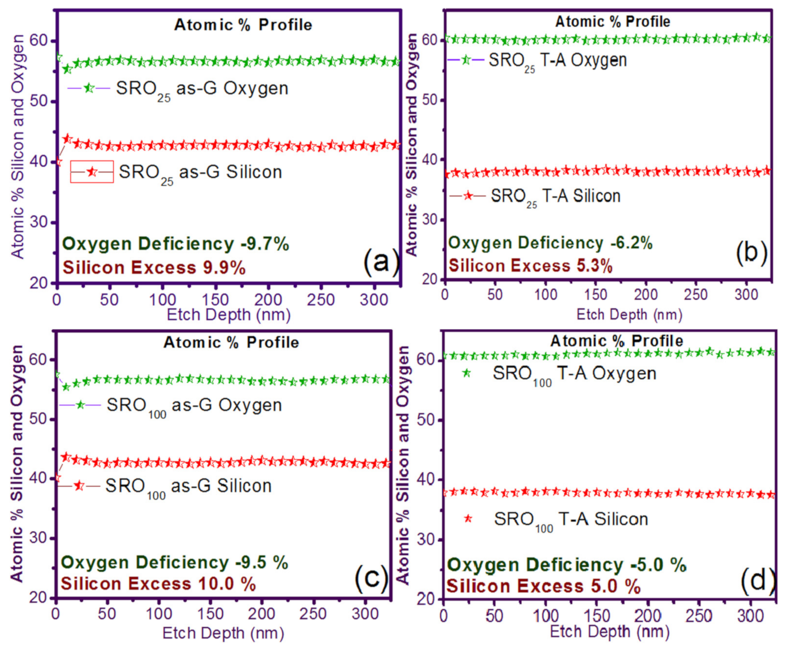
| Si/SRO25 | 322.9 | 2.46 ± 0.03 | −9.7 | 9.9 | 296.3 | 1.30 ± 0.04 | −6.2 | 5.3 |
| Q/Pn+/SRO25 | 351.8 | 319.6 | ||||||
| Si/SRO100 | 319.6 | 2.04 ± 0.35 | −9.5 | 10.0 | 283.5 | 1.02 ± 0.08 | −5.0 | 5.0 |
| Q/Pn+/SRO100 | 339.0 | 306.6 | ||||||
| Si/SRO25/100 | 592.3 | 1.46 ± 0.06 | 583.3 | 1.93 ± 0.31 | ||||
| Q/QPn+/SRO25/100 | 654.3 | 611.7 | ||||||
| Si/SRO100/25 | 578.9 | 1.51 ± 0.002 | 560.5 | 2.05 ± 0.65 | ||||
| Q/QPn+SRO100/25 | 668.2 | 599.3 | ||||||
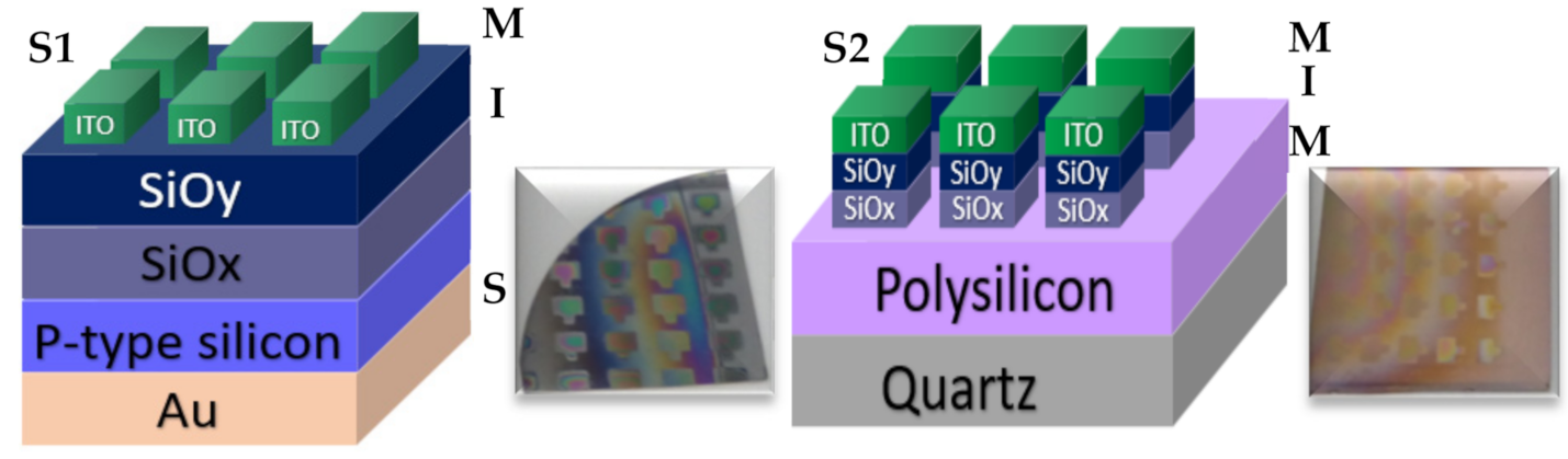
| Structure 1 (S1) | Mnemonics | Structure 2 (S2) | Mnemonics |
|---|---|---|---|
| MIS | MIM | ||
| Au/Si/SRO25as-G/ITO | S125as-G | Q/Pn+/SRO25as-G/ITO | S225as-G |
| Au/Si/SRO100as-G/ITO | S1100as-G | Q/Pn+/SRO100as-G/ITO | S2100as-G |
| Au/Si/SRO25/100as-G/ITO | S125/100as-G | Q/Pn+/SRO25/100as-G/ITO | S225/100as-G |
| Au/Si/SRO100/25as-G/ITO | S1100/25as-G | Q/Pn+/SRO100/25as-G/ITO | S2100/25as-G |
| Au/Si/SRO25T-A/ITO | S125T-A | Q/Pn+/SRO10T-A/AZO | S225T-A |
| Au/Si/SRO100T-A/ITO | S1100T-A | Q/Pn+/SRO25T-A/AZO | S2100T-A |
| Au/Si/SRO25/100T-A/ITO | S125/100T-A | Q/Pn+/SRO25/10T-A/AZO | S225/100T-A |
| Au/Si/SRO100/25T-A/ITO | S1100/25T-A | Q/Pn+/SRO10/25T-A/AZO | S2100/25T-A |
Publisher’s Note: MDPI stays neutral with regard to jurisdictional claims in published maps and institutional affiliations. |
© 2021 by the authors. Licensee MDPI, Basel, Switzerland. This article is an open access article distributed under the terms and conditions of the Creative Commons Attribution (CC BY) license (http://creativecommons.org/licenses/by/4.0/).
Share and Cite
Martínez, H.P.; Luna, J.A.; Morales, R.; Casco, J.F.; Hernández, J.A.D.; Luna, A.; Hernández, Z.J.; Mendoza, G.; Monfil, K.; Ramírez, R.; et al. Blue Electroluminescence in SRO-HFCVD Films. Nanomaterials 2021, 11, 943. https://doi.org/10.3390/nano11040943
Martínez HP, Luna JA, Morales R, Casco JF, Hernández JAD, Luna A, Hernández ZJ, Mendoza G, Monfil K, Ramírez R, et al. Blue Electroluminescence in SRO-HFCVD Films. Nanomaterials. 2021; 11(4):943. https://doi.org/10.3390/nano11040943
Chicago/Turabian StyleMartínez, Haydee P., José A. Luna, Roberto Morales, José F. Casco, José A. D. Hernández, Adan Luna, Zaira J. Hernández, Gabriel Mendoza, Karim Monfil, Raquel Ramírez, and et al. 2021. "Blue Electroluminescence in SRO-HFCVD Films" Nanomaterials 11, no. 4: 943. https://doi.org/10.3390/nano11040943
APA StyleMartínez, H. P., Luna, J. A., Morales, R., Casco, J. F., Hernández, J. A. D., Luna, A., Hernández, Z. J., Mendoza, G., Monfil, K., Ramírez, R., Carrillo, J., & Flores, J. (2021). Blue Electroluminescence in SRO-HFCVD Films. Nanomaterials, 11(4), 943. https://doi.org/10.3390/nano11040943