
Wafer-Scale Epitaxial Low Density InAs/GaAs Quantum Dot for Single Photon Emitter in Three-Inch Substrate

 ,
, 
Abstract
1. Introduction
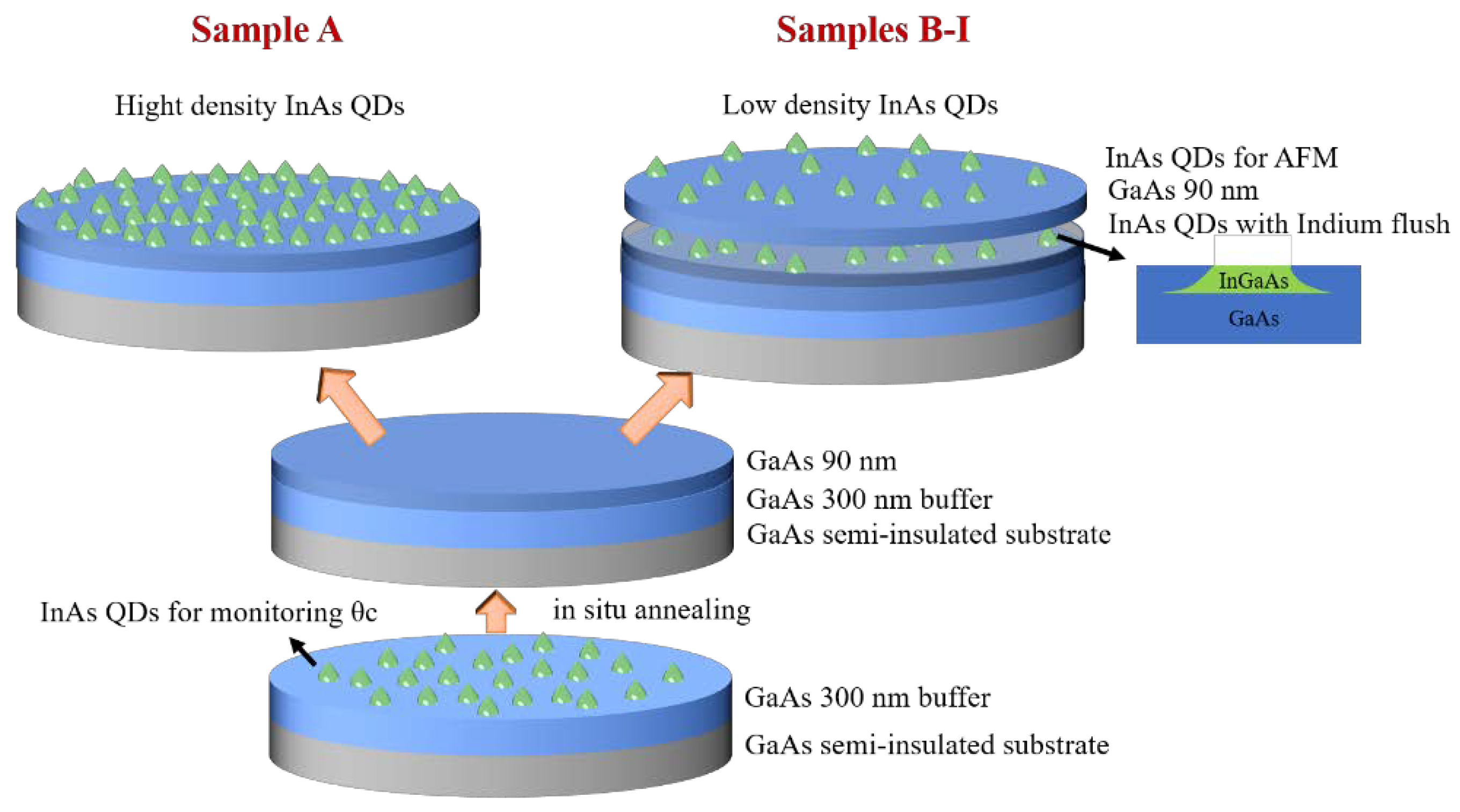
2. Method
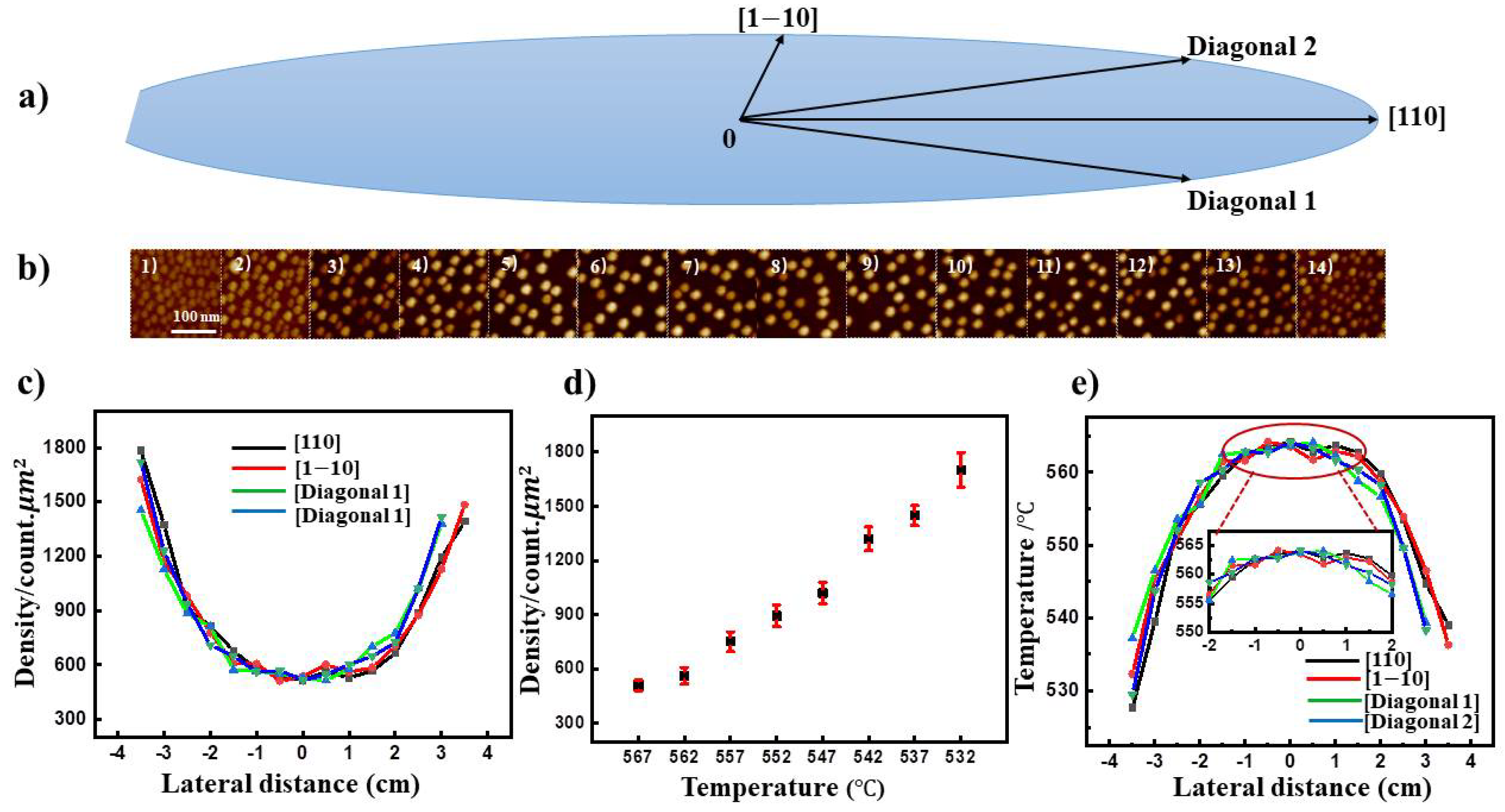
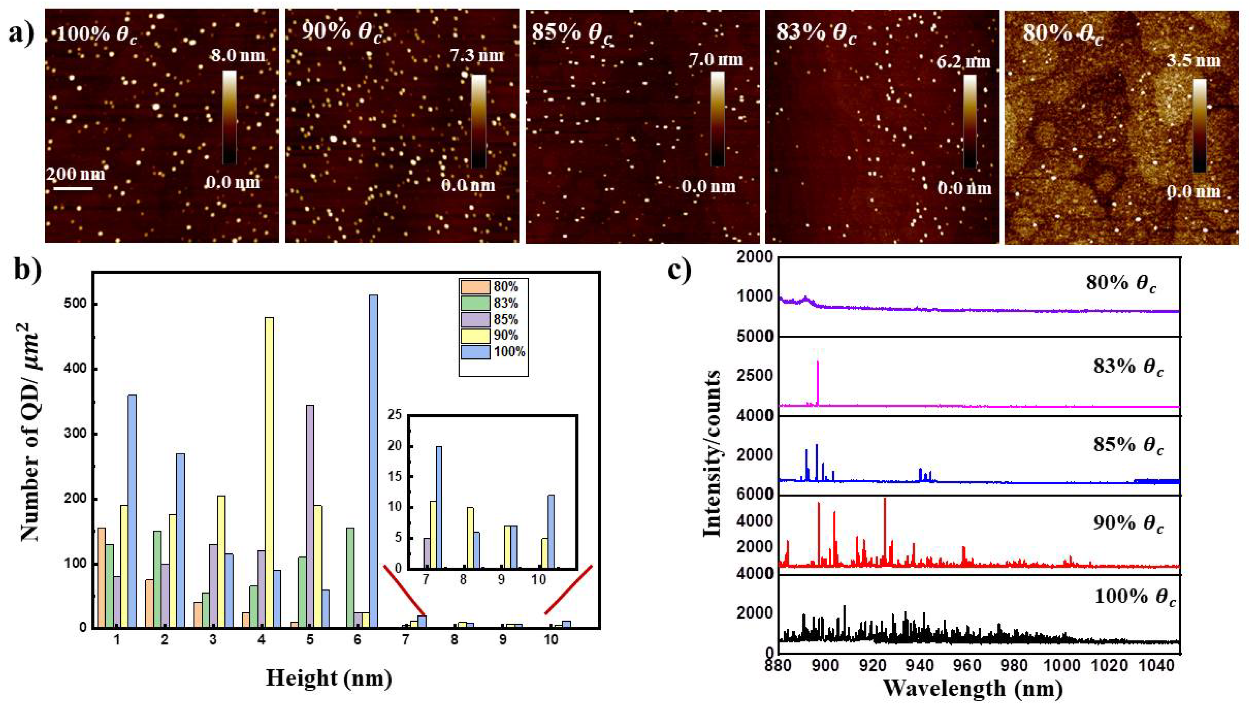
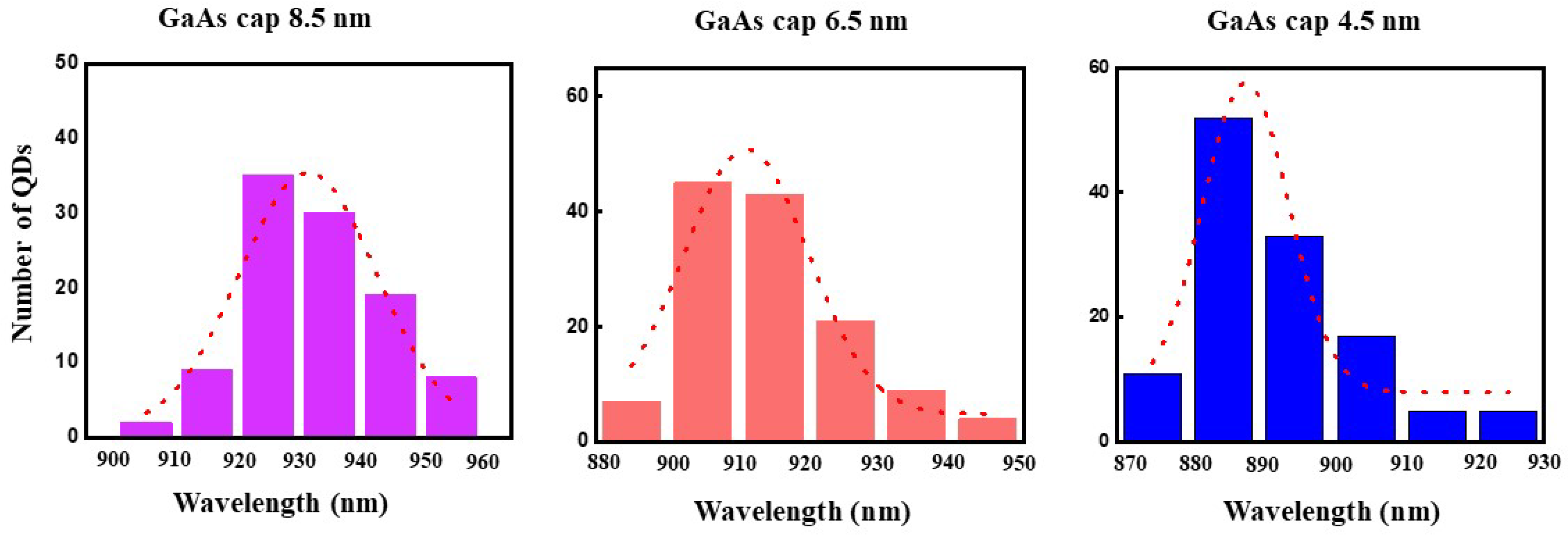
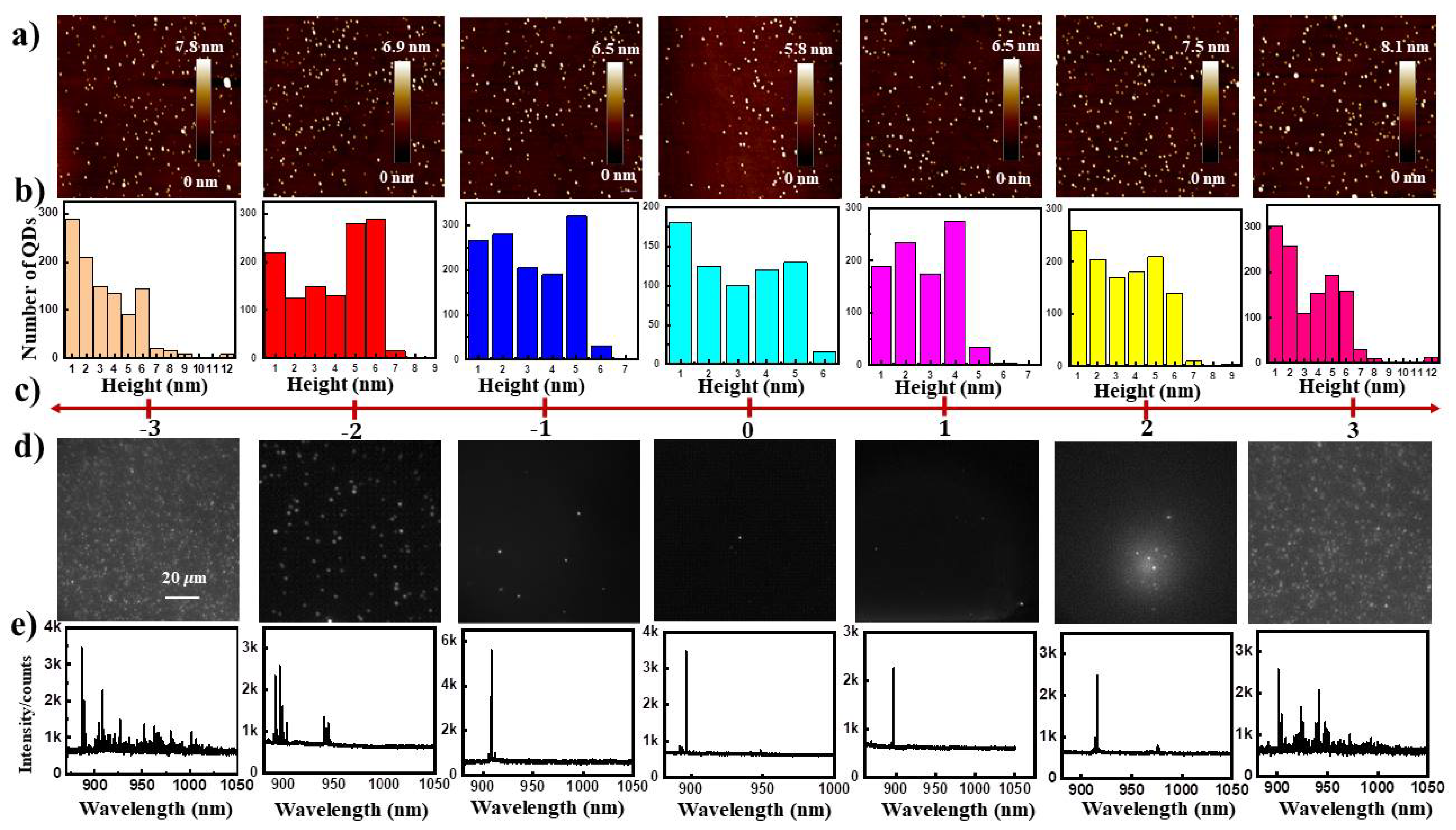
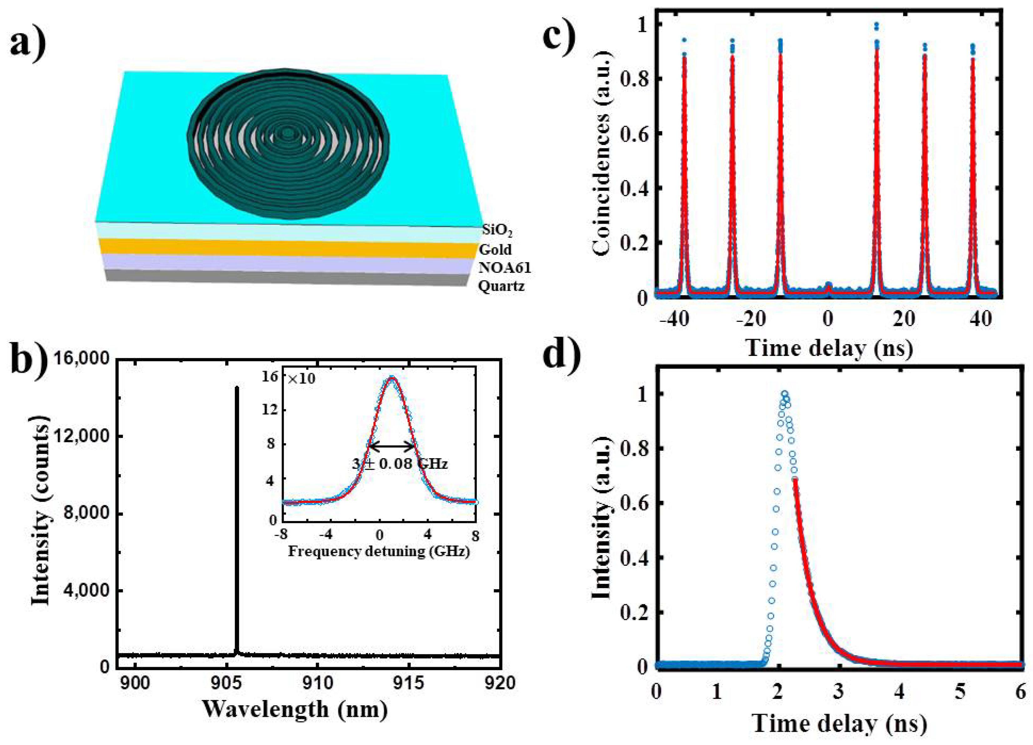
3. Results and Discussion
4. Conclusions
Supplementary Materials
Author Contributions
Funding
Data Availability Statement
Conflicts of Interest
References
- Majid, M.A.; Childs, D.T.D.; Kennedy, K.; Clarke, E.; Murray, R.; Airey, R.; Hogg, R.A.; Spencer, P. Strain engineered bilayers for extending the operating wavelength of quantum dot lasers. IET Optoelectron. 2011, 5, 100–104. [Google Scholar] [CrossRef]
- Shi, J.-J.; Dong, W.; Xu, Y.-Z.; Li, C.-H.; Lv, S.-T.; Zhu, L.-F.; Dong, J.; Luo, Y.-H.; Li, D.-M.; Meng, Q.-B.; et al. Enhanced Performance in Perovskite Organic Lead Iodide Heterojunction Solar Cells with Metal-Insulator-Semiconductor Back Contact. Chin. Phys. Lett. 2013, 30, 128402. [Google Scholar] [CrossRef]
- Dongre, S.; Paul, S.; Mondal, S.; Panda, D.; Shriram, S.R.; Mantri, M.R.; Gazi, S.A.; Das, D.; Kumar, R.; Tongbram, B.; et al. Optimization of vertical strain coupling in InAs/GaAs p-i-p quantum dot infrared photodetectors with applied growth strategy. J. Lumin. 2020, 226, 117499. [Google Scholar] [CrossRef]
- Kupko, T.; von Helversen, M.; Rickert, L.; Schulze, J.-H.; Strittmatter, A.; Gschrey, M.; Rodt, S.; Reitzenstein, S.; Heindel, T. Tools for the performance optimization of single-photon quantum key distribution. NPJ Quantum Inf. 2020, 6, 29. [Google Scholar] [CrossRef]
- Pirandola, S.; Andersen, U.L.; Banchi, L.; Berta, M.; Wallden, P. Advances in Quantum Cryptography. Adv. Opt. Photonics 2020, 12, 1012–1236. [Google Scholar] [CrossRef]
- Korzh, B.; Lim, C.C.W.; Houlmann, R.; Gisin, N.; Li, M.J.; Nolan, D.; Sanguinetti, B.; Thew, R.; Zbinden, H. Provably secure and practical quantum key distribution over 307 km of optical fibre. Nat. Photonics 2015, 9, 163–168. [Google Scholar] [CrossRef]
- Bentham, C.; Hallett, D.; Prtljaga, N.; Royall, B.; Vaitiekus, D.; Coles, R.J.; Clarke, E.; Fox, A.M.; Skolnick, M.S.; Itskevich, I.E.; et al. Single-photon electroluminescence for on-chip quantum networks. Appl. Phys. Lett. 2016, 109, 161101. [Google Scholar] [CrossRef]
- Huber, D.; Reindl, M.; Huo, Y.; Huang, H.; Wildmann, J.S.; Schmidt, O.G.; Rastelli, A.; Trotta, R. Highly indistinguishable and strongly entangled photons from symmetric GaAs quantum dots. Nat. Commun. 2017, 8, 15506. [Google Scholar] [CrossRef]
- Chia, C.K.; Zhang, Y.W.; Wong, S.S.; Chua, S.J.; Yong, A.M.; Chow, S.Y. Testing the upper limit of InAs/GaAs self-organized quantum dots density by fast growth rate. Superlattices Microstruct. 2008, 44, 420–424. [Google Scholar] [CrossRef]
- Heyn, C.; Stemmann, A.; Koeppen, T.; Strelow, C.; Kipp, T.; Grave, M.; Mendach, S.; Hansen, W. Highly uniform and strain-free GaAs quantum dots fabricated by filling of self-assembled nanoholes. Appl. Phys. Lett. 2009, 94, 183113. [Google Scholar] [CrossRef]
- Herranz, J.; González, L.; Wewior, L.; Alén, B.; Fuster, D.; González, Y. Study of Growth Parameters for Single InAs QD Formation on GaAs(001) Patterned Substrates by Local Oxidation Lithography. Cryst. Growth Des. 2014, 15, 666–672. [Google Scholar] [CrossRef]
- Scholz, S.; Schott, R.; Schmidt, M.; Mehta, M.; Ludwig, A.; Wieck, A.D. Self-Organized Growth of Quantum Dots and Quantum Wires by Combination of Focused Ion Beams and Molecular Beam Epitaxy. Phys. Status Solidi 2018, 256, 1800375. [Google Scholar] [CrossRef]
- Martín-Sánchez, J.; Muñoz-Matutano, G.; Herranz, J.; Canet-Ferrer, J.; Alén, B.; González, Y.; Alonso-González, P.; Fuster, D.; González, L.; Martínez-Pastor, J.; et al. Single Photon Emission from Site-Controlled InAs Quantum Dots Grown on GaAs(001) Patterned Substrates. ACS Nano 2009, 3, 1513–1517. [Google Scholar] [CrossRef] [PubMed]
- Kalyuzhnyy, N.A.; Mintairov, S.A.; Salii, R.A.; Nadtochiy, A.M.; Payusov, A.S.; Brunkov, P.N.; Nevedomsky, V.N.; Shvarts, M.Z.; Martí, A.; Andreev, V.M.; et al. Increasing the quantum efficiency of InAs/GaAs QD arrays for solar cells grown by MOVPE without using strain-balance technology. Prog. Photovolt. Res. Appl. 2016, 24, 1261–1271. [Google Scholar] [CrossRef]
- Wang, S.Y.; Ling, H.S.; Lee, C.P. Temperature dependence of quantum efficiency in Quantum Dot Infrared Photodetectors. Infrared Phys. Technol. 2011, 54, 224–227. [Google Scholar] [CrossRef]
- Pedersen, F.T.; Wang, Y.; Olesen, C.T.; Scholz, S.; Wieck, A.D.; Ludwig, A.; Löbl, M.C.; Warburton, R.J.; Midolo, L.; Uppu, R.; et al. Near Transform-Limited Quantum Dot Linewidths in a Broadband Photonic Crystal Waveguide. ACS Photonics 2020, 7, 2343–2349. [Google Scholar] [CrossRef]
- Sameshima, K.; Sano, T.; Yamaguchi, K. Self-formation of ultrahigh-density (1012 cm−2) InAs quantum dots on InAsSb/GaAs(001) and their photoluminescence properties. Appl. Phys. Express 2016, 9, 075501. [Google Scholar] [CrossRef]
- Huang, S.; Niu, Z.; Ni, H.; Xiong, Y.; Zhan, F.; Fang, Z.; Xia, J. Fabrication of ultra-low density and long-wavelength emission InAs quantum dots. J. Cryst. Growth 2007, 301, 751–754. [Google Scholar] [CrossRef]
- Shang, X.J.; Xu, J.X.; Ma, B.; Chen, Z.S.; Wei, S.H.; Li, M.F.; Zha, G.W. Proper In deposition amount for on-demand epitaxy of InAs/GaAs single quantum dots. Chin. Phys. B 2016, 25, 448–454. [Google Scholar] [CrossRef]
- Garcia, A.; Mateo, C.M.; Defensor, M.; Salvador, A.; Philpott, E. Influence of As4 flux on the growth kinetics, structure, and optical properties of InAs /GaAs quantum dots. J. Appl. Phys. 2007, 102, 073526. [Google Scholar] [CrossRef]
- Li, S.; Chen, Q.; Sun, S.; Li, Y.; Fang, Y. InAs/GaAs quantum dots with wide-range tunable densities by simply varying V/III ratio using metal-organic chemical vapor deposition. Nanoscale Res. Lett. 2013, 8, 367. [Google Scholar] [CrossRef]
- Sun, J.; Jin, P.; Wang, Z.-G. Extremely low density InAs quantum dots realized in situ on (100) GaAs. Nanotechnology 2004, 15, 1763–1766. [Google Scholar] [CrossRef]
- Yu, Y.; Shang, X.J.; Li, M.F.; Zha, G.W. Single InAs quantum dot coupled to different “environments” in one wafer for quantum photonics. Appl. Phys. Lett. 2013, 102, 2418. [Google Scholar] [CrossRef]
- Huang, X.; Zhong, H.; Yang, J.; Liu, L.; Liu, J.; Yu, Y.; Yu, S. Morphological engineering of aluminum droplet etched nanoholes for symmetric GaAs quantum dot epitaxy. Nanotechnology 2020, 31, 495701. [Google Scholar] [CrossRef]
- Patella, F.; Arciprete, F.; Fanfoni, M.; Balzarotti, A.; Placidi, E. Apparent critical thickness versus temperature for InAs quantum dot growth on GaAs(001). Appl. Phys. Lett. 2006, 88, 081305. [Google Scholar] [CrossRef]
- Li, M.F.; Yu, Y.; He, J.F.; Wang, L.J.; Zhu, Y.; Shang, X.J.; Ni, H.Q.; Niu, Z.C. In situ accurate control of 2D-3D transition parameters for growth of low-density InAs/GaAs self-assembled quantum dots. Nanoscale Res. Lett. 2013, 8, 86. [Google Scholar] [CrossRef] [PubMed]
- Chen, Z.S.; Ma, B.; Shang, X.J.; He, Y.; Zhang, L.C.; Ni, H.Q.; Wang, J.L.; Niu, Z.C. Telecommunication Wavelength-Band Single-Photon Emission from Single Large InAs Quantum Dots Nucleated on Low-Density Seed Quantum Dots. Nanoscale Res. Lett. 2016, 11, 382. [Google Scholar] [CrossRef][Green Version]
- Sasakura, H.; Kayamori, S.; Adachi, S.; Muto, S. Effect of indium-flush method on the control of photoluminescence energy of highly uniform self-assembled InAs quantum dots by slow molecular beam epitaxy growth. J. Appl. Phys. 2007, 102, 013515. [Google Scholar] [CrossRef]
- Reithmaier, J.P.; Riechert, H.; Schl?Tterer, H.; Weimann, G. Indium desorption during MBE growth of strained InGaAs layers. J. Cryst. Growth 1991, 111, 407–412. [Google Scholar] [CrossRef]
- Ying, W.; Xinzhi, S.; Yao, L.; Baolai, L.; Xiaoli, L.; Qinglin, G.; Mazur, Y.I.; Ware, M.E.; Salamo, G.J. PL of low-density InAs/GaAs quantum dots with different bimodal populations. IET Micro Nano Lett. 2017, 12, 599–604. [Google Scholar]
- Rezgui, K.; Othmen, R.; Cavanna, A.; Ajlani, H.; Madouri, A.; Oueslati, M. The improvement of InAs/GaAs quantum dot properties capped by Graphene. J. Raman Spectrosc. 2013, 44, 1529–1533. [Google Scholar] [CrossRef]
- Lee, J.S.; Ren, H.W.; Sugou, S.; Masumoto, Y. In0.5Ga0.5As quantum dot intermixing and evaporation in GaAs capping layer growth. J. Appl. Phys. 1998, 84, 6686–6688. [Google Scholar] [CrossRef]
- Alloing, B.; Zinoni, C.; Zwiller, V.; Li, L.H.; Monat, C.; Gobet, M.; Buchs, G.; Fiore, A.; Pelucchi, E.; Kapon, E. Growth and characterization of single quantum dots emitting at 1300 nm. Appl. Phys. Lett. 2005, 86, 101908. [Google Scholar] [CrossRef]
- Sapienza, L.; Davanço, M.; Badolato, A.; Srinivasan, K. Nanoscale optical positioning of single quantum dots for bright and pure single-photon emission. Nat. Commun. 2015, 6, 7833. [Google Scholar] [CrossRef]
- Yao, B.; Su, R.; Wei, Y.; Liu, Z.; Zhao, T.; Liu, J. Design for Hybrid Circular Bragg Gratings for a Highly Efficient Quantum-Dot Single-Photon Source. J. Korean Phys. Soc. 2018, 73, 1502–1505. [Google Scholar] [CrossRef]
- Liu, J.; Su, R.; Wei, Y.; Yao, B.; Silva, S.; Yu, Y.; Iles-Smith, J.; Srinivasan, K.; Rastelli, A.; Li, J.; et al. A solid-state source of strongly entangled photon pairs with high brightness and indistinguishability. Nat. Nanotechnol. 2019, 14, 586–593. [Google Scholar] [CrossRef]
- Liu, J.; Konthasinghe, K.; Davanço, M.; Lawall, J.; Anant, V.; Verma, V.; Mirin, R.; Nam, S.W.; Song, J.D.; Ma, B.; et al. Srinivasan, Single self-assembled InAs/GaAs quantum dots in photonic nanostructures: The role of nanofabrication. Phys. Rev. Appl. 2018, 9, 064019. [Google Scholar] [CrossRef] [PubMed]


| Sample ID | Tc Thermocouple (°C) | T (InAs)/ Thermocouple (°C) | Thickness of GaAs Cap Layer (nm) | In Deposited Rate (ML/s) | In Deposited Amount | As Flux (Torr) |
|---|---|---|---|---|---|---|
| A | 602 | 562 | 0 | 0.08 | 150% | 1.8 × 10⁻⁶ |
| B | 605 | 580 | 8.5 | 0.004 | 100% | 5 × 10⁻⁷ |
| C | 603 | 578 | 8.5 | 0.004 | 90% | 5 × 10⁻⁷ |
| D | 603 | 578 | 8.5 | 0.004 | 85% | 5 × 10⁻⁷ |
| E | 605 | 580 | 8.5 | 0.004 | 83% | 5 × 10⁻⁷ |
| F | 602 | 577 | 8.5 | 0.004 | 80% | 5 × 10⁻⁷ |
| G | 600 | 575 | 6.5 | 0.004 | 83% | 5 × 10⁻⁷ |
| H | 605 | 580 | 4.5 | 0.004 | 83% | 5 × 10⁻⁷ |
| I | 605 | 580 | 2.5 | 0.004 | 83% | 5 × 10⁻⁷ |
| T (Calibration)/°C | T (InAs)/Thermocouple (°C) | In Deposited Rate (ML/s) | As Flux (Torr) | InAs Deposited Amount/ML |
|---|---|---|---|---|
| (Tc-40) °C | 562 | 0.004 | 5 × 10⁻⁷ | 1.60 |
| (Tc-30) °C | 572 | 0.004 | 5 × 10⁻⁷ | 1.67 |
| (Tc-25) °C | 577 | 0.004 | 5 × 10⁻⁷ | 1.86 |
| (Tc-20) °C | 582 | 0.004 | 5 × 10⁻⁷ | 1.92 |
| (Tc-15) °C | 587 | 0.004 | 5 × 10⁻⁷ | Not appear |
Publisher’s Note: MDPI stays neutral with regard to jurisdictional claims in published maps and institutional affiliations. |
© 2021 by the authors. Licensee MDPI, Basel, Switzerland. This article is an open access article distributed under the terms and conditions of the Creative Commons Attribution (CC BY) license (https://creativecommons.org/licenses/by/4.0/).
Share and Cite
Huang, X.; Su, R.; Yang, J.; Rao, M.; Liu, J.; Yu, Y.; Yu, S. Wafer-Scale Epitaxial Low Density InAs/GaAs Quantum Dot for Single Photon Emitter in Three-Inch Substrate. Nanomaterials 2021, 11, 930. https://doi.org/10.3390/nano11040930
Huang X, Su R, Yang J, Rao M, Liu J, Yu Y, Yu S. Wafer-Scale Epitaxial Low Density InAs/GaAs Quantum Dot for Single Photon Emitter in Three-Inch Substrate. Nanomaterials. 2021; 11(4):930. https://doi.org/10.3390/nano11040930
Chicago/Turabian StyleHuang, Xiaoying, Rongbin Su, Jiawei Yang, Mujie Rao, Jin Liu, Ying Yu, and Siyuan Yu. 2021. "Wafer-Scale Epitaxial Low Density InAs/GaAs Quantum Dot for Single Photon Emitter in Three-Inch Substrate" Nanomaterials 11, no. 4: 930. https://doi.org/10.3390/nano11040930
APA StyleHuang, X., Su, R., Yang, J., Rao, M., Liu, J., Yu, Y., & Yu, S. (2021). Wafer-Scale Epitaxial Low Density InAs/GaAs Quantum Dot for Single Photon Emitter in Three-Inch Substrate. Nanomaterials, 11(4), 930. https://doi.org/10.3390/nano11040930