Abstract
One-dimensional metal nanowires, with novel functionalities like electrical conductivity, optical transparency and high mechanical stiffness, have attracted widespread interest for use in applications such as transparent electrodes in optoelectronic devices and active components in nanoelectronics and nanophotonics. In particular, silver nanowires (AgNWs) have been widely researched owing to the superlative thermal and electrical conductivity of bulk silver. Herein, we present a detailed review of the synthesis of AgNWs and their utilization in fabricating improved transparent conducting electrodes (TCE). We discuss a range of AgNW synthesis protocols, including template assisted and wet chemical techniques, and their ability to control the morphology of the synthesized nanowires. Furthermore, the use of scalable and cost-effective solution deposition methods to fabricate AgNW based TCE, along with the numerous treatments used for enhancing their optoelectronic properties, are also discussed.
1. Introduction
One-dimensional (1D) metal nanomaterials have attracted widespread research interest due to their unique electrical, magnetic, optical, thermal and catalytic properties. Consequently, such nanomaterials have become promising candidates for a wide range of applications in optoelectronics, nanoelectronics, nanophotonics and micromechanics because of their exceptional density of states and high aspect ratio [1,2,3,4,5]. In particular, silver (Ag) has the highest electrical and thermal conductivities of all metals, and its 1D form, referred to as Ag nanowires (AgNWs), has huge potential for practical applicability in a range of technologies. Over the years, numerous AgNW synthesis protocols have been proposed, including the use of soft and hard templates and a range of wet-chemical techniques like hydrothermal, solvothermal and polyol-based synthesis. This has resulted in wide range of achievable dimensions (diameter 2–300 nm and length 1–500 µm). A relative comparison on the bases of simplicity, control, yield and cost demonstrated that the polyol process is the most promising method for AgNW synthesis. Research in the area of AgNWs has been extensive, with over 100,000 publications covering a vast range of applications including smart sensors [6,7,8,9,10], catalysis [11], energy harvesting devices [12], optoelectronic displays [13] and wearable electronics [14,15,16], among others. Furthermore, theoretical predictions and experimental demonstrations have highlighted the fact that AgNWs can significantly improve the properties of transparent conducting electrodes (TCE), which are an essential component of optoelectronic devices. Traditionally the material of choice for fabricating TCE has been indium tin oxide (ITO) due to its low sheet resistance, high optical transmittance, low surface roughness and ability to pattern electrodes using photolithography. However, ITO has various drawbacks, including its high fabrication cost and brittle nature, which hinders its applicability for use in next-generation flexible optoelectronic devices like smart windows [17,18], electronic skins [19], smart clothes [20], wearable heaters [21,22], foldable displays [23,24,25,26], compliant solar cells [27] and flexible display panels [28]. These devices require TCE that fulfill certain criteria, including solution-based low cost processing capability, excellent optoelectronic properties, mechanical compliance and chemical stability. A variety of alternatives to ITO, such as carbon nanotubes (CNTs), graphene oxide (GO), aluminum zinc oxide (AZO), metal nanowires, nanofibers and conductive polymers have been reported for TCE fabrication. In particular, AgNW based TCE have emerged as a perfect contender for modern optoelectronic and wearable devices due their low-cost and scalable solution based processing, high conductivity and transparency, smooth surface and mechanical flexibility [16,29,30,31,32,33,34,35,36,37]. AgNWs can be deposited on various substrates and form a network with openings between the nanowires that allow light transmittance while conductive pathways are formed at the nanowire junctions.
Herein, we have compiled and presented a detailed review of AgNW synthesis and strategies for AgNW based TCE fabrication. A schematically illustrated outline of the review is presented in Figure 1. To the best of our knowledge, this is the first review that discusses all solution based TCE fabrication methods in detail and provides a comprehensive outlook of the various treatment techniques utilized to improve TCE performance. Briefly, this review is structured in the following manner: Section 1 introduces AgNWs and their utilization for TCE fabrication. Section 2 discusses the numerous AgNW synthesis methods, including template assisted and wet chemical techniques. Section 3 discusses the various solution-based methods used for TCE fabrication. In addition, it also provides a detailed analysis of the various pre- and post-treatment methods used to improve the optoelectronic properties of the fabricated TCE. Finally, outlooks and challenges for the practical applicability of AgNWs are presented.
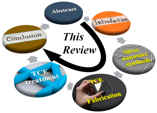
Figure 1.
Schematic illustration of the review outline.
2. AgNW Synthesis
Over the years, several protocols for AgNW synthesis have been reported. The use of templates, such as hard and soft templates, were widely investigated in the early years of AgNW synthesis. While predefined dimensions of the template assist in uniform nanowire synthesis, purification methods are quite complex and result in low yields. To overcome these issues, various wet chemical methods such as hydrothermal, solvothermal and polyol were later introduced. Among these, the polyol method has gathered much attention, since it is facile, scalable and provides good control over nanowire morphology. In this section, first, we will discuss the template methods, followed by the wet chemical methods. A Table 1 summarizing the various synthesis protocols is also added in the end of this section to provide a concise comparison and improve readability.

Table 1.
Summarized table of AgNW synthesis methods.
2.1. Template Methods
Researchers have utilized a range of templates that enable the growth of 0-D nanoparticles into 1-D nanowires. These templates are generally used to provide a specific size and structure to the nanowire [38]. These templates can be broadly categorized as either hard or soft. Hard templates result in greater control over the shape, size and overall morphology of the nanowire because of their predesigned structure that shapes the Ag atoms into nanowires. Although simple and effective, there can be significant loss of generated nanowires during the purification step, leading to lower yields. On the other hand, soft template methods utilize chemicals which are dispersible/dissolvable in solvents. Consequently, the synthesized nanowires can be easily purified from the solvent phase, thus resulting in improved efficiency and scalability.
2.1.1. Hard Template Method
The hard-template method utilizes a material of nanoscale porosity, which primarily serves as a template for the targeted material to grow in a well-designed manner. The template materials can be nanoporous polymers, carbon nanotubes (CNT), nonporous silica [39] and zeolites, which direct the germination and synthesis of AgNWs [40,41,42,43]. The idea of using host matrices of CNT was first introduced by Ajayan [40]. They first annealed the CNT in the presence of liquid lead, which opened the capped tube ends, and then filled these tubes with molten silver through capillary action. Following the same path, Ugarte et al. [41] described a new way to fill the CNT with silver to produce AgNWs having a length of 120 nm. Silver nitrate (AgNO3) salt was thermolyzed by an electron irradiation beam to obtain pure molten silver, which was injected into the CNT under high pressure to form nanowires. Han and coworkers demonstrated a simple procedure for the formation of nanowires using mesoporous silica SBA-15 as the template [42]. The growth direction and diameter of AgNW was easy to control in this method due to the highly ordered pore size distribution of SBA-15. Takai et al. also synthesized AgNWs with the help of mesoporous silica (SBA-15) powders and dimethyl-amine borane (DMAB) as the reducing agent [43]. This enabled the AgNWs to grow in the micro pores of the SBA-15 by capillary force under low pressure as schematically shown in Figure 2a. The SBA-15 templating method can be used to produce AgNWs with aspect ratios greater than 500 (L = 4 µm, D = 7 nm) as shown in the TEM images in Figure 2f,g [44].
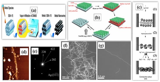
Figure 2.
(a) A Schematic procedure for AgNW synthesis using Mesoporous Silica (SBA-15) through Vapor Infiltration Method (adapted from [43] with permission from ACS publications, 2010.) (b) A procedure for AgNW arrays growth within AAO template (adapted from [54] with permission from Elsevier, 2020). (c) A Schematic for AgNW synthesis using λ-DNA (C1), Silver-ion-loading on DNA Bridge. (C2), Metallic silver aggregates bound to the DNA skeleton. (C3), fully developed silver wire after HQ reduction. (d) Atomic force microscopy (AFM) images (Dimension 3000, Digital Instruments) of a silver wire connecting two gold electrodes 12 µm apart (adapted from [49] with permission from Springer nature, 1998). (e) Selected area electron diffraction (SAED) of AgNWs synthesized using AAO template (adapted from [54] with permission from Elsevier, 2020). (f) SEM images of AgNWs and (g) Scanning electron microscopy (SEM) image of a single AgNW synthesized using SBA-15 template adapted from [44] with permission from Springer nature, 2012).
DNA has also been utilized a template due to its useful mechanical [45,46] and molecular recognition properties [47]. The mechanical properties allow it to make the required shape, alignment and junctions, while the recognition property improves the selectivity of Ag ions to form supramolecular structures [48]. A λ-DNA based template was introduced between two gold electrodes separated by a few micrometers; the resulting λ-DNA bridge could selectively choose the Ag ions by ion exchange process to form a wire-like structure [49]. A further addition of acidic hydroquinone solution reduced the Ag to form a more conductive aggregate. A schematic of the procedure is shown in Figure 2c, and the fabricated AgNWs with a length of 12–16 µm were characterized by AFM and fluorescence imaging, as shown in Figure 2d. Berti and coworkers also utilized a λ-DNA-template and photoreduction process to obtain silver composites and films [50]. The synthesized silver ions (Ag+) were embedded into the λ-DNA to form a complex, which, after photoreduction, was reduced to Ag nanoparticles, as confirmed by the peak observed at 420 nm using UV-VIS spectroscopy. Lu et al. demonstrated that sunlight could also be used for the reduction of silver ions to nanoparticles adsorbed on the surface of DNA [51]. Among all the templates, anodic aluminum oxide (AAO) is the most commonly used for nanowire synthesis [52,53]. In 2020, AAO templates were used to synthesize single crystalline AgNWs, as shown in Figure 2e [54]. The process used molten Ag and the AgNWs were grown in bundles at 970 °C under capillary action. Hydrothermal etching was later used to remove the AAO template using sodium hydroxide (NaOH) solution in a high pressure autoclave, as schematically illustrated in Figure 2b.
In summary, AgNW synthesis can be easily controlled to get the desired shape and size by the hard template method. Furthermore, the synthesized nanowires are already in a composite state, which can aid in practical applicability like device fabrication. However, to enable purification, dissolution of template is required, during which the AgNWs suffer from unfavorable conditions, and their high active surface energy often leads to damage in form of oxidation and etching.
2.1.2. Soft Template Methods
The quantity and quality of the synthesized nanowires via hard template methods is restricted to the porosity and interconnectivity of template. In addition, the harvesting step of nanowires is not viable for practical application at a large scale. Instead, the availability of soft template methods makes processing better and more efficient. Various amphiphilic compounds, such as calix-hydroquinone (CHQ), Supramolecular β-cyclodextrin (β-CD), cholesteryl pyridine carbamate (CPC) organogel, double-hydrophilic block copolymers (DHBC) and J-aggregate dye, support the generation of self-assembled templates for nanowire synthesis.
Hong and coresearchers used the soft template method to synthesize highly stable and single crystal ultrathin AgNWs with atomic dimensions (0.4 nm diameter) and length in the micrometer range. They used the pores of CHQ, because HQs are known for their reducing properties [55]. Ag ions were reduced to form silver aggregates by electro-/photochemical reaction in solution phase at ambient conditions (temperature and pressure). The synthesized nanowires could be kept in ambient temperature and pressure for one month with no change in the properties. The idea of using polymers as a soft template may also be viable due to the longer structural length of polymer. Hence, a novel approach for nanowire formation in a Poly-vinyl alcohol (PVA) film by electrodeposition was reported [56]. They performed two stage treatment of PVA film with ammonium persulphate [(NH4)2S2O8] and pyrrole (C4H4NH) to enable polymerization. Later, they soaked this film in a AgNO3 precursor solution, which acted as an electrolyte, and the nanowires grew in the nanoscale channels of the polymer via electrodeposition. Organogels, which is a 3-D cross-linked matrix composition of liquid organic phase, especially stimuli-responsive gels, have wide variety of effective utilization in targeted drug-delivery systems and biomaterials [57,58,59]. Researchers are interested is using these supramolecular gels as soft templates for AgNW synthesis [60,61]. In 2018, β-CD derived soft templates were used for synthesis of AgNWs in the presence of iron chloride (FeCl3) [60]. FeCl3 primarily helps in formation of longer nanowires by circumventing the oxidation of the AgNW surface. An optimized ratio of FeCl3 and AgNO3 (1:13.3) with a 0.23 M concentration of soft template yielded nanowires with a length of up to 20 µm and a diameter of about 65 nm, as shown in Figure 3a,b.
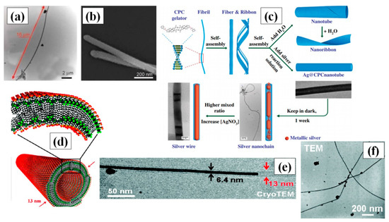
Figure 3.
(a) TEM images confirming the maximum width and length of the AgNWs (b) SEM image of synthesized AgNW (adapted from [60] with permission from Express Polymer Letters, 2018). (c) Schematic diagram of the formation of CPC nanotubes and their aid in AgNW growing via a classical mirror reaction (adapted from [59] with permission from John wiley and sons, 2004). (d) Illustrating the self-assembled double walled nanotubular J-aggregates dyes with an outer diameter of 13 nm (e) Transmission electron microscopy (TEM) image of a AgNW with a width of 6.4 nm partially filling a supramolecular dye nanotube, and a silver nanoparticle on the nanotube’s outside 15 min after adding AgNO3 to the solution, (f) TEM image of synthesized AgNWs using J-aggregate, (72 h after adding AgNO3) (adapted from [62] with permission from ACS publications, 2010).
Nguyen and Liu introduced a novel method in 2015 to synthesize long AgNWs via self-assembly of CPC [59]. The CPC was used to create highly stable nanotubes (longer than 100 micrometers) and acted as a soft template by providing the skeleton for the growth of AgNW through them in a gel of water and anisole. A schematic for the AgNW synthesis using CPC is depicted in Figure 3c. Although the AgNW synthesis was one-step, an optimized protocol with control over the AgNO3 concentration, reduction rate and gel synthesis ratio of water and anisole was extremely crucial for synthesis of long nanowires. Double-hydrophilic block copolymers (DHBC) consist of two hydrophilic polymers, whereby one interacts with the material and the other enhances the solubility [63]. Zhang et al., for the first time, used polymethyl methacrylate (PMMA) and polyethylene oxide (PEO) as DHBC for the synthesis of AgNWs at room temperature [64]. PEO enhanced the solubility of polymer in water solution and remained noninteractive with AgNO3, while PMMA helped in Ag reduction to form silver nanoparticles, which slowly grew into nanowires over time. J-aggregates are a special type of dye that have the property of supramolecular self-organization. Interestingly, some researchers use double-walled nanotubular J-aggregates of amphiphilic cyanine dyes as template, which self-assemble in a mixture of water and ethanol to form double walled nanotubes, as shown in Figure 3d [62]. These reversible J-aggregate soft templates provide the structure for nanowire growth in a very small diameter, i.e., less than 7 nm, as shown in the TEM image in Figure 3e,f, with the cyanine dye layer acting as the reducing agent for silver ions in photoinitiated conditions. The purification steps for the nanowires were quite easy due to the reversibility of soft template by surface passivation. These nanotubes provided more control over growth, and provided a better alternative for easy removal of the template after nanowire synthesis.
2.2. Chemical Methods
Most of the template methods are not efficient for scalable industrial production of AgNWs. This has encouraged researchers to think beyond existing templates and develop chemical synthesis methods that provide better control over the obtained morphology and avoid the template removal step. Chemical methods include solvents, surfactants, reducing and oxidizing agents to enable nanowires synthesis. The first stage of synthesis is nanocrystal formation in the solution, which later grows to form the nanorod (aspect ratio <10) or nanowire (aspect ratio ~101–104) structure. The process of synthesizing AgNWs and nanorods by Ag seed in controlled manner are quite similar which can be observed in Figure 4h,i. Ag seeds were synthesized by reducing AgNO3 in presence of Sodium borohydride (NaBH4) and trisodium citrate (Na3C6H5O7) where NaBH4 controls the particle size and Na3C6H5O7 stabilizes it. Later to synthesize nanowires and nanorods, ascorbic acid (AA) was used to reduce AgNO3 in a solution embedded with Ag seed, NaOH and the micelle template cetyltrimethylammoniun bromide (CTAB) [65]. The relative amount of NaOH in solution was the deciding factor for the synthesis of nanowires and nanorods. Since the optimized pH for nanorods and nanowires were 11.8 and 4.1 respectively, it suggests that the monoanion of ascorbic acid is the dominating factor in nanowire synthesis while the ascorbate dianion is an important factor in nanorod synthesis.
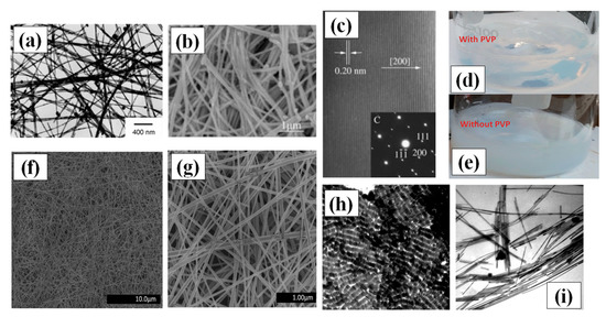
Figure 4.
(a) TEM images synthesized AgNWs using 1,3-bis(cetyldimethylammonium) propane dibromide (adapted from [73] with permission from Elsevier, 2006) (b) SEM image of the prepared AgNWs using glucose as reducing agents (adapted from [72] with permission from Chemistry-A European Journal, 2005). (c) A HRTEM image and single crystal SAED pattern of AgNWs (d–e) Digital camera images of solutions prepared for hydrothermal synthesis (d) with PVP in the form of hydrosol and (e) without PVP having precipitates in solution (f,g) The SEM images of uniform, ultralong and thin AgNWs prepared by the hydrothermal method at 160 °C for 22 h of reaction (adapted from [74] with permission from Royal Society of Chemistry, 2013) (h) TEM image of shape controlled silver nanorods (using pH~11); scale bar = 100 nm. (i) TEM image of AgNWs (using pH~11); scale bar = 100 nm (adapted from [65] with permission from Royal Society of Chemistry, 1996).
Sonochemical methods have also been used for the synthesis of AgNWs [66,67]. J.-J. Zhu et al. proposed a novel and seedless method for synthesis of Ag nanowires by a sonoelectrochemical method [68]. The electrochemical cell was composed of two platinum (Pt) sheets and an electrolyte composed of AgNO3 and ethylenediamine tetraacetic acid (EDTA) in water. The whole cell was kept in ultrasonic bath under nitrogen (N2) atmosphere with a current and voltage controlled electrolysis process for 30–45 min to grow AgNWs at 30 °C temperature. Another wet chemical synthesis method of AgNW interlacing bunches on glass walls by mild chemical reduction in aqueous solutions of PMAA was demonstrated [69]. Single-crystalline AgNWs with diameters of about 30–40 nm were synthesized inside the glass tube after 24 h at ambient temperature in the presence of AA as a reducing agent. Liu et al. introduced the idea of seed and crystals, where they first synthesized the silver bromide (AgBr) crystal seed which later grows into AgNWs with a maximum length of 9 µm [70].
2.2.1. Hydrothermal Methods
Hydrothermal synthesis methods consist of crystallizing the nanomaterial at high temperature and pressure in aqueous solution [71]. Hydrothermal methods for the synthesis of AgNWs are not widely applied these days, but in the first decade 21st century, hydrothermal processing produced the best nanowires. This method does not need any surfactant and copolymers as solvent or reducing agents. It is, therefore, a more favorable green chemistry route for growth of very long nanowires of length up to 500 µm without using any organic solvent or hazardous elements. Primarily, sodium chloride (NaCl) and AgNO3 are mixed in water to make silver chloride (AgCl). The Ag ions from AgCl are available during the growth process which lasted for 18 h at 180 °C in an autoclave [72]. Their idea of using glucose as a soft reducing agent is justified as it is also widely used for depositing silver films on glass substrate. The crystallinity and the growth direction of AgNW (perpendicular to the 200 plane) is shown in Figure 4c.
Xu and group demonstrated Ag nanowire synthesis by hydrothermal method at lower temperature (100 °C) in an autoclave with the help of 1,3-bis (cetyldimethylammonium) propane dibromide as the reducing agent over a time span of one day [73]. The problem assisted with the hydrothermal methods was precipitation of AgCl and Ag nanocrystals, which can be seen in Figure 4a,b. In order to avoid the precipitation effect, Bari et al. used Polyvinylpyrrolidone (PVP) as a surfactant and made hydrosol with water and D+ glucose, which enhanced the anisotropic growth property and morphology of the AgNWs [74]. The PVP addition results in a precipitationless solution (Figure 4d); however, without PVP, a precipitate appears, as seen in Figure 4e. The process involves drop wise addition of NaCl ions to promote the growth in a very stabilized and controlled way. They put the hydrosol in a stainless steel autoclave for 22 h at 160 °C. Very-long and thin AgNWs of length in the range of 200 to 500 µm with an average diameter of 45–65 nm were synthesized with a uniform surface as shown in Figure 4g,h.
2.2.2. Polyol Method
• Historical development
Among the available methods, the polyol method is the most widely utilized by researchers. Currently, there are more than 10,000 publications on AgNW synthesis using polyol method in last decade. Fievet et al. introduced the benefits of polyol process for metal nanostructure synthesis [75]. The reason for adopting this method is simplicity, cost effectiveness, mass production for industrial use and good output with better control over dimensions [76,77]. Ag nanomaterials may be generated in various shapes and sizes with great control over the dimensions using the polyol method by changing the parameters, such as concentration of precursor, capping agent, reducing agent, type of solvent, temperature, reaction time and surrounding conditions [78,79]. These nanostructures are mostly obtained via anisotropic growth of the particles, where not all the dimensions of the nanomaterial grow at the same rate. Silver nanorods and nanowires are typical examples of anisotropic growth of nanoparticles in one direction. For AgNWs synthesis at large scale, the polyol method uses silver nitrate as a precursor for the synthesis, PVP as a polymeric capping agent/surfactant and ethylene glycol (EG) as a reducing agent and solvent. Oxidation of silver is spontaneous and a major problem as reported previously [80,81] To avoid oxidation transition metal halide salts such as FeCl3, CuCl2, cobalt chloride (CoCl2), chromium chloride (CrCl2), are platinum chloride (PtCl2), are used. Where transition metal ions are first reduced by EG and later these metals scavenge the oxygen from silver nanocrystal surface while the Cl ions help in stabilizing the silver ions in such a way that they will be later available for the growth of AgNWs.
The first ever polyol method using EG was performed by Xia et al. in 2002 [82]. They synthesized bicrystalline nanowires of length 50 µm and aspect ratio ~1000, where EG acted as a reducing agent as well as a solvent. The synthesis process comprised two steps: Pt nanoparticles were used as seeds (1st step) for AgNWs growth (2nd step) due to their similar crystal structure, lattice constants and reduction conditions. They proposed that the silver ions start nucleation and unidirectional growth under the influence of PVP as the surfactant, while the unused Pt seeds are separated, as their size is very small. A systematic process of growth of nanowires, as proposed by Xia et al. later in the same year, is shown below [83]. As the method was not cost effective due to the use of platinum seeds, the same group gave an idea about the self-seeding process, where they show that in controlled conditions such as injection rate, continuous magnetic stirring and optimized AgNO3/PVP ratio, AgNO3 can be reduced to form Ag nanocrystals. These nanocrystals grow to form AgNW with the same size and aspect ratio without Pt seed [84]. It had been reported that an optimized addition of metal salts affects the morphology (shape and size) of the subsequent nanomaterial [85,86]. Addition of Fe+2/Fe+3 ions in ethylene glycol solution(EG) with PVP can continuously fluctuate between +2 and +3 oxidation state, thus reducing the supersaturation level and reaction rate [87]. Furthermore, addition of Cl− ions in the reaction help in stabilizing Ag+ by making AgCl nanocrystals whose solubility is less than solubility of AgNO3 in solution. Hence, Ag seeds are formed at a very slow rate and as a result of low solubility, Ag ions are also released at a slower rate in solution [88]. It must be noted that above-mentioned facts slow the reaction rate, which encourages the anisotropic growth of nanowires in a specific direction. The same concept was used to facilitate the growth of AgNWs where Fe3+ was reduced to Fe2+ by ethylene glycol. The reduced Fe2+ ion scavenges the oxygen effectively from the surface of silver nanocrystal to prevent their dissolution [89]. The concept of fluctuating oxidation states lead the group to perform the same experiment in presence of copper chloride (CuCl and CuCl2). Copper exists in in two stable states (Cu1+ and Cu2+), and all the proceeding were quite similar, with a reasonable mechanism of growth process [88]. Detailed growth procedure and influencing factors have been discussed in further detail in the coming sections.
• The growth mechanism of AgNWs
Even though many researchers have experimented with various parameters, some necessary features are primarily important for high quality AgNW synthesis by polyol method. Ensuring a slow reaction rate to slowly achieve the supersaturation state of existing Ag nuclei in the solution is a major focus [90]. The second feature is avoiding the oxidative etching of silver nanostructures by providing any type of oxygen scavenger in the process. Primarily, the process starts with reduction of AgNO3 by ethylene glycol to form Ag atoms. The reduction process continues until the supersaturation state of Ag atom is attained after which the nucleation process of the atom starts. In the presence of PVP as a surfactant, slow reduction rate and availability of Cl ions are the main reasons that prevent the Ag nanocrystal aggregation in the solution. Although various strategies for AgNW synthesis have been used, the growth process is still not completely understood [82,83,84]. A number of nanocrystal shapes can be generated in form of single crystal and twinned silver seeds. Although a minor change in kinetics of the reaction may lead to a big change in morphology of nanocrystals [90,91,92]. The desire to inhabit the minimum energy level state of every Ag atoms resulted in majority of the particle shapes being multiply twinned seeds [93]. The single crystals and single twinned further generates nanocubes, bipyramidal, nanospheres, nanotetrahedrals and nanoctahedrals as shown in Figure 5a. The multiply twinned decahedral has been proven to be the most thermodynamically stable shape [94,95]. Xia et al. proposed that for the growth of AgNW, there are two vital factors: PVP interaction with Ag nuclei and multiply twinned particles (MTP) with decahedral shape. They mentioned that a multiple twinned particle with five-fold symmetry has ten {111} facets at the boundary, which was favorable for the minimum energy state of the system, as confirmed by the TEM image of the synthesized nanowires shown in Figure 5c–e. There are five twin boundaries on both sides of the growing dimensions of the wire and the surface energy associated at twin boundaries is highest as compared to other spots. Consequently, most of the Ag atoms are attracted to these twin boundaries and results in selective crystallization. This causes the growth of particle in a specific direction to form the nanowire. They also mentioned that for every {111} facet, there exits {100} plane, which is perpendicular to the longest dimension of nanowire. The interaction between PVP and {111} facet is very less as compared to strong interaction with the {100} plane. This prevents the silver atoms to combine at {100} facets and allows the syndication with {111} facet as shown in Figure 5b [96]. Once the growth process of MTPs starts, the next problem encountered is the oxidative etching of MTP precursors. As MTP are highly vulnerable to oxidative etching due to the defects available in the structure which can be seen in Figure 5f [97]. Hence, the available oxygen molecule species selectively tries to occupy these spaces and this may result in complete etching of MTP from the surface. It must be noted that oxidative etching can be of good use if other shapes such as nanocubes, nanospheres, nanotriangular and nano-bipyramidal are required. However, specifically for AgNWs, oxygen scavengers are required for high quality synthesis. Researchers have been using various metal halide compounds, such as FeCl3, CuCl2, CoCl2, and CrCl2. Fe(III) and Cu(II) are the two mostly used oxygen scavengers. When FeCl3/CuCl2 is injected in EG solution at high temperature, it is reduced from Fe(III)/Cu(II) to Fe(II)/Cu(I) (Figure 5g,h). Now, both the ions cannot be reduced further in the existing condition and eagerly oxidize by scavenging the oxygen from Ag surface to get back to Fe(III)/Cu(II). Successively, the ions can be further reduced by the EG and the process continues to yield high quality nanowires. It is advisable to perform the experiment under noble gas inert conditions because in such conditions, there will be no oxygen available from outside for oxidative etching. However, the presence of halide ions (Cl−) are equally important, as they are required for electrostatic stabilization [98,99]. A significant decrease in the available Ag has been reported after addition of Cl− ions due to AgCl formation and a comparatively slow release time of Ag+ ions was observed. It should be noted that there are many ways to add Cl− ions, e.g., prior to the AgNO3, along with AgNO3, and using AgCl as a precursor [100,101,102]. Although many parameter modifications have been studied, the process of successive multiple growth (SMG) is unique. Successive multiple step is used to synthesize the ultralong nanowires, i.e., of length up to 400 µm [102]. The initially formed nanowires are used as seeds to grow longer nanowires in multiple steps. All the conditions resemble the polyol method except the addition of an extra nanowire solution that acts as a precursor. A schematic for successive multiple growth with SEM images is shown in Figure 5i–m.
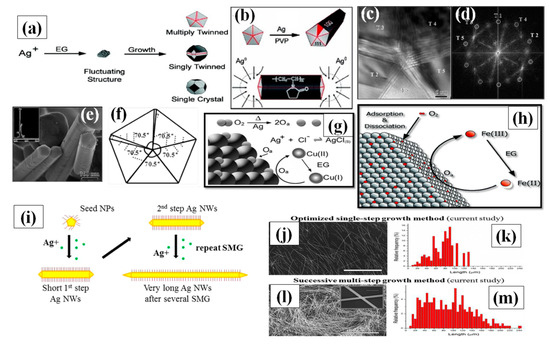
Figure 5.
(a) the process of Ag+ reduction and various types of seeds (multiply twinned, singly twinned, or single-crystal) formation in polyol method. Therefore, one must regulate the crystallinity of the seeds in a reaction to produce a specific shape. (b) Once twinned decahedral seeds lengthened into rods. PVP selectively adsorbed on the {100} side facets so that Ag atoms could only add to the {111} facets at the ends of each rod (adapted from [90] with permission from ACS publications, 2007). (c) HRTEM image of the center area of an Ag cross-section showing five distinctive {111} twinning boundaries, (scale bar 5 nm). (d) FFT image of Figure 5c (e) pentagonal profiles of the nanorods formed in initial stage of synthesis. The inset shows the EDX data from a nanorod. (f) Pentatetrahedral twin model for an Ag nanorod formation in initial stage (adapted from [97] with permission from ACS publications, 2004). (g) A schematic illustration depicting the role of Cu-containing salts in the polyol synthesis of AgNWs has been shown. Oxygen present during initial seed formation can adsorb and dissociate on the Ag seeds, blocking sites for further Ag deposition. Cu (I) rapidly scavenges this adsorbed atomic oxygen (O2), with the Cu(I) being oxidized to Cu(II). Ethylene glycol (EG) reduces the Cu(II) back to Cu(I), providing a constant means for oxygen removal (adapted from [88] with permission from Royal Society of Chemistry, 2008) (h) The same mechanism Illustration of Fe-salt to removes atomic oxygen ref. (adapted from [89] with permission from ACS publications, 2005) (i) illustration of polyol process and a successive multistep growth process (j,k)) long AgNWs by an optimized single step growth conditions developed (l,m) very long AgNWs by the successive multistep growth (SMG) optimized process. All scale bars in SEM images are 100 μm and a scale bar in inset of panel L is 4 μm (adapted from [102] with permission from ACS publications, 2012).
• Factors effecting the polyol mediated synthesis of NW.
The compact synthesis process of AgNWs with variety of chemical components has led us to define the effects of these components separately. As we have already discussed the growth mechanism and historical development in detail, here, we will discuss the individual parameters that effect the AgNW growth using the polyol process.
a PVP/AgNO3 ratio
It has been already reported that a low precursor concentration leads to low chemical potential for nanomaterial crystallization [103,104,105,106]. Researchers have optimized the AgNO3 concentration accordingly in polyol process, but no specific concentration can be taken as ideal [32,88,107]. In the early stage of polyol method, Xia et al. noted that 1.5:1 is the best ratio for PVP:AgNO3 [84]. Lin et al. varied the silver nitrate concentration by fixing all other parameters and noted that at lower (2:1) PVP (360 K)/Ag NO3 molar ratio, AgNWs with wider diameters were formed. However, at a much higher (32:1) PVP/Ag NO3 molecular ratio, only nanoparticles were formed, which suggests that excessive use of PVP leads to interaction with all facets in a similar way, as can be seen in Figure 6a–f. The excess amount of PVP promotes interaction between PVP and 111 plane which results in nanoparticle formation Figure 6f. They mentioned that best nanowires were synthesized at a 16:1 ratio [103]. The same approach was used by Zhan et al. to investigate the effect of Ag precursor concentration (100–600 mM) and they noted that the nanowire quantity can be scaled up 10 times if an optimized concentration is used without changing the other parameters [104]. An optimized concentration resulted in high aspect ratio AgNWs (from 27 to 100 times) which can be seen in Figure 6g. Coskun et al. presented a detailed study of AgNWs and they noticed that both injection rate and silver precursor concentration effect the dimensions of the AgNW [101]. They observed that slowing the reaction rate by utilizing a very slow injection rate of Ag precursor could result in high quality nanowires. With increasing injection rate the diameter of nanowire increased, while the nanowire length first decrease and then increase as shown in Figure 6h. They further tuned the PVP/AgNO3 ratio and reported that 7.5:1 is the optimum ratio for obtaining long nanowires as shown in Figure 6i. Another study to optimize the AgNO3 concentration (25 mM–100 mM) was conducted by Zhang et al. They mentioned that the best ratio of PVP to silver precursor is 2:1 where they obtained nanowires with an aspect ratio of nearly 1000 [108]. As PVP is available in different molecular weight, it has been reported that the chain length of PVP also affects the nanowire dimensions significantly [109,110]. Ran et al. depicted a detailed study with different PVP molecular weights (55 k, 360 k and 1300 k) and obtained different nanowire dimensions ((L = 25 μm, D = 100 nm), (L = 46 μm, D = 60 nm) and (L = 50 μm, D = 80 nm)), respectively [105]. It has also been suggested that the shorter polymer chains will result in shorter and wider nanowires, while long chains can result in longer and narrower nanowires. They also mentioned that when a mixture of PVP-55 k and PVP-360 k was used, nanowires with an aspect ratio more than 1000 could be obtained as shown in Figure 6j–m.
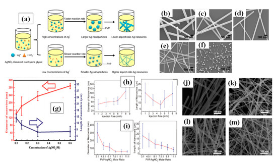
Figure 6.
(a) A schematic of the different concentrations of silver nitrate to change the AgNW diameter. The synthesis of AgNWs using different concentrations of silver nitrate; (b–f) PVP/silver nitrate molar ratios are (b) 2, (c) 4, (d) 8, (e) 16, and (f) 32, respectively. (adapted from [103] with permission from Elsevier, 2015) (g) Changes in nanowire diameter and length as a function of the AgNO3 concentration (adapted from [104] with permission from Royal Society of Chemistry, 2014). (h) Shows the Changes in nanowire diameter and length with different injection rate. (i) shows the changes in nanowire diameter and length with PVP:AgNO3 molar ratio. (adapted from [101] with permission from ACS publications, 2012) (j–m) FE-SEM images of AgNWs synthesized with PVP molecules of different chain lengths (j) PVP-55,000, (k) PVP-360,000, (l) PVP-1,300,000, and (m) PVP-1,300,000 + PVP-55,000 (a weight ratio of 1:1) (adapted from [105] with permission from ACS publications, 2012))
b. Metallic salts
Metal salts are of prime importance for the synthesis of longer nanowires. Various metallic salts have been used for scavenging the oxygen and electrostatic stabilization of Ag ions (Figure 5g,h). Zhang et al. synthesized ultralong nanowires of average length 220 μm and aspect ratio of 4000 times by optimizing the metallic salt (FeCl3) concentration as shown in Figure 7e–g [111]. They varied the FeCl3 concentration from 0 to 25 μm and found that 12.5 μm is the best concentration for synthesis. As the concentration decreased (<12.5 μm) the diameter of nanowire increased and on increasing the concentration (>12.5 μm) the nanowire length decreased. It has been reported that KBr can also be used as a conucleaent for one-step polyol method because of its good passivation property. Zhang et al. mentioned that KBr cannot grow the nanowires alone, but with NaCl/FeCl3 it can considerably help in reducing the nanowire diameter. They synthesized nanowires of sub 30 nm range with KBr assisted conucleation method [112]. The optimized ratio of NaCl:KBr (4:1) was used to synthesize ultralong nanowires with a diameter of 40 nm and an aspect ratio of about 2500; an SEM image of the synthesized nanowires is shown in Figure 7a,b [113]. They mentioned that Br− ions form smaller AgBr crystals than AgCl and passivates the 100 plane to help in diameter reduction. A schematic of this process is shown in Figure 7c. Cu ions are also used for the same contribution in synthesis. In order to investigate the correlation between copper ions concentration and nanowire dimension, Wang et al. demonstrated a rapid (30 min) synthesis polyol process at 160 °C. They demonstrated that an optimized CuCl2 concentration (0.36 mM) is necessary for longer nanowires Figure 7d [114].
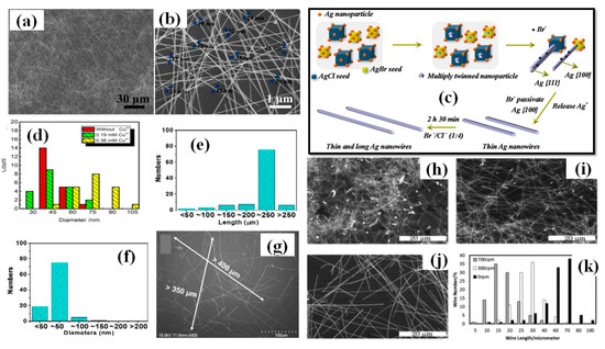
Figure 7.
(a) Low-magnification FE-SEM image of the synthesized AgNWs; and (b) representative high-magnification FE-SEM image of the synthesized AgNWs (c) A Schematic representation of the proposed formation mechanism of high aspect ratio AgNWs using Br-ions (adapted from [113] with permission from MDPI, 2019) (d) A statistical analysis diameter of AgNWs under different condition (adapted from [114] with permission from Elsevier, 2016).The distribution of (e) length, and (f) diameters in a count of 200 Ag NWs (g) SEM images of synthesized AgNWs (scale bar 100 µm) (adapted from [111] with permission from ACS publications, 2017). (h–j) The SEM images of AgNWs prepared at 130 °C with stirring speeds of (h) 700, (i) 300 and (j) 0 rpm (the inset photos have a scale bar of 30 μm. (k) Statistics of the length distribution of AgNWs with different stirring speeds (adapted from [117] with permission from Royal Society of Chemistry, 2013).
c. Temperature and time
The scientific measurement of temperature is attributed from average kinetic energy of the particles constrained in the system. One can conclude that temperature plays a crucial role for the interaction between the molecules as a little change in temperature can significantly change the results. Along with that it is well known that at high temperature ethylene glycol changes to glycolaldehyde, which can easily reduce Ag ions to pure Ag atoms [115]. Xia et al. used 160 °C temperature for 1 h in most of the AgNW synthesis. They mentioned that no nanowires were synthesized at 100 °C temperature while at higher temperature (>185 °C) only nanorods were formed. Unalan et al. reported a detailed study on temperature variation from 110 °C to 190 °C and found the optimum temperature is 170 °C [101]. Bergin et al. suggested that low temperature and longer synthesis time can enhance the length of nanowires with a vital difference while a quick synthesis leads to shorter but thinner nanowires [116]. Another report in support of the earlier hypothesis has been provided, where low temperature (130 °C) for longer time (12 h) leads the researcher to obtain nanowires of length 100 μm [117]. As the time is reduced (5 h) the nanowire length reduced to 65 μm at the same temperature
d. Stirring rate
The Ag nanowire synthesis using the polyol method is a one-pot process that does not require any external interception during the synthesis. Even oxygen present in the surrounding can affect the results, which is why most of the time the reaction is conducted in argon or nitrogen atomosphere. Researchers prefer autoclaves and oil baths to keep the reaction undisturbed from external influences [74,111,118,119]. As a proof of concept, Jiu et al. investigated the effect of stirring on nanowire synthesis. AgNWs of length upto 100 µm have been synthesized by adjusting the stirring speed (0–700 rpm) during the process [117]. The nanowires obtained without stirring were three times larger than those with stirring; an SEM image with histogram representation is shown in Figure 7h–k. It has been establish that higher stirring speeds may result in disturbing the reaction by transferring the oxygen molecule. The O2 molcecule results in oxidative etching that restricts decahedral twinned seed formation and promotes the formation of other nanostructures. Amirjani et al. studied the effect of stirring (0–2000 rpm) and recommended that high stirring rate results in low aspect ratio of nanowires and nanorods [120]. A slow stirring rate can be used to effectively reduce the AgNW from 200 nm to 130 nm. However, some studies have shown that increasing the stirring rate results in reducing both dimensions (diameter and length) of the nanowire [101].
3. AgNW Based Transparent Conductive Electrodes
Transparent conducting electrodes (TCEs) with high optical transmittance and low sheet resistance are crucial for development and performance of optoelectronic devices [128]. ITO is the most commonly used transparent conductive electrode (TCE) for various applications such as solar cells [129], flat panel displays [130], LED [131], OLED [132] and touch screen [133], because of its excellent optoelectronic properties [134] (transparency~90% and sheet resistance~10 Ω/sq). However, there are some major limitations of using ITO which include its brittle nature [135] and high fabrication costs [136]. The growth in demands of modern optoelectronic devices needs to fulfil many crucial characteristics such as solution based processing, low cost, scalable fabrication, excellent optical transparency, low sheet resistance, good mechanical (flexible, stretchable and stress consumable) properties and improved chemical stability [13,16]. Hence, these properties are critically important for application and evaluation of TCF performance using the Figure of merit (FoM). FoM depends on transmittance (T) and sheet resistance of the material. Transmittance follows lambert beers law and can be evaluated as
(where “a” is the absorption coefficient and “t” is the film thickness), while the sheet resistance can be simply calculated by keeping the electrodes at unit distance from each other such as the two or four probe method. The relation between T and can be written as:
where T is transmittance, Z0 is impedance of free space (377 Ω) and the ratio of and is known as (FoM), which determines the goodness of the fabricated TCF [137].
Researchers have proposed many alternatives to fulfil the above mentioned properties, such as graphene [138], CNT [139], AgNW [13] and (AZO) [140]. Graphene has high in plain conductivity with excellent optical transparency (~95) and low sheet resistance (50–1000 Ω) [141]. However solution processed graphene has high sheet resistance and chemical vapor deposition technique is too expensive for large scale applications due to the high temperature (>1000 °C) requirement [142]. CNT based transparent conducting electrodes are highly transparent (~90%), but the sheet resistance (200–1000 Ω) [139] of CNT is significantly higher as compared to ITO. Metallic nanostructures especially AgNWs (AgNWs) have arisen as a perfect alternative for transparent conducting electrodes due to their flexibility, low intrinsic resistance and excellent optical transmission [29]. The major requirement of transparency can be achieved by decreasing the density of the solution and minimizing the size of the material at the nanoscale [143]. Nanowires are the ideal material for such applications because of their crosslinking structure as they have two dimensions quantum mechanically confined to the nanoscale and one unconfined dimension that helps in conductivity and crosslinking to each other. Specific applications can be achieved by choosing a suitable nanowire size and diameter.
3.1. Transparent Conducting Electrode Fabrication Methods
In order to fabricate a AgNW solution based flexible transparent conducting electrodes (FTCE), diverse methods have been utilized such as spray coating [107,144,145], spin coating, drop casting, dip coating, vacuum filtration and transfer, roll to roll processing, mayer rod coating, doctor blade coating and printing. AgNW based FTCE are easy to fabricate and cost effective with high optical transmittance, high electrical conductivity and flexibility which makes it a probable contender for a range of future optoelectronic devices [31]. Finally a Table 2 has been inserted in the last of Section 3 to compare all TCE fabrication method along with variety of enhancement methods.
Table 2.
Summarized TCE fabrication and treatment method along with their comparison using FoM (Haacke’s formula).
3.1.1. Spray Coating
Spray coating is the simplest method of FTEC fabrication. It uses an airbrush or electrostatic sprayer with a very dilute concentration of AgNW solution for coating large areas on a variety of substrates [146,147]. There are many parameters that affect spray coating, e.g., flow rate, pressure of the nozzle, density of the solution sprayed, distance between substrate and nozzle along with the surrounding conditions such as temperature and humidity. Madaria et al. utilized a spray coating technique to obtain transparent conductive AgNW films on random substrates with high uniformity. The optical transparency and sheet resistance of the films could be optimized by varying the density of the AgNWs in the spraying solution. Using a polydimethylsiloxane (PDMS) assisted contact transfer technique, they transfer the AgNW network to PET substrates to fabricate a flexible TCE with an optical transparency of 85% and sheet resistance of 33 Ω/sq [148]. The biggest challenges for fabricating flexible TCE is to transfer the electrode to dissimilar arbitrary substrates because of the risk of cracking and damaging [146,149]. Consequently, a transparent conducting AgNW–polydimethylsiloxane (PDMS) electrode fabrication and transfer technique by water-assisted transfer printing method was reported as shown in Figure 8h [149]. This advanced method displays a strong capability for transferring the AgNW film on various hydrophilic substrates without any significant change in the characteristics of the film as depicted in Figure 8i. A high ratio of DC conductivity () to optical conductivity () with 82% transmittance, 9 Ω/sq sheet resistance, tensile strain (0 to 50%), and 2 mm bending radius flexibility was obtained without significant loss of conductivity. Choi and coworkers demonstrated a two-step spray-coating method for fabrication of AgNW–PEDOT:PSS composite based flexible electrode as shown in Figure 8a–e. The first step involves spray coating AgNW and later PEDOT:PSS is spray coated on predeposited AgNW to attain 84.3% transmittance and 10.76 Ω/sq sheet resistance [144]. The PEDOT:PSS significantly enhances the stability under compression and bending, reduces the junction resistance and surface roughness as shown in Figure 8f,g.
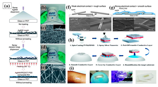
Figure 8.
(a) Schematic diagram of the fabrication of AgNW–PEDOT:PSS composite electrodes through successive spray coatings. (b) AgNW mesh deposited on a flexible PET substrate by spray coating and its SEM image. (c) The inset image shows the cross-sectional view of the AgNW network. (d) AgNW–PEDOT:PSS composite film on a PET substrate with 81.7% (at 550 nm) of transmittance and 11.3 Ω/sq of sheet resistance. (e) SEM image of the AgNW–PEDOT:PSS composite film and a cross-sectional inset image. SEM image of AgNW film before (f) and after (g) PEDOT:PSS spray coating. (adapted from [144] with permission from Royal Society of Chemistry, 2013)Schematic of the Water Transfer technique process for AgNW TCEs. (h) (1) A prefabricated sacrificial layer (PVP) and a flexible framework (PDMS); (2) spraying of AgNWs on the top of PDMS after plasma treatment; (3) peel off the fabricated PVP-PDMS and AgNW film (4–5) transferred nanowire devices on a prehumidification target substrate with a sacrificial layer in between. (6) final film on random substrate (i) The corresponding photographs of various nonconventional substrates, including skin, a balloon, a round-bottomed flask, and an elastomeric textile (adapted from [149] with permission from Royal Society of Chemistry, 2019)
The correlation between T and Rs can be evaluated by percolative FoM and the percolation exponent [150]. The percolative FoM depends on nanowire properties, while the percolation exponent depends on the properties of the network. Hence, two strategies can be implemented in order to enhance the output of TCEs. The former consists of enhancing the nanowire dimensions (high aspect ratio), and the latter of improving the network properties (low junction resistance and higher stability). Scardaci et al. tried to improve the network properties by optimizing the percolation exponent and found that nozzle pressure is the critical parameter that effect the size of the droplets, network uniformity and the morphology of the fabricated film [151]. They fabricated a TCE with 90% transmittance and 50 Ω/sq sheet resistance by varying the nozzle pressure while a maximum 94% transparency was achieved at higher sheet resistance. In 2020, another group of researchers tried to enhance the percolative FoM by refining the dimensions of nanowires (average length 130 µm, aspect ratio > 1000) and the synthesized AgNWs were spray coated on a glass substrate to obtain a TCE of 91% transmittance and 4.6 Ω/sq sheet resistance [122].
3.1.2. Spin Coating
Spin coating is considered as the most common and simple way for AgNW based FTCE fabrication [152,153,154,155]. During spin coating, a low concentration of AgNW solution is dropped on the substrate that is spun by the spin coater under a high centrifugal force, resulting in the solution being uniformly distributed over the substrate. There are different parameters that affect the properties of the fabricated TCE such as spinning rate, concentration of the solution and the time duration of coating. Leem and coworkers used an oxygen plasma pretreated glass substrate to optimize spin coating parameters by varying the spinning rate in the range 1000–5000 rpm. Nanowires with a length of several tens of micrometers were used and they found that the transmittance of the film decreased significantly when the spinning rate decreased from 5000 rpm (98% transmittance with 36 Ω/sq sheet resistance) to 1000 rpm (89% transmittance with 10 Ω/sq sheet resistance), which can be seen in Figure 9e below [153].
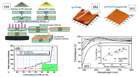
Figure 9.
(a) A schematic procedure for AgNW/ PVA thin film fabrication by spin coating, (b–c) surface morphology of (b) bare AgNW and (c) AgNW/PVA composite film on PET (d) Transmission-resistance graph for AgNW and AgNW/PVA composite electrodes (adapted from [156] with permission from Royal Society of Chemistry, 2014) (e) a transmittance vs. resistance graph for different spin coating speed (1000–5000 rpm) (adapted from [153] with permission from John and Wiley sons, 2011).
Apart from the mentioned parameters, the nanowire dimensions such as very thin diameter (~20 nm) and high aspect ratio (>1000) are the two most notable characteristics to enhance percolative FoMs. Selective precipitation method was used for nanowire purification to enhance the transparency by 2% and finally a TCE with 97.5% transmittance and 70 Ω/sq sheet resistance was fabricated by spin coating followed by thermal annealing [155]. AgNW based conducting films have non-uniformity and high surface roughness due to random alignment and junctions between nanowires. A composite PVA-AgNW film of 86.9% transmittance and 0.75 Ω/sq sheet resistance was fabricated to improve the mentioned properties as shown in AFM image of bare and composite film in Figure 9b–c [156]. Two separate PET substrates were used to fabricate AgNW and PVA film. Consequently, the fabricated AgNW film was positioned on the PVA film to completely cover the AgNW network using mechanical pressure; a schematic describing the procedure for film fabrication is shown in Figure 9a, and a transmission-resistance graph is presented in Figure 9d. AgNWs have been known to suffer from oxidation when exposed to chemicals or air. It has been reported that amorphous aluminium doped zinc oxide (a-AZO) has a highly compact structure, which can effectively guard the AgNW network to enhance the chemical stability as an anti-oxidative shield. An optimized three layered a-AZO/AgNW/ AZO composite electrode was fabricated using spin coating with a 88.6% transmittance and 11.86 Ω/sq sheet resistance [157].
3.1.3. Drop Casting
Drop casting comprises of dropping a dilute AgNW dispersed solution on a transparent substrate. Usually a surface treatment of the substrate is required before drop casting to ensure that the solution evenly spreads on the substrate surface [158,159]. If pretreatment is not performed, there are higher chances of nonuniform distribution of the AgNWs on the surface, resulting in increased surface roughness.
Generally, a thermal treatment is preferred after the solution is drop casted on surface to remove the dispersant and enable annealing of the AgNW network. The AgNW solution concentration and volume of the dropped solution are two important factors that must be optimized to fabricate a good transparent electrode using drop casting. A flexible TCE made of poly-acrylate (PA) AgNW composite with high transparency and low sheet resistance comparable to flexible ITO electrodes was fabricated using drop casting as shown in Figure 10a followed by curing with UV light to enhance the electrode properties [160]. Cheng et al. synthesized AgNWs with great aspect ratio via a novel polyol method without the use of halides ions [161]. The as-prepared AgNWs were drop casted on a patterned glass substrate to form a uniform conductive network. After drying, liquid polydimethylsiloxane (PDMS) was poured on the AgNW network layer followed by curing and peeling off the AgNW/PDMS film. This stretchable electrode displayed good optoelectronic characteristics with a sheet resistance of 14 Ω/sq and a transmittance of 90% without any post treatment as shown in Figure 10c,d. A schematic of the fabrication procedure been shown in Figure 10b. In 2019, Chen and coworkers demonstrated a modified drop casting method to fabricate AgNW-PDMS composite based flexible transparent conducting film, which fulfils some of the key requirements of modern optoelectronics [162]. The AgNW network was drop casted on the PDMS substrate to create the required pattern with the help of a stencil mask. The PDMS substrate was pretreated with oxygen plasma to enhance the adhesive properties between the AgNW and the substrate. The conductive polymer film displayed good optoelectronic properties with a 15 Ω/sq sheet resistance, 85% transmittance, a relatively uniform surface with surface roughness of about ∼22 nm along with 70% stretchability, and 70% bending which have been shown in Figure 10e–g. It is worth mentioning that drop-casting technique is not highly scalable and the process is not completely repeatable each time.
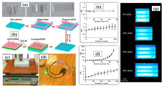
Figure 10.
(a) illustrating the shape memory property of an AgNW/polymer electrode: photographs of a highly curved AgNW/polymer electrode (left) and its steady relaxation at 120 °C to an intermediate (center) and recovered shape after some time (right). (adapted from [160] with permission from John and Wiley sons, 2011) (b) A schematic procedure for AgNW/PDMS electrode fabrication by drop casting, (c) sheet resistance of the transparent electrodes (T = 81%) measured using a four-point probe instrument; (d) flexible transparent conductive film (T = 90%) in an electrical circuit powering three LEDs. (adapted from [161] with permission from Royal Society of Chemistry, 2014))∆R/R versus (e) bending strain and (f) stretching strain of fabricated electrode (g) real time device testing with no decay up to 60% stretching (adapted from [162] with permission from ACS publications, 2019).
3.1.4. Vacuum Filtration and Transfer
The vacuum filtration method is quite popular for its usability for transferring AgNWs on a variety of substrates including polymer films [163,164,165,166,167,168]. The process includes pouring or dropping a dilute AgNW solution on a filter paper supported by a vacuum filtration. The filter paper helps in constructing the nanowires network uniformly by filtering out the solvent and nanocrystals. Consequently, high quality nanowires network can be obtained on the filter paper, which can then be transferred to another substrate. The filter paper pore size, vacuum pressure and AgNW solution concentration [168] are the parameters of prime importance. Wu et al. for the first time introduced 1-dimentional nanostructured thin film fabrication using vacuum filtration and transfer [163]. Though the aspect ratio of AgNWs was quite low (~76.4), transmittance of 92% and 1 Ω/sq sheet resistance could be achieved. Lee et al. synthesized ultralong nanowires of length up to 500 µm using a successive multiple growth (SMG) method. They fabricated TCEs with a 89–95% transmittance and sheet resistance 9–69 Ω/sq by using vacuum filtration [164]. Hong and coworkers gave a novel idea of using cellulose nanofiber paper that acts as a filter as well as substrate [166]. A schematic of the method with fabricated TCEs is shown in Figure 11a,g as the process avoided the AgNW network transfer to another substrate, a relatively lower 12 Ω/sq sheet resistance with 88% transmittance was observed as compared to other conventional methods shown in Figure 11b. The ‘filtration coating’ offers homogeneity on the surface and low AgNW junction resistance which can be seen in Figure 11c–f. Surface homogeneity was attained as the nanowires are embedded in the pores of the nanofiber paper during the vacuum filtration process. Conventional methods such as spin coating, spray coating and drop casting suffer from the coffee-ring effect since these methods generally use annealing for drying process, which promotes the nanowire agglomeration at specific areas and results in a nonhomogeneous distribution. As the AgNW network shows effective bonding by rooting inside nanofiber paper, it enables good flexibility of the transparent conducting film with negligible changes in the electrical conductivity. Recently, Won et al. introduced a novel and effective fabrication method for patterning a TCE into various shapes by introducing the Kirigami approach for highly flexible and stretchable E-skin applications. These Kirigami patterned electrodes possess ultrastrechability for a range up to 400%, with strain-invariant electrical properties for more than 10,000 cycles [119]. A dilute AgNWs solution was used to transfer the AgNW network onto a glass substrate by vacuum filtration. Next, colorless polyamide (cPI) was spin coated followed by curing (to enhance the adhesion between AgNW and cPI) and peeling off. The fabricated FTCE on cPI substrate exhibited a transmittance of 95% and a sheet resistance of 50 Ω/sq with excellent flexibility and stretchability. The results of a 0 to 400% stretchability test for 10,000 cycles are shown in Figure 11h.
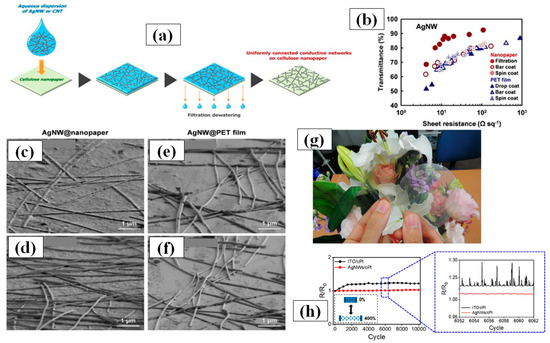
Figure 11.
(a) Putative process of the formation of AgNW on nanopaper by drop and filtration coating, (b) A comparison between of optoelectronic properties of fabricated TCE between various methods. AgNW@nanopapers prepared by (c) filtration coatin and (d) bar coating and AgNW@PET films prepared by (e) drop coating and (f) bar coating (g) Optical images of original nanopaper (left), CNT@nanopaper (middle) and AgNW@nanopaper (right). Paper size: 75 mm in diameter. (adapted from [166] with permission from Springer Nature, 2014) (h) R/R0 vs no. of cycles with 0 to 400% strain each time of ITO/cPI and AgNW/cPI (adapted from [118] with permission from ACS publications, 2019).
It should be noted that the vacuum filtration method works efficiently for nanocrystals of size higher than the micrometer range. However, while dealing with size dimensions in the nanometer range, the loss of material in the filtrate can be significant and this loss is enhanced during subsequent transfer to another substrate.
3.1.5. Doctor Blade Coating
Doctor blade coating is a simple process that uses a well-dispersed and homogenous nanomaterial ink with suitable solvent, binder and dispersants [169,170,171]. The film thickness depends on the distance between the blade and substrate, while the surface morphology depends on the density of ink and blade speed [172]. Krantz et al. in 2011 reported on AgNW solution processed electrodes as a substitute for ITO for organic solar cell application [170]. AgNWs were deposited on a glass substrate to fabricate transparent conducting electrodes with high transmittance, i.e., 90%, and low sheet resistance, i.e., 9 Ω/sq, by using doctor blade coating at moderate temperatures. Zhang et al. introduced a solution processed multilayer fabrication of sandwiched rGO/AgNWs/rGO TCE on PET and glass at low temperature (~50 °C) [173]. The rGO sheet aids in enhancing electrical contact of AgNWs by connecting detached nanowires and reduces the overall surface roughness. The fabricated film exhibited high transmittance, low sheet resistance and high stability due to presence of rGO as an antioxidative shield. The same research group presented another multilayer film structure consisting of AgNW-poly vinyl butyral (PVB) and aluminum doped ZnO nanoparticles (AZO) using doctor blade coating method and attained a very low sheet resistance with a transmittance of over 94%. The PVB layer effectively improves the adhesion property between the glass and film while the AZO NPs enhance the thermal stability and reduce the sheet resistance [174]. Hwang and group introduced a novel material, UV-curable Raygloss, which can be used as a coating layer as shown schematically in Figure 12a. This layer does not significantly affect the optoelectronic properties of the film but considerably enhances the mechanical properties against scratches (100 times shown in Figure 12b), wipes (60 times, shown in Figure 12c), bending (300,000 times) and stability against oxygen [174]. Interestingly, a small increase in optical transparency from ~87.7% to ~88.3% was observed due to the presence of this coating layer. This observation can be explained by Fresnel’s theory of reflection, which states that light reflection at a specific surface can be reduced by introducing a coating layer which has a refractive index value (Raygloss = 1.54) between that of the rarer (air = 1) and denser medium (PET = 1.64) [175].

Figure 12.
(a) Illustrations of the patterning process of Raygloss®/Ag nanowire electrodes. (b) Change in optical transmittance, haze, and sheet resistance as a function of the number of scratches for the bare Ag nanowire electrodes and Raygloss®/Ag nanowire electrodes, (c) The wiping test results of the bare Ag nanowire electrodes and Raygloss®/Ag nanowire electrodes (adapted from [174] with permission from Elsevier, 2017). Photographs of a large-area (18 cm × 9 cm) and flexible Ag NW TCE (d) before and (e) after bending by 180°. Red dashed lines highlight the edges of the flexible Ag NW TCE (adapted from [176] with permission from Royal Society of Chemistry, 2020).
A highly transparent multilayer structure for a solar cell device embedded with both electron and hole collecting AgNW electrodes was reported by using the doctor blade technique [169]. In 2020, Huang et al. fabricated a polymer based ultraflexible AgNW transparent conducting film on glass and PET substrate. The fabricated TCF properties were optimized by changing the concentration of the AgNWs solution and the height of the blade. The coating speed is considered as a vital parameter for uniform surface coating and. they found that a nonhomogeneous coating of AgNW was observed when the coating speed was less than 50 mm/s. Subsequently, a transparent polymer layer was coated on the AgNW network followed by curing and peeling off from the glass substrate. The polymer film with good optoelectronic properties was highly flexible and could be bent up to 180° without any change in resistance and shows potential for applicability in next-generation flexible and foldable optoelectronic devices [176]. A picture of flat and 180° folded transparent electrode is shown in Figure 12d,e.
3.1.6. Mayer Rod Coating
Mayer rod coating, unlike other solution-processed techniques, is considered as a more scalable [177], accurate and faster method for deposition of nanowires to make a thin film for practical applications. The Mayer-rod consist of a solid bar with helical metal wires wound on it. The ink density, surface of substrate, meniscus height (distance between the substrate and rod) and slit size are the key parameters for Mayer rod coating. Slit size of Mayer rod depends upon the density of wire looping and it can be varied accordingly with application requirements (51–381 μm as shown in Figure 13a) [178]. The process involves positioning the AgNW solution/ink on one side of substrate and then uniformly spreading the solution on the substrate using the Mayer rod [179,180,181]. Hu et al. first fabricated a TCE of 80% transmittance and 20 Ω/sq sheet resistance by Mayer rod coating and later researchers improved the efficiency of the method using minor modifications [182]. A simple and efficient Mayer rod coating method was used for fabrication of highly cross-aligned AgNW transparent electrodes with good optoelectronic properties (21 Ω/sq sheet resistance at 95.0% transmittance) on a large surface area (20 × 20 cm2), while the randomly aligned AgNW network provided 90.4% optical transmittance and 21 Ω/sq sheet resistance [180]. An optical image of the aligned nanowires can be seen in Figure 13c,d. The meniscus height and slit size optimization is important as the alig nment pattern of nanowires majorly depends upon the shear force, which further depends on the height of the deposited meniscus film. As shown in Figure 13e, a strong shear force is obtained with a thin meniscus film which helps to align the AgNW in a unidirectional manner. A thick meniscus film suffers from misalig nment due to weak shear force near the substrate surface. A schematic for the procedure is shown in Figure 13b. Yang et al. fabricated an AgNW-PEDOT: PSS composite TCE with a sheet resistance of 12 Ω/sq, transmittance of 96% and a uniform surface with only 7.13 nm surface roughness [183]. The PEDOT: PSS nanosheets aid in welding the nanowire junction to reduce the junction resistance from 32 Ω/sq to 12 Ω/sq and improve the adhesion between AgNWs and the substrate. A SEM image of AgNW-PEDOT:PSS film is shown in Figure 13h. The fabricated TCE was used as the top and bottom electrode for developing highly sensitive and flexible touch panels of 7 × 7 cm2 area, which is highly stable against wiping (500 times), bending (5000 times) and writing (2000 times). In 2020, an optimized and quick synthesis of ultralong AgNWs have suggested that Mayer rod coating delivers improved outcomes than spray coating with a significant difference of 3% in transparency (rod coating = 94% and spray = 91%) for same sheet resistance of 5 Ω/sq [122]. The reason for the difference in the results were essentially because of alig nment factor as the rod coated TCE had more aligned nanowires while the spray coated TCE had more curved nanowires as shown in Figure 13f,g. The AgNW based TCE provides an additional advantage of high transparency in NIR region (94%), while the transparency for NIR region decreases to 35% in case of ITO as shown in Figure 13i [184]. Some modern applications demand transparency in the NIR region and AgNW based TCEs show promise for these applications. The change in transparency over a wide wavelength range (λ = 0–2500 nm) for AgNW based thin films was quite small.
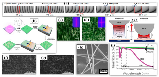
Figure 13.
(a) Schematic illustration of the specifications of various Mayer rods. The rod number determines the diameter of wrapped wires and the open area. (b) A Schematic of procedure for the solution-processed bar-coating assembly to fabricate unidirectional and cross-aligned AgNW arrays. Before the bar-coating assembly, PLL solution is coated on O2 plasma-treated target substrate to form amine groups on the surface. Consecutively, the meniscus dragging produces highly aligned AgNW arrays. The cross-aligned AgNW array is formed by repeating the bar-coating assembly in a perpendicular direction to that of the pre-aligned AgNW arrays. Fast Fourier transform (FFT) analyses of the optical micrographs, indicating the direction and uniformity of the aligned AgNW structures. (c) Unidirectionally aligned and (d) cross aligned AgNW arrays. The scale bars are 40 μm. (e) Schematic showing the intensity distribution of shear force according to the variation of the height (δ) of meniscus (adapted from [180] with permission from ACS publications, 2017). SEM images of the AgNW networks deposited by (f) Mayer rod coating and (g) spray coating. Rsh is the sheet resistance while the stated transmittance (T) is at 550 nm and relative to the transmittance of the bare glass (adapted from [122] with permission from Royal Society of Chemistry, 2020). (h) SEM image of AgNW bound by PEDOT:PSS, the illustration shows the high uniformity and continuous of the fabricated composite FTCE (adapted from [183] with permission from Royal Society of Chemistry, 2019) (i) Transmittance vs. wavelength for AgNW networks at nanowire diameters of 30 nm, 70 nm, 100 nm, and 120 nm. The transmittance of AgNW networks are much greater in the near-infrared region than commonly used indium tin oxide (adapted from [184] with permission from Royal Society of Chemistry, 2020).
3.1.7. Roll-to-Roll Slot Die Coating
Roll-to-roll slot die coating is a simple technique for large-scale film deposition on a substrate. The major advantage associated with this method is the large area surface uniformity in a controlled manner with film thickness ranging from the nanometer to micrometer range. Some vital parameters for roll-to-roll processing include ink feeding rate, coated-web gap and web speed. An optimized combination of these parameters can be used to fabricate TCE with high FoM. In order to make easy understanding of forthcoming parameters Figure 14a has been inserted. An increase in the web speed results in thinner coating layer with less density of conducting material which in turn increases the sheet resistance and transmittance [185]. Furthermore, research has shown that silver inks demonstrate better optoelectronic properties as compared to conductive polymer inks. Linda et al. used similar roll-to-roll parameters (web gab = 40 µm, pump rate = 145%, and web speed = 2.4 m/min) and found that the conductive polymer had 100 Ω/sq sheet resistance at 80% transmittance while the AgNW ink had 40 Ω/sq sheet resistance at the same transmittance [186]. An optimized one-step AgNW/ PEDOT:PSS ink based TCE using roll-to-roll slot die coating has also been demonstrated as shown in Figure 14b. AgNW/ PEDOT:PSS was deposited at 2.7 m min−1 of ink feeding rate and a static 100 µm shim gap on a large surface area (46 cm × 20 m) PET substrate with good optoelectronic properties (sheet resistance ~75 Ω/sq and transmittance > 90%) [187]. A picture of the fabricated film is shown in Figure 14d. Jeong et al. suggested that calendaring is an impactful process in order to improve the efficiency of roll-to-roll slot die coating method [188]. A combination of roll-to-roll slot die coating and calendaring process machine is shown in Figure 14c which can control roll temperature, pressure and web speed to provide low sheet resistance (28 Ω/sq) with good transmittance (86%). The calendaring process parameters (pressure and temperature) significantly improves the contact between Ag nanowires by eliminating the PVP surfactant coating to reduce the sheet resistance and surface roughness as seen in Figure 14e,f. Kim and coworkers introduced an AgNW network based TCE fabrication on PET substrate using roll-to-roll slot die coating and they achieved varying transmittance (89–90%), haze (0.5–1%) and sheet resistance (30–70 Ω/sq) by optimizing the flow rate of shear thinning silver ink in die slot. The final application as a touch screen has 90% optical transmittance and sheet resistance of 50 Ω/sq [189].
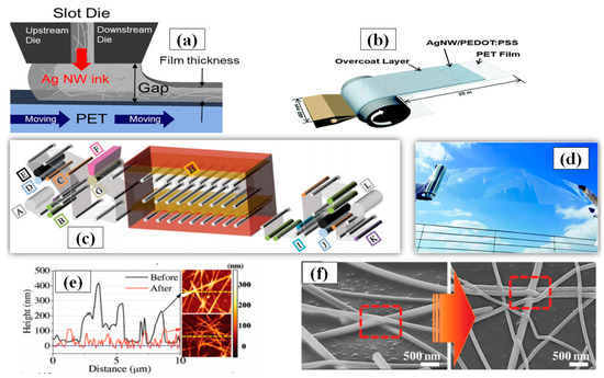
Figure 14.
(a) schematic structure of a slot die head used for Ag NW coating with the influencing parameters (adapted from [188] with permission from John and Wiley sons, 2018) (b) A Schematic diagram of slot-die roll-coating process and structure of the AgNW/PEDOT:PSS conducting film (adapted from [187] with permission from Royal Society of Chemistry, 2015) (c) Roll to Roll slot-die coating of AgNWs: (a) schematic of R2R slot-die coating with calendaring process machine (A: unwinder, B: edge position controller, C: load cell, D: infeeder, E: nip roll, F: slot-die, G: backup roll, H: far-infrared dryer, I: accumulator, J: outfeeder, K: dancer, L: rewinder (adapted from [189] with permission from Springer nature, 2016) (d) Photographic image of the AgNW/PEDOT:PSS conducting roll film fabricated in this study (adapted from [187] with permission from Royal Society of Chemistry, 2015) (e) AFM data before and after calendaring (f) SEM image of AgNWs before and after calendering process. (adapted from [189] with permission from Springer nature, 2016).
3.1.8. Dip-Coating
Dip-coating is a very simple method of dipping the substrate in a solution containing the nanomaterial to be coated. After dip-coating, the substrate is removed from the solution followed by a drying process. During the drying/annealing process, the nanowires stay on the surface while the solvent is evaporated. Solution concentration, withdrawing speed of the substrate and atmospheric drying conditions (temperature and pressure) are critical parameters, which must be optimized in order to attain good optoelectronic properties of the TCE [190]. The dipping direction of the substrate can be changed to reduce the sheet resistance and increase the number of nanowire junctions [191]. Ackermann et al. reported a low haze and ultra-TCE with a sheet resistance less than 100 Ω/sq by simply optimizing the concentration of the AgNW, the substrate dipping direction and withdrawing speed [192]. The improved optoelectronic performance can be seen from the transmittance vs. resistance graph as shown in Figure 15a. In order to further enhance the optoelectronic properties, a two-step dip coating method on PET substrates can also be used [193], as demonstrated in Figure 15b,c. The flexible PET film was dipped into the AgNW solution (0.1 mg/mL) and withdrawn at a speed of 1 cm s−1 with the help of a programmed machine. In the second step, the substrate was rotated by 90° and dipped to enhance the number of nanowire junctions and improve conductivity. The two step dip-coating resulted in a fabricated TCE with improved optoelectronic properties (T = 92% and Rs = 35 Ω/sq). Similarly a simple method of homogeneous AgNW network electrode on glass has been fabricated by recognizing suitable processing constraints such as dipping cycles (between 10 and 150 cycles) and withdrawing speeds (0.2–2.5 mm/s) [194]. A further treatment of annealing and PEDOT:PSS coating is used to reduce the surface roughness and obtain 85% transmittance and 15 Ω/sq sheet resistance. Ahn et al. presented a detailed discussion on optoelectronic properties of AgNW thin film using dip coating for mass production [195]. A quality correlation between the nanowire parameters such as nanowire length, diameter and aspect ratio has been explained.
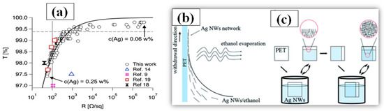
Figure 15.
(a) The optical transmission T versus the sheet resistance Rs. (adapted from [192] with permission from Springer nature, 2016) (b) Schematic illustration of nanowire assembly in the dip-coating process. (c) Two-step dip-coating process after rotating the substrate in perpendicular direction (adapted from [193] with permission from Royal Society of Chemistry, 2015)
3.1.9. Printing Techniques
Printing techniques such as inkjet printing [196,197], gravure printing, screen printing, electro-hydrodynamic jet (EHD) printing and capillary printing have been widely studied, as these techniques enable the printing of flexible and stretchable electrodes. In order to attain a TCE with a high figure of merit, the selection of ink dispersant and concentration of the AgNW must be optimized to obtain a suitable ink. Printing techniques have been widely utilized for large scale production of TCEs, but the minimum achievable resolutions are still in the low micrometer range. It is worth mentioning that substrate and ink interaction, printing speed and ink pressure play a vital role in effecting the quality and printing accuracy of the ink.
Lu et al. used an inkjet printing technique to fabricate the upper electrode of a semi-transparent organic photovoltaic (OPV) device with a power efficiency of 2.71% [196]. They observed that printing the ink in successive steps could immensely enhance the conductivity while resulting in a slight decrease in transparency of the electrodes. Li et al. used a screen printing technique to fabricate flexible and stretchable TCE with a transmittance of 73% and sheet resistance less than 2 Ω/sq [198]. A high FoM (135) with good stability after 1000 bending and stretching cycles was achieved by optimizing the printing parameters, ink formulation and laser post treatment. Recently, a AgNW/GO hybrid TCE with enhanced optoelectronic properties was fabricated using screen printing and showed feasibility for long-term electrocardiography monitoring. The AgNW dispersion was printed on a PET surface followed by coating of a GO layer to avoid oxidation [199]. Gravure printing involves the use of an engraved cylinder which is fixed to a rotary printing press and has been commonly used for commercial printing of magazines and newspapers, [5,200]. The importance and relation between ink pressure, speed and rheological behavior of AgNW ink during gravure printing has been reported [201]. Gravure printing has been implemented to fabricate a AgNW based TCE on PET substrate with 95% transmittance and 32 Ω/sq sheet resistance. In order to attain accuracy and control over percolative FoM and the percolation exponent, capillary printing techniques have also been introduced [202]. It was observed that the partial alignment of AgNWs during capillary printing shows better optoelectronic properties as compared to randomly aligned AgNWs. Furthermore, the luminance efficiency of the fabricated polymer light-emitting diodes (PLEDs) increased by 30% for partially aligned AgNWs. In addition, a polymer solar cell (PSC) with a power efficiency of 8.57% was also fabricated, which is one of the highest reported values obtained using AgNW based TCE. All the above mentioned printing techniques are still limited in terms of the minimum achievable resolution [203]. It is also worth mentioning that EHD printing was shown to be able to approach a higher resolution and accuracy as compared to other techniques [204]. A detailed study to fabricate flexible TCE and Ag grids of different line width and line gap has been demonstrated using EHD printing [205]. Park et al. used a modified electro-aerodynamic jet printing technique to implement an aerosol deposition method in order to enhance the optoelectronic properties of the fabricated Ag grid [206]. Ag nanoparticles were electrically charged and sprayed under application of a high AC voltage (7 kV) on a prepatterned Ag grid based PET substrate. Consequently, a reduction in sheet resistance from 7.38 Ω/sq to 1.95 Ω/sq was observed at 84% transmittance. Cui et al. reported AgNW based EHD printing techniques for large area substrates and demonstrated a dependence of ink viscosity, AgNW concentration and blade moving speed on the final results obtained on a variety of substrates such as PDMS, PET, Paper and glass [207]. We anticipate that the performance of these printing techniques will continue to improve in the future and enable large scale industrial TCE manufacturing for a wide range of optoelectronics devices.
3.2. TCE Enhancement Method
A range of treatment methods have been utilized to reduce the contact resistance (Rc) at the nanowire-nanowire overlapping junction and improve the optoelectronic properties of the solution processed TCE. The polyol method, which is the most commonly used method for large-scale synthesis of AgNWs, generally uses PVP as a surfactant to avoid agglomeration between AgNWs. For e.g., a 50 nm PVP coating as shown in Figure 16a can result in high junction resistance and pretreatment is required to reduce the thickness of the PVP layer as shown in Figure 16b,c. A range of pre and post fabrication treatment methods such as solvent washing, mechanical pressing, joule heating, thermal annealing, plasmonic welding, polymerization and electro-deposition have been used by researchers to improve the final optoelectronic properties of the TCE as discussed in further detail in the following sections.
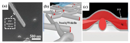
Figure 16.
(a) SEM images of AgNWs surrounded by PVP layer of ~50 nm thickness (b,c) the concept of treatment for sheet resistance reduction (adapted from [188] with permission from John and Wiley sons, 2018).
3.2.1. Solvent Washing
Solvent washing, also known as centrifugation technique, is a widely used pretreatment method after AgNW synthesis to separate out organic and inorganic contaminants. In a solution based AgNW TCE, the value of the sheet resistance (RS) primarily depends on the nanowire contact resistance (Rc). The PVP encapsulating layer insulates the transmission of electrons at the nanowire junction by quantum tunneling effects as shown in Figure 17a. Consequently, the PVP layer, which can act as a tunneling barrier, can be removed or its thickness can be reduced to decrease the Rc as well as the sheet resistance (RS). It has been demonstrated that with multiple washing process with water there is a significant reduction in Rc (Figure 17b). As a proof of the concept, TEM images of AgNW without washing and after washing for 20 times have been shown in Figure 17c [208]. A significant reduction in the thickness of the PVP layer by about 75% was observed after the washing step. Furthermore, two transparent conducting electrodes were fabricated using Mayer rod to investigate the difference in optoelectronic properties. Improvement in transmittance and reduction in haze were seen after multiple washing steps, as shown in Figure 17d. The removal of PVP layer using a post-treatment method after TCE fabrication typically restricts the final application of the device due to substrate susceptibility toward various parameters such as solvent used and treatment time. Wang et al. performed a pretreatment of AgNW by solvent washing (ethanol) and observed a significant decrease in PVP layer thickness from 13.19 nm to 0.96 nm after four solvent washing steps [209]. A dramatic decrease in sheet resistance from 5 × 10⁴ Ω/sq to 93 Ω/sq at 95% transmittance was observed after the washing steps. Lee and coworkers used methanol to remove the PVP layer to efficiently enhance the nanowire junction conductivity by reducing the PVP layer thickness from 4 nm to 0.5 nm using 5 successive washing cycles [210].
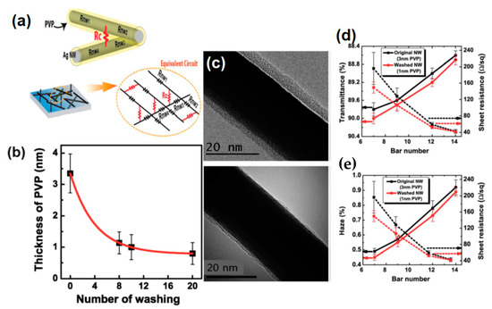
Figure 17.
(a) Conceptual illustration of contact resistance and nanowire resistance, and the equivalent circuit of AgNW network which can be used for Monte Carlo simulation. (b) Average thickness measured for the PVP capping layer on the AgNWs with different numbers of repetitions of the washing process. (c)TEM image of an as-synthesized PVP-capped AgNW and the same NW after washing 20 times with DI water. (d) Transmittance versus bar number of a Mayer rod with error bars (e) Haze versus bar number of a Mayer rod with error bars (the values of RS of the corresponding samples are plotted together in order to indicate the different areal coverage of the AgNW networks that were coated with different bar numbers of the Mayer rod). (adapted from [208] with permission from Royal Society of Chemistry, 2016)
3.2.2. Thermal Annealing
Thermal annealing has been widely used as a post treatment method for AgNW based TCEs due to its simplicity, feasibility and efficiency at large scale [106,153,164,211,212]. The temperature annealing process can be implemented in two ways, which include low temperature annealing (<150 °C) for longer time and high temperature (~200 °C) annealing for shorter time depending upon the nanowire and substrate stability. Zhang et al. fabricated a highly stable and uniform TCF using silver ink dispersed in ethanol via Mayer rod coating [213]. Various post treatment methods such as natural drying, static heating and dynamic heating (as shown in Figure 18a–c, respectively) were used to investigate the optoelectronic properties and surface morphology. Sheet resistance of 24 Ω/sq and 91% transmittance with excellent surface uniformity over a large area (20 × 40 cm) were accomplished in case of dynamic heating (UF = 0.2915) treatment as compared to natural drying (UF = 0.5167) and static heating (UF = 0.3415). Based on the PVP layer coating, it is important to choose an optimized temperature for annealing. Thermal analysis of PVP indicates that the glass transition temperature (174 °C) and melting point (224 °C) are quite high and the substrate material can be susceptible at these temperatures. Air dried AgNW TCE was annealed at 200 °C and this resulted in slight melting of the PVP, which aids in nanowire fusion [214]. An SEM image of the melted PVP and nanowire fusion is shown in Figure 18d,e. A detailed model on the evolution of AgNW sheet resistance (reduction, stabilization and spheroidisation of AgNWs which can be seen in Figure 18f–j) by thermal annealing has been reported [215]. A TCE of 90% transmittance and 9.5 Ω/sq of Rs was fabricated by optimizing the annealing conditions. Four possible mechanisms for resistance variation with temperature which include Rayleigh instability of the AgNW diameter, organic residue desorption, PVP degradation and sintering have been mentioned. Later, the same group proposed a method to investigate the optoelectronic properties of AgNW based TCE by optimizing nanowire density, dimensions and thermal annealing procedure [216]. They proposed that thermal stability is dependent on the nanowire size dimensions and suitable selection of all three parameters results in highest reported FoM with T = 89.2% and Rs of 2.9 Ω/sq. For organic applications, humidity assisted annealing is a better approach, which requires a low temperature for Rs reduction. The humidity absorption at the surface of PVP reduces the glass transition temperature by softening it, which enables annealing to be performed at a lower temperature of 60 °C [217]. The method is quite efficient as annealing at 60 °C provides the same results with conventionally annealed TCEs at ~200 °C.
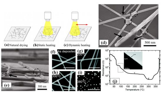
Figure 18.
Schematic diagram of various drying methods. (a) Natural drying. (b) Static heating, (c) Dynamic heating (adapted from [213] with permission from Springer nature 2019). FE-SEM images of AgNW electrodes heated at 200 °C for 20 min having a sheet resistance of 9.5 Ω/sq. (d) Melting and fusion of AgNWs (inside the circles) and the remaining residues (marked by arrows) can be observed in the top view. (e) Tight connections of the AgNWs can be observed in the off-angle cross-sectional view (adapted from [214] with permission from Springer nature 2011). (f–i) Scanning electron microscope (SEM) images of: (f) as-deposited sample and of specimen annealed for 10 min at different temperatures: (g) 200 °C, first occurrence of observable sintering; (h) 300 °C all junctions are sintered; (i) 380 °C complete spheroidization of the network. Image (h) is at a lower magnification than the others to demonstrate that although the nanowires are completely spheroidized the resultant nanoparticles are still aligned at the original position of the wires. The scale bars in images (f,g,i) are 1 μm whereas that of image (h) is 4 μm. (j) Evolution of the electrical resistance of Ag nanowire network during a continuous thermal ramp of 15 °C min−1 from room temperature (associated with deposition solution of 0.75 mg mL−1 and an areal mass density of ≈105 mg m−2). The inset image is a TEM micrograph of a AgNW showing residual PVP from synthesis. (adapted from [215] with permission from Royal Society of Chemistry, 2014).
3.2.3. Mechanical Pressing
Many substrates are susceptible to thermal annealing at high temperatures [212,218,219,220], and mechanical pressing can be used as an alternative when low temperatures are more suitable for TCE fabrication [165,221,222]. Mechanical pressing is a simple technique whereby pressure is applied to enhance the junction conductivity of the AgNW network. Mechanical pressure in the Mega Pascal (MPa) range is commonly used for short time durations. Some researchers also implement hot pressing to control the humidity and temperature [222]. Hot pressing with two rollers at 5 mm/sec was performed three times to enhance the electrical properties of the TCE [223]. Hu and coworkers applied an extremely high mechanical pressure of 81GPa for 50 s to investigate the enhancement in optoelectronic properties. A significant reduction in surface roughness from 110 to 47 nm and Rs by 10 times was observed [182]. Tokuno and coworkers demonstrated that mechanical pressing could enhance optoelectronic properties of heat sensitive materials [214]. They applied 25MPa of mechanical pressure for a time span of 5 s to attain a sheet resistance of 8.6 Ω/sq and 80% transmittance on PET substrates, which cannot be heated at 200 °C. Furthermore, they observed a significant reduction (one-third) in surface roughness as compared to the heat treated electrode. The enhancement in NW-NW junction can be seen from FE-SEM images and the resulting Rs vs. pressure graphs are shown in Figure 19a–c. Du et al. demonstrated that after mechanical pressing Rs can be reduced by one order from 172.89 Ω/sq to 18.6 Ω/sq using a mechanical pressure of 25 MPa [224]. In addition, a sharp contrast in I–V curve characteristics after mechanical pressing was observed as shown in Figure 19d. A further treatment of the AgNW network with UV radiation results in TCE with high FoM (1.35 × 10⁻² Ω−1). Mechanical pressing technique can also be useful in fabricating AgNW based TCFs. He et al. fabricated a PVA-AgNW based TCF using mechanical pressing [156]. The PVA film was first softened by IR radiation followed by inverting the AgNW coated PET onto the PVA film under the application of 30 MPa mechanical pressure for 4 min. A resulting Rs of ~1 Ω/sq at 85% transmittance was reported (Figure 19e,f). A significant increase in the nanowire diameter was observed after mechanically pressing as shown in Figure 19g,h.
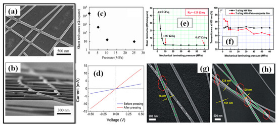
Figure 19.
FE-SEM images of rinsed AgNW electrodes pressed at 25 MPa for 5 s (a) mechanically compressed AgNWs without any residues can be observed in the top view. (b) Tightly connected AgNWs with smooth surfaces can be observed in the off-angle cross-sectional view (c) Sheet resistance of a pressed AgNW electrode after pressing at various applied pressures (d) the I–V characteristics of Ag NWs before and after pressing. (adapted from [214] with permission from Springer nature 2011). (e) Relative plots of the sheet resistance versus the mechanical lamination pressure and (f) Relative plots of the transmittance at 550 nm versus the mechanical lamination pressure. (g) SEM images of the Ag NW film and (h) the Ag NW–PVA composite film on the PET substrate (adapted from [156] with permission from Royal Society of Chemistry, 2014).
3.2.4. Cold Welding
Due to weak metallic bonding, it is quite easy to directly weld metal nanowires by external treatments [225,226]. Although AgNWs have good optoelectronic properties, the presence of an induced nanoscale gap can result in poor NW-NW and NW-substrate contact. Capillarity force can be a good choice while dealing at the nanoscale range [227,228,229]. There have been many publications about using capillarity force as an assembler of nanostructure designs from namomaterials (NPs and NWs) [230,231]. It is worth mentioning that on the nanometer scale, the pulling force of a liquid bridge between two nanowires can reach up to the mega newton range. A simple and quick method of nanowire welding at room temperature has been reported by applying moisture by breathing or water mist [232]. Capillarity force induced by breathing or water mist is an impactful approach for nanowire welding under normal conditions for 30–40 s without annealing as shown in Figure 20h. A negligible variation in transparency with a momentous drop in resistance (from 2.25 × 10⁵ Ω/sq to179 Ω/sq and 6.3 × 10⁴ Ω/sq to 37 Ω/sq) was observed after successive moisture treatments. A schematic for the procedure and observed changes have been shown in Figure 20a–g. Xu et al. synthesized very long nanowires with a maximum length of 200 µm and utilized these nanowires to fabricate a TCE with Rs = 8.6 Ω/sq and T > 91% without any post treatment method. Later they demonstrated a method of AgNW cold welding by dipping the fabricated electrode in CTAB solution for enhancement of transmittance (from 91.3 to 93%) and high FoM [125]. A small decrease in Rs value by scavenging PVP layer was observed by CTAB solution using SERS spectra while the enhanced optoelectronic properties can be seen in Figure 20i. It has also been reported that there is an exceptional wedge-shaped nanoscale gap between the AgNW and substrate, as shown in Figure 20j. This NW-substrate gap plays an important role in the overall Rs. A smart selection of substrate and welding element can improve the results further by improving NW-substrate contact. Zhang et al. used DI water to enhance both NW-NW and NW-substrate contact and demonstrated that a hydrophilic substrate was more efficient as compared to hydrophobic substrate. The capillarity force in case of hydrophilic substrate was more and better NW-substrate contact was obtained, which resulted in a decrease in sheet resistance by 2500 times [233]. A schematic illustration of this mechanism is shown in Figure 20k for better understanding.
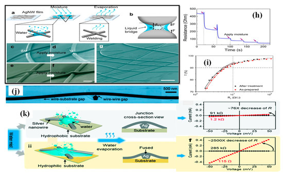
Figure 20.
Capillary-force-induced cold welding of AgNWs. (a) Schematic of moisture treatment for capillary-force-induced cold welding of AgNWs. (b) Schematic of the mechanism of capillary interaction between two particles connected with a liquid bridge. (c–f) Two sets of SEM images of Ag wire-wire junctions before and after moisture treatment. Scale bar: 200 nm. (g) SEM image of a relatively large area of AgNWs showing well welded wire-wire junctions and relatively smooth surface caused by the moisture treatment. Scale bar: 1 μm (h) Resistance of a AgNW film significantly decreases after moisture treatment for a few cycles (adapted from [232] with permission from ACS publications, 2017). (i) A Plot of T versus log Rs for the AgNW-based TEs (adapted from [125] with permission from Elsevier, 2018). (j) SEM image of an AgNW wire–wire junction on a plain substrate. (k)) Illustration of the water-mist treatment process on different substrates for cold-welding) I-V curves of the AgNW junctions before (black dots) and after (red dots) water-mist treatment on hydrophilic glass (bottom) and hydrophobic PET (up) (adapted from [233] with permission from Royal Society of Chemistry, 2018).
3.2.5. Joule Heating and Electro-Deposition Methods
Random arrangement and high surface roughness are the two major drawbacks of nanowire thin films. Recent reports suggested that joule heating by either electric sintering or plasma treatment can enhance the welding of junctions between nanowires [234,235]. Yan and coworkers fabricated a TCE by spray coating AgNWs followed by drop casting GO to enhance the electrical conductivity between nanowires [236]. They performed a post-treatment by using an electrical sintering process which comprised of applying a DC voltage across the TCE to fuse the nanowires at the junction sites which resulted in a decrease in Rs from 1 KΩ/sq to 60 Ω/sq at 86% transmittance. Furthermore, an optimized electric field can also be used to align AgNWs to obtain a TCE with good optoelectronic properties. As a proof of concept, AgNW based TCEs were exposed to different DC voltages to investigate the effect of electric annealing. An abrupt decrease in sheet resistance was observed due to activation of efficient percolating pathways (EPPs). These percolation pathways, as observed under IR surveillance, increased with increasing DC voltage as shown in Figure 21a and resulted in improved contact at the nanowire junction [237].
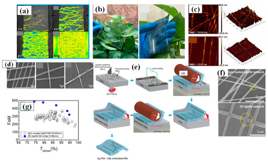
Figure 21.
(a) Image shows the phase signal resulting from all the IR radiations collected during the 5 min cycles at a given voltage (2 V, 4 V, 8 V, 30 V) (adapted from [237] with permission from ACS publications, 2016). (b) Images of two stacked sheets of AgNW flexible electrodes and a sheet of AgNW flexible electrode which is folded through at 180°. (c) AFM images of a pristine AgNW network and regularly arranged AgNW network. The image size is 5 × 5 μm (d) SEM images of without treatment, with plasma treatment of 150 W for 2 min, 200 W for 5 min. (adapted from [238] with permission from Royal Society of Chemistry, 2020). (e) Process of transparent electrode fabrication from Ag NW mixing solution to Ag NW-fully embedded film (adapted from [239] with permission from ACS publications, 2019). (f) SEM images of the AgNW networks before and after electrodeposition. Electrodeposition welds the AgNWs together. (g) FoMs for AgNW networks with initial diameters 80 nm. The FoMs of the ED AgNW networks are superior to those of the as-spin-coated AgNW networks (adapted from [240] with permission from ACS publications, 2020).
Recently, a highly flexible, transparent and conductive electrode with a negligible junction height was fabricated using spray coating under the application of low DC voltage (3.6–6.0 V) as shown in Figure 21b [238]. By utilizing an optimized DC voltage, spray coating time and plasma treatment, they obtained a FoM of 5.52 × 10⁻² Ω−1 with a Rs of 4.64 Ω/sq and 87.3% transmittance. A significant reduction in surface roughness from 16.83 nm to 13 nm was seen after the application of an electric field as shown in Figure 21c–d. Nguyen et al. also used joule heating to reduce the surface roughness of the fabricated TCE to only 1.92 nm and reported a significant decrease of 19% in sheet resistance (9.9 Ω/sq) at 92% transmittance [239]. Later they fabricated an AgNW embedded polyamide composite film by annealing and hot pressing. The ultrasmooth, highly conductive and flexible film peeled from the substrate as illustrated in the schematic in Figure 21e. Another useful post-treatment technique that can be utilized to improve the optoelectronic properties of AgNW based TCE is electrodeposition. In 2019, Lee et.al. used electrodeposition of silver ions on spin coated AgNW TCE and demonstrated that this technique can enhance various optoelectronic properties such as electrical conductivity, optical transmittance, high temperature stability along with low junction height and sheet resistance [240]. Consequently, the obtained a TCE with a transmittance more than 93% and sheet resistance of 14 Ω/sq as shown in Figure 21f,g.
3.2.6. Nanowelding by Chemicals and Polymers
Research studies have also utilized a range of chemicals and polymers to perform nanowelding and enhance the NW-NW junction and NW-substrate contact [23,241,242]. Lu et al. demonstrated alcohol based precursor solution method to create and grow silver “solders” for welding AgNW junctions in order to reduce the junction sheet resistance and enhance stability of the TCE [243]. Briefly, a precursor solution of silver nitrate (AgNO3), nitric acid (HNO3) and ascorbic acid (AA) with a pH of about 3 was prepared in ethanol to use as precursor which completely hinder the reaction between AgNO3 and AA. The fabricated TCE was treated with this precursor solution which induces the capillarity force to enhance the NW-NW junctions as shown in Figure 22a–c. This simple post-treatment method does not require optimization of external parameters such as temperature, humidity, electric current and mechanical pressure and can be performed in normal ambient surrounding. Another effective method of enhancing NW-NW junction is by using hydrogen chloride vapor in the presence of O2 at ambient room temperature [244]. The O2 and HCl vapors act as etching agents and epitaxial recrystallization of Ag atoms occurs at the NW-NW junction under the action of these etching agents. The transition of Ag atoms from one side to other leads a significant decrease in sheet resistance by merging the two nanowires together. The merged planes of the two nanowires can be seen in HRTEM image in Figure 22d–f. Jin and coworkers also demonstrated a method to improve the conductivity of the TCE by using chloride ions, which can efficiently remove the capping agent. They fabricated a composite TCE by coating PET with alginate followed by AgNW solution [209]. This method utilized CaCl2 as an enhancing agent where the Cl− ions removed the PVP coating and decreased the contact resistance between nanowires. Furthermore, Ca2+ being a bivalent cation metal reacted with alginate to enhance the bonding between Alginate and AgNW and form a super hydrophobic gel [245,246]. The treatment reduced the sheet resistance from 300 Ω/sq to 50.3 Ω/sq at a transmittance of 94% and the fabricated composite electrode was highly stable with no observable change in sheet resistance after a tape test. Xiong et al. fabricated an extremely air-stable and conductive FTCE with 8.4 Ω/sq sheet resistance and 86% transmittance on PET by vacuum filtration and transfer method which has been illustrated schematically in Figure 22g [247]. In order to diminish the junction resistance, the AgNW coated PET was primarily cured with electroless welding. The fabricated film was dipped into a solution of glucose and silver–ammonia for an optimized time. A subsequent addition of conductive iongel film obtained by copolymerization of 1-vinyl-3-ethylimidazolium dicynamide and N,N-methylene-bisacrylamide in the presence of ammonium persulfate (APS) was used as a protective layer to enhance the stability of the FTCE in the air without any noticeable increase in sheet resistance as shown in Figure 22h. Recently, Hwang and group fabricated AgNW based TCE with outstanding thermal and ambient stability by encapsulating it with an ultrathin Al2O3 film (around 5.3 nm) via low-temperature (100 °C) atomic layer deposition [248]. The Al2O3-encapsulated TCE were stable even after annealing at 380 °C for 100 min and maintained their electrical and optical properties. The Al2O3 encapsulation layer also effectively blocked the permeation of water molecules, thereby enhancing the ambient stability when exposed to an atmosphere with a relative humidity of 85% at 85 °C for over 1080 h as shown in Figure 22i. The fabricated electrode had 90 ± 3% transmittance and 50 ± 3 Ω/sq sheet resistance with excellent stability against humidity as well as temperature under harsh conditions. The electrode was stable at 400 °C, while the electrode without Al2O3 degraded at 200 °C.
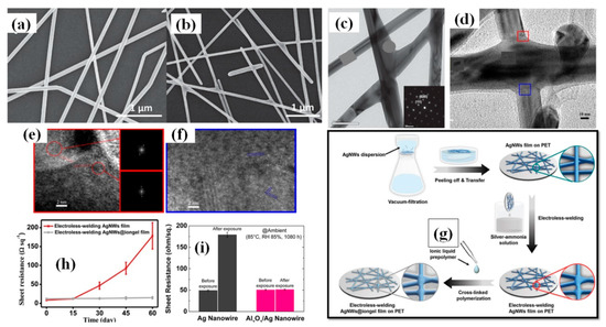
Figure 22.
SEM images of transparent electrodes fabricated from 100 nm AgNWs (a) before and (b) after chemical treatment, (c) TEM image of crossed AgNWsafter chemical treatment better junction can be seen (adapted from [243] with permission from John and Wiley sons 2015). (d) Plane view TEM image of the welded junction between AgNWs. The frames represent the approximate positions of the welded junction for the lattice-resolved TEM in (e,f). Lattice-resolved TEM images of the upper (e) and lower (f) interfaces between the bottom AgNW and the junction, respectively. The upper right and lower right insets in (e) present FFT patterns from the bottom AgNW and the junction, respectively, which are different from each other. Lattice orientation of the junction in (f) mismatches that of the bottom AgNW. (adapted from [244] with permission from ACS publications, 2017). (g). Fabrication of stable AgNWs@iongel composite films for flexible transparent electrodes. (h) The sheet resistance of the electroless-welding AgNWs@iongel film shows tiny change even after exposure in air under ambient conditions for two months, while the sheet resistance of AgNW film without iongel sharply increases after 30 days(adapted from [247] with permission from John and Wiley sons 2016). (i) Sheet resistances of the Ag and Al2O3/Ag nanowire electrodes before and after exposure to ambient conditions with a relative humidity of 85% at 85 °C for 1080 h (adapted from [248] with permission from Springer, 2017).
3.2.7. Light Induced Welding
Light induced welding has been utilized as a simple and time efficient post-treatment method to improve AgNW based TCE performance. The intensity of the light and treatment time are two important parameters while using light induced welding methods. Some researchers have studied the effect of sunlight to enhance the properties of the TCE [249]. The light intensity was controlled by a solar simulator, and could be further enhanced by using light converging lenses. They exposed the fabricated electrode to sunlight for 4 h to enhance the NW-NW junction contact and the results were satisfactory (T ~87% and Rs < 20 Ω/sq). However these results were superior to the results of thermal annealing at 200 °C as presented in Figure 23a. Silver nanostructures are susceptible to light; various morphological changes have been observed when they are exposed to various light sources [250]. Lee et al. demonstrated that a selective laser nano-welding was much more efficient in terms of processing speed as well as thermal controllability, as compared to broadband lamp welding. Since lasers are monochromatic sources of light whereby photon energy can be controlled, the treatment temperature can be accurately controlled depending on the substrate used. The occurrence of surface Plasmon resonance of nanowires and enhancement in electrical properties at the NW-NW junction can be seen in the FE-SEM images in Figure 23b. It is worth mentioning that the results obtained from the laser nanowelding technique were far better than those resulting from annealing at 250 °C, as shown in Figure 23c. High intensity pulsed light sintering technique can also be used in order to attain good electrical conductivity in a short time period. Jiu et al. fabricated an AgNW based TCE on PET using Mayer rod coating followed by HIPL treatment to enhance the properties of the TCE by varying the light energy from 0.21–2.33 J/cm2 [248]. Improved contact at the NW-NW and NW-substrate junction was observed at 1.14 J/cm2, while the nanowire morphology was critically damaged at 2.33 J/cm2, as shown in Figure 23d. Light induced nanowelding is an effective treatment method for Ag nanowires to interconnect at the junctions. The light induced heat energy efficiently enhances the junction geometry in such a way that the planes of nanowires completely merge with each other due to the heat generation in highly compact AgNW network. A complete epitaxial recrystallization of Ag atoms to make twinned planes by merging two planes under plasmonic nanowelding at the NW-NW junction can be seen in the TEM and SAED patterns in Figure 23e–h [251]. The light exposure time span is a critical parameter when dealing with high energy irradiation. In order to minimize the thermal damage, an ultrafast femtosecond laser nanowelding of AgNWs was demonstrated [252]. Limited thermal diffusion and localized field enhancement combined with femtosecond lasers enables the maintenance of the original crystal structure while enhancing junction electrical properties. The fabricated electrode after enhancement results in 94% transmittance and 25 Ω/sq sheet resistance. A comparative study with other heating methods is shown in Figure 23j. Recently, research efforts have also been made to accomplish fast AgNW sintering at low cost using a xenon flash lamp [158]. Improved optoelectronic properties on a stretchable PDMS electrode were achieved after xenon flash lamp treatment as shown below in Figure 23i.
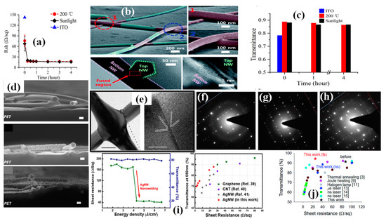
Figure 23.
(a) Sheet resistance (Rsh) as a function of treatment time for samples treated with Sun sunlight illumination (black diamonds) and thermal annealing at 200 °C (red circles), respectively. (adapted from [249] with permission from Springer nature, 2017). (b) Magnified SEM (pseudo-colored) and HRTEM images Laser nano-welding of very long Ag NW network electrodes for highly transparent and flexible electrodes. (adapted from [164] with permission from Royal society of chemistry 2012). (c) Histogram of the light transmittance at 550 nm before and after different periods of time for both treatment methods (ref. [250])Cross-sectional SEM images of AgNW films on PET substrates (d) before and after HIPL sintering with light intensities of 1.14 and 2.33 Jcm−2, respectively. (adapted from [248] with permission from Springer nature, 2017). (e)TEM images of AgNW junctions after optical welding, merged planes can be seen in HRTEM image (f) SAED pattern of the top nanowire away from the junction. The large number of double diffractions caused by the pentagonally twinned cross-section lead to prominent lines of spots in only one direction, parallel to the blue line (g) SAED pattern of the bottom nanowire away from the junction. The double diffraction spots occur in a direction roughly perpendicular to that in b and parallel to the red line. (h) SAED pattern of the junction. Both sets of spots from b and c are visible. The double diffraction spots create a grid instead of an array of parallel lines as in g and h. (adapted from [251] with permission from Springer nature, 2012). (i) Sheet resistance and transmittance response to the flash light method induced nanowelding and Resulting sheet resistance and transmittance values compared to reference values from literature Improved optoelectronic properties on a stretchable PDMS electrode were achieved after xenon flash lamp treatment as shown in Figure 23i. (adapted from [253] with permission from Royal society of chemistry, 2016). (j) Comparison of the transmittance and sheet resistance with the previously reported results (adapted from [158] with permission from Springer nature 2018).
4. Conclusions and Future Outlooks
Herein, we discussed the various AgNW synthesis protocols and strategies used for fabricating TCE with improved optoelectronic properties. In recent years, the polyol method has been widely used for AgNW synthesis with good control over nanowire morphology. While this method possesses various advantages like simplicity and scalability, the use of organic surfactants like PVP can degrade the optoelectronic performance of the fabricated TCE, resulting in a hydrophilic surface. Furthermore, optimization of the polyol process is critical to ensure that all Ag seeds are transformed into nanowires, as these seeds can agglomerate together with the nanowires after centrifugation. Besides centrifugation, researchers have also used cross flow purification and decantation to remove organic and inorganic contaminants [255,256]. Some researchers have utilized millifluidic reactor systems for AgNW synthesis in order to better control the chemical potential, supersaturation state and nanowire aspect ratio [127,257]. Characterization techniques like X-ray adsorption spectroscopy (XAS) have also been utilized to investigate the growth mechanism and reaction dynamics during AgNW synthesis, thus enabling improved control over the final nanowire morphology [258]. Furthermore, efforts have been made to enable green AgNW synthesis where the chemical reagents are biocompatible and can be easily disposed of [259]. Since AgNWs are prone to oxidation in air, researchers have also tried coating them with polymers and anti-oxidative metals like gold by making core shell structures [260,261,262,263,264,265]. While AgNW based TCE have several advantages including scalable solution based processing capability, low sheet resistance, high conductivity, low surface roughness and mechanical flexibility and stretchability, there are still some issues that need to be resolved; for example, the non-uniform distribution of the AgNW network obtained during solution based deposition can lead to localized joule heating, which can degrade optoelectronic performance [266]. Optimization of deposition parameters is key to ensure uniform AgNW distribution on the substrate surface. Finally, progress and optoelectronic enhancement of AgNW based TCE will enable a range of applications, from flexible optoelectronics to wearable devices [267,268]. While this review is primarily focused on synthesis of AgNW and techniques to fabricate AgNW based TCE, there has also been widespread research interest in utilizing these TCE for optoelectronic applications, including electronic skins [19,118], smart clothes [20], organic field effect transistors [269,270], wearable heaters [21,22], organic memory devices [271,272], flexible display panels [28], foldable displays [23,24,25,26], organic solar cells [219,273], smart windows [17,18], organics light emitting diodes [274,275], light emitting electro chemical cells [26,276] and compliant solar cells [27], among others. In summary, owing to their superior thermal and electrical conductivity, AgNW based TCEs are expected to play a key role in the future in a range of novel nano-optoelectronic applications.
Author Contributions
All the authors with relation to this paper have made substantial contributions to publish this works. A.K. has worked on resources and data collection for review and prepared the draft of the manuscript under the guidance of C.-H.C. and M.O.S. C.-H.C. and A.K. have worked on defining the methodology for review writing. M.O.S. has worked on writing the conclusion and future work along with refining, reviewing and editing the manuscript with formal analysis. All authors have read and agreed to the published version of the manuscript.
Funding
This research received no external funding.
Data Availability Statement
Data sharing not applicable.
Conflicts of Interest
The authors declare no conflict of interest.
References
- Zhao, J.; Buia, C.; Han, J.; Lu, J.P. Quantum transport properties of ultrathin silver nanowires. Nanotechnology 2003, 14, 501. [Google Scholar] [CrossRef]
- Dresselhaus, M.S.; Lin, Y.-M.; Rabin, O.; Black, M.R.; Kong, J.; Dresselhaus, G. Nanowires. In Springer Handbook of Nanotechnology; Springer: Berlin/Heidelberg, Germany, 2010; pp. 119–167. [Google Scholar]
- Rodrigues, V.; Bettini, J.; Rocha, A.R.; Rego, L.G.C.; Ugarte, D. Quantum conductance in silver nanowires: Correlation between atomic structure and transport properties. Phys. Rev. B 2002, 65, 153402. [Google Scholar] [CrossRef]
- Zhang, R.; Engholm, M. Recent progress on the fabrication and properties of silver nanowire-based transparent electrodes. Nanomaterials 2018, 8, 628. [Google Scholar] [CrossRef]
- Yin, X.; Kumar, S. Flow visualization of the liquid emptying process in scaled-up gravure grooves and cells. Chem. Eng. Sci. 2006, 61, 1146–1156. [Google Scholar] [CrossRef]
- Wang, L.; Gao, X.; Jin, L.; Wu, Q.; Chen, Z.; Lin, X. Amperometric glucose biosensor based on silver nanowires and glucose oxidase. Sens. Actuators B Chem. 2013, 176, 9–14. [Google Scholar] [CrossRef]
- Jones, R.S.; Draheim, R.R.; Roldo, M. Silver nanowires: Synthesis, antibacterial activity and biomedical applications. Appl. Sci. 2018, 8, 673. [Google Scholar] [CrossRef]
- Lee, H.; Kim, M.; Kim, I.; Lee, H. Flexible and stretchable optoelectronic devices using silver nanowires and graphene. Adv. Mater. 2016, 28, 4541–4548. [Google Scholar] [CrossRef] [PubMed]
- Karthik, P.S.; Singh, S.P. Conductive silver inks and their applications in printed and flexible electronics. RSC Adv. 2015, 5, 77760–77790. [Google Scholar]
- Dahiya, R.; Yogeswaran, N.; Liu, F.; Manjakkal, L.; Burdet, E.; Hayward, V.; Jörntell, H. Large-area soft e-skin: The challenges beyond sensor designs. Proc. IEEE 2019, 107, 2016–2033. [Google Scholar] [CrossRef]
- Kostowskyj, M.A.; Gilliam, R.J.; Kirk, D.W.; Thorpe, S.J. Silver nanowire catalysts for alkaline fuel cells. Int. J. Hydrog. Energy 2008, 33, 5773–5778. [Google Scholar] [CrossRef]
- Liang, X.; Zhao, T.; Jiang, W.; Yu, X.; Hu, Y.; Zhu, P.; Zheng, H.; Sun, R.; Wong, C.-P. Highly transparent triboelectric nanogenerator utilizing in-situ chemically welded silver nanowire network as electrode for mechanical energy harvesting and body motion monitoring. Nano Energy 2019, 59, 508–516. [Google Scholar] [CrossRef]
- Li, W.; Zhang, H.; Shi, S.; Xu, J.; Qin, X.; He, Q.; Yang, K.; Dai, W.; Liu, G.; Zhou, Q. Recent progress in silver nanowire networks for flexible organic electronics. J. Mater. Chem. C 2020, 8, 4636–4674. [Google Scholar] [CrossRef]
- Huo, D.; Kim, M.J.; Lyu, Z.; Shi, Y.; Wiley, B.J.; Xia, Y. One-dimensional metal nanostructures: From colloidal syntheses to applications. Chem. Rev. 2019, 119, 8972–9073. [Google Scholar] [CrossRef]
- Huang, Q.; Zhu, Y. Printing conductive nanomaterials for flexible and stretchable electronics: A review of materials, processes, and applications. Adv. Mater. Technol. 2019, 4, 1800546. [Google Scholar] [CrossRef]
- Kwon, J.; Suh, Y.D.; Lee, J.; Lee, P.; Han, S.; Hong, S.; Yeo, J.; Lee, H.; Ko, S.H. Recent progress in silver nanowire based flexible/wearable optoelectronics. J. Mater. Chem. C 2018, 6, 7445–7461. [Google Scholar] [CrossRef]
- Park, J.-Y.; Kim, H.-K. Highly stretchable polymer-dispersed liquid crystal-based smart windows with transparent and stretchable hybrid electrodes. RSC Adv. 2018, 8, 36549–36557. [Google Scholar] [CrossRef]
- Mallikarjuna, K.; Kim, H. Highly transparent conductive reduced graphene oxide/silver nanowires/silver grid electrodes for low-voltage electrochromic smart windows. ACS Appl. Mater. Interfaces 2018, 11, 1969–1978. [Google Scholar] [CrossRef]
- Lipomi, D.J.; Vosgueritchian, M.; Tee, B.C.; Hellstrom, S.L.; Lee, J.A.; Fox, C.H.; Bao, Z. Skin-like pressure and strain sensors based on transparent elastic films of carbon nanotubes. Nat. Nanotechnol. 2011, 6, 788–792. [Google Scholar] [CrossRef]
- Hu, B.; Li, D.; Ala, O.; Manandhar, P.; Fan, Q.; Kasilingam, D.; Calvert, P.D. Textile-Based Flexible Electroluminescent Devices. Adv. Funct. Mater. 2011, 21, 305–311. [Google Scholar] [CrossRef]
- Choi, S.; Park, J.; Hyun, W.; Kim, J.; Kim, J.; Lee, Y.B.; Song, C.; Hwang, H.J.; Kim, J.H.; Hyeon, T. Stretchable heater using ligand-exchanged silver nanowire nanocomposite for wearable articular thermotherapy. ACS Nano 2015, 9, 6626–6633. [Google Scholar] [CrossRef] [PubMed]
- Hong, S.; Lee, H.; Lee, J.; Kwon, J.; Han, S.; Suh, Y.D.; Cho, H.; Shin, J.; Yeo, J.; Ko, S.H. Highly stretchable and transparent metal nanowire heater for wearable electronics applications. Adv. Mater. 2015, 27, 4744–4751. [Google Scholar] [CrossRef] [PubMed]
- Liang, J.; Li, L.; Tong, K.; Ren, Z.; Hu, W.; Niu, X.; Chen, Y.; Pei, Q. Silver nanowire percolation network soldered with graphene oxide at room temperature and its application for fully stretchable polymer light-emitting diodes. ACS Nano 2014, 8, 1590–1600. [Google Scholar] [CrossRef]
- Miller, M.S.; O’Kane, J.C.; Niec, A.; Carmichael, R.S.; Carmichael, T.B. Silver nanowire/optical adhesive coatings as transparent electrodes for flexible electronics. ACS Appl. Mater. Interfaces 2013, 5, 10165–10172. [Google Scholar] [CrossRef]
- Wang, J.; Yan, C.; Cai, G.; Cui, M.; Lee-Sie Eh, A.; See Lee, P. Extremely stretchable electroluminescent devices with ionic conductors. Adv. Mater. 2016, 28, 4490–4496. [Google Scholar] [CrossRef] [PubMed]
- Liang, J.; Li, L.; Niu, X.; Yu, Z.; Pei, Q. Elastomeric polymer light-emitting devices and displays. Nat. Photonics 2013, 7, 817–824. [Google Scholar] [CrossRef]
- Lipomi, D.J.; Tee, B.C.K.; Vosgueritchian, M.; Bao, Z. Stretchable organic solar cells. Adv. Mater. 2011, 23, 1771–1775. [Google Scholar] [CrossRef]
- Wang, J.; Liang, M.; Fang, Y.; Qiu, T.; Zhang, J.; Zhi, L. Rod-coating: Towards large-area fabrication of uniform reduced graphene oxide films for flexible touch screens. Adv. Mater. 2012, 24, 2874–2878. [Google Scholar] [CrossRef]
- Langley, D.; Giusti, G.; Mayousse, C.; Celle, C.; Bellet, D.; Simonato, J.-P. Flexible transparent conductive materials based on silver nanowire networks: A review. Nanotechnology 2013, 24, 452001. [Google Scholar] [CrossRef]
- Basarir, F.; Irani, F.S.; Kosemen, A.; Camic, B.T.; Oytun, F.; Tunaboylu, B.; Shin, H.J.; Nam, K.Y.; Choi, H. Recent progresses on solution-processed silver nanowire based transparent conducting electrodes for organic solar cells. Mater. Today Chem. 2017, 3, 60–72. [Google Scholar] [CrossRef]
- Kumar, A.; Zhou, C. The race to replace tin-doped indium oxide: Which material will win? ACS Nano 2010, 4, 11–14. [Google Scholar] [CrossRef]
- Zhang, P.; Wyman, I.; Hu, J.; Lin, S.; Zhong, Z.; Tu, Y.; Huang, Z.; Wei, Y. Silver nanowires: Synthesis technologies, growth mechanism and multifunctional applications. Mater. Sci. Eng. B 2017, 223, 1–23. [Google Scholar] [CrossRef]
- Hecht, D.S.; Hu, L.; Irvin, G. Emerging transparent electrodes based on thin films of carbon nanotubes, graphene, and metallic nanostructures. Adv. Mater. 2011, 23, 1482–1513. [Google Scholar] [CrossRef] [PubMed]
- Xiang, X.-Z.; Gong, W.-Y.; Kuang, M.-S.; Wang, L. Progress in application and preparation of silver nanowires. Rare Met. 2016, 35, 289–298. [Google Scholar] [CrossRef]
- Abbasi, N.M.; Yu, H.; Wang, L.; Amer, W.A.; Akram, M.; Khalid, H.; Chen, Y.; Saleem, M.; Sun, R.; Shan, J. Preparation of silver nanowires and their application in conducting polymer nanocomposites. Mater. Chem. Phys. 2015, 166, 1–15. [Google Scholar] [CrossRef]
- Sun, Y. Silver nanowires–unique templates for functional nanostructures. Nanoscale 2010, 2, 1626–1642. [Google Scholar] [CrossRef] [PubMed]
- He, W.; Ye, C. Flexible transparent conductive films on the basis of Ag nanowires: Design and applications: A review. J. Mater. Sci. Technol. 2015, 31, 581–588. [Google Scholar] [CrossRef]
- Huczko, A. Template-based synthesis of nanomaterials. Appl. Phys. A 2000, 70, 365–376. [Google Scholar] [CrossRef]
- Pourahmad, A.; Sohrabnezhad, S. Preparation and characterization of Ag nanowires in mesoporous MCM-41 nanoparticles template by chemical reduction method. J. Alloys Compd. 2009, 484, 314–316. [Google Scholar] [CrossRef]
- Ajayan, P.M. Capillarity-induced filling of carbon nanotubes. Nature 1993, 361, 333–334. [Google Scholar] [CrossRef]
- Ugarte, D.; Chatelain, A.; De Heer, W.A. Nanocapillarity and chemistry in carbon nanotubes. Science 1996, 274, 1897–1899. [Google Scholar] [CrossRef]
- Han, Y.-J.; Kim, J.M.; Stucky, G.D. Preparation of noble metal nanowires using hexagonal mesoporous silica SBA-15. Chem. Mater. 2000, 12, 2068–2069. [Google Scholar] [CrossRef]
- Takai, A.; Doi, Y.; Yamauchi, Y.; Kuroda, K. Soft-chemical approach of noble metal nanowires templated from mesoporous silica (SBA-15) through vapor infiltration of a reducing agent. J. Phys. Chem. C 2010, 114, 7586–7593. [Google Scholar] [CrossRef]
- Kim, K.-J.; Lee, E.-S.; Kwon, Y.-U. Syntheses of micrometer-long Pt and Ag nanowires through SBA-15 templating. J. Nanoparticle Res. 2012, 14, 1270. [Google Scholar] [CrossRef]
- Zimmermann, R.M.; Cox, E.C. DNA stretching on functionalized gold surfaces. Nucleic Acids Res. 1994, 22, 492–497. [Google Scholar] [CrossRef] [PubMed]
- Bensimon, A.; Simon, A.; Chiffaudel, A.; Croquette, V.; Heslot, F.; Bensimon, D. Alignment and sensitive detection of DNA by a moving interface. Science 1994, 265, 2096–2098. [Google Scholar] [CrossRef] [PubMed]
- Watson, J.D.; Hopkins, N.H.; Roberts, J.W.; Steitz, J.A.; Weiner, A.M. Molecular Biology of the Gene, 4th ed.; lknjamin/Cumminp Pub. Co.: Menlo Park, CA, USA, 1987. [Google Scholar]
- Lehn, J.M. Supramolecular Chemistry: Concepts and Perspectives; VCH Veragsgesellschaft: Weinheim, Germany, 1995. [Google Scholar]
- Braun, E.; Eichen, Y.; Sivan, U.; Ben-Yoseph, G. DNA-templated assembly and electrode attachment of a conducting silver wire. Nature 1998, 391, 775–778. [Google Scholar] [CrossRef] [PubMed]
- Berti, L.; Alessandrini, A.; Facci, P. DNA-templated photoinduced silver deposition. J. Am. Chem. Soc. 2005, 127, 11216–11217. [Google Scholar] [CrossRef]
- Lu, J.; Yang, L.; Xie, A.; Shen, Y. DNA-templated photo-induced silver nanowires: Fabrication and use in detection of relative humidity. Biophys. Chem. 2009, 145, 91–97. [Google Scholar] [CrossRef] [PubMed]
- Vilayurganapathy, S.; Nandasiri, M.I.; Joly, A.G.; El-Khoury, P.Z.; Varga, T.; Coffey, G.; Schwenzer, B.; Pandey, A.; Kayani, A.; Hess, W.P. Silver nanorod arrays for photocathode applications. Appl. Phys. Lett. 2013, 103, 161112. [Google Scholar] [CrossRef]
- Sauer, G.; Brehm, G.; Schneider, S.; Nielsch, K.; Wehrspohn, R.B.; Choi, J.; Hofmeister, H.; Gösele, U. Highly ordered monocrystalline silver nanowire arrays. J. Appl. Phys. 2002, 91, 3243–3247. [Google Scholar] [CrossRef]
- Zhang, C.; Li, C.; Si, X.; He, Z.; Qi, J.; Feng, J.; Cao, J. Single-crystalline silver nanowire arrays directly synthesized onto substrates by template-assisted chemical wetting. Materialia 2020, 9, 100529. [Google Scholar] [CrossRef]
- Hong, B.H.; Bae, S.C.; Lee, C.-W.; Jeong, S.; Kim, K.S. Ultrathin single-crystalline silver nanowire arrays formed in an ambient solution phase. Science 2001, 294, 348–351. [Google Scholar] [CrossRef]
- Bhattacharrya, S.; Saha, S.K.; Chakravorty, D. Nanowire formation in a polymeric film. Appl. Phys. Lett. 2000, 76, 3896–3898. [Google Scholar] [CrossRef]
- Tao, L.; Huo, Z.; Dai, S.; Ding, Y.; Zhu, J.; Zhang, C.; Zhang, B.; Yao, J.; Nazeeruddin, M.K.; Grätzel, M. Stable quasi-solid-state dye-sensitized solar cells using novel low molecular mass organogelators and room-temperature molten salts. J. Phys. Chem. C 2014, 118, 16718–16726. [Google Scholar] [CrossRef]
- Jin, Q.; Zhang, L.; Cao, H.; Wang, T.; Zhu, X.; Jiang, J.; Liu, M. Self-assembly of copper (II) ion-mediated nanotube and its supramolecular chiral catalytic behavior. Langmuir 2011, 27, 13847–13853. [Google Scholar] [CrossRef] [PubMed]
- Nguyen, N.-T.; Liu, J.-H. Wet chemical synthesis of silver nanowires based on a soft template of cholesteryl pyridine carbamate organogel. Sci. Adv. Mater. 2015, 7, 1282–1290. [Google Scholar] [CrossRef]
- Liu, C.Y.; Zhang, Y.S.; Kao, C.K.; Liu, J.-H. Fabrication of silver nanowires via a β-cyclodextrin-derived soft template. Express Polym. Lett. 2018, 12, 591–599. [Google Scholar] [CrossRef]
- Majumder, J.; Deb, J.; Das, M.R.; Jana, S.S.; Dastidar, P. Designing a simple organic salt-based supramolecular topical gel capable of displaying in vivo self-delivery application. Chem. Commun. 2014, 50, 1671–1674. [Google Scholar] [CrossRef]
- Eisele, D.M.; Berlepsch, H.V.; Bottcher, C.; Stevenson, K.J.; Vanden Bout, D.A.; Kirstein, S.; Rabe, J.R.P. Photoinitiated growth of sub-7 nm silver nanowires within a chemically active organic nanotubular template. J. Am. Chem. Soc. 2010, 132, 2104–2105. [Google Scholar] [CrossRef] [PubMed]
- Cölfen, H. Double-hydrophilic block copolymers: Synthesis and application as novel surfactants and crystal growth modifiers. Macromol. Rapid Commun. 2001, 22, 219–252. [Google Scholar] [CrossRef]
- Zhang, D.; Qi, L.; Ma, J.; Cheng, H. Formation of silver nanowires in aqueous solutions of a double-hydrophilic block copolymer. Chem. Mater. 2001, 13, 2753–2755. [Google Scholar] [CrossRef]
- Jana, N.R.; Gearheart, L.; Murphy, C.J. Wet chemical synthesis of silver nanorods and nanowires of controllable aspect ratioElectronic supplementary information (ESI) available: UV–VIS spectra of silver nanorods. Chem. Commun. 2001, 7, 617–618. Available online: http://www.rsc.org/suppdata/cc/b1/b100521i (accessed on 9 March 2021). [CrossRef]
- Mastai, Y.; Polsky, R.; Koltypin, Y.; Gedanken, A.; Hodes, G. Pulsed sonoelectrochemical synthesis of cadmium selenide nanoparticles. J. Am. Chem. Soc. 1999, 121, 10047–10052. [Google Scholar] [CrossRef]
- Mastai, Y.; Homyonfer, M.; Gedanken, A.; Hodes, G. Room Temperature Sonoelectrochemical Synthesis of Molybdenum Sulfide Fullerene-Like Nanoparticles. Adv. Mater. 1999, 11, 1010–1013. [Google Scholar] [CrossRef]
- Zhu, J.-J.; Qiu, Q.-F.; Wang, H.; Zhang, J.-R.; Zhu, J.-M.; Chen, Z.-Q. Synthesis of silver nanowires by a sonoelectrochemical method. Inorg. Chem. Commun. 2002, 5, 242–244. [Google Scholar] [CrossRef]
- Zhang, D.; Qi, L.; Yang, J.; Ma, J.; Cheng, H.; Huang, L. Wet chemical synthesis of silver nanowire thin films at ambient temperature. Chem. Mater. 2004, 16, 872–876. [Google Scholar] [CrossRef]
- Liu, S.; Yue, J.; Gedanken, A. Synthesis of long silver nanowires from AgBr nanocrystals. Adv. Mater. 2001, 13, 656–658. [Google Scholar] [CrossRef]
- Caswell, K.K.; Bender, C.M.; Murphy, C.J. Seedless, Surfactantless Wet Chemical Synthesis of Silver Nanowires. Nano Lett. 2003, 3, 667–669. [Google Scholar] [CrossRef]
- Wang, Z.; Liu, J.; Chen, X.; Wan, J.; Qian, Y. A Simple Hydrothermal Route to Large-Scale Synthesis of Uniform Silver Nanowires. Chem. Eur. J. 2005, 11, 160–163. [Google Scholar] [CrossRef]
- Xu, J.; Hu, J.; Peng, C.; Liu, H.; Hu, Y. A simple approach to the synthesis of silver nanowires by hydrothermal process in the presence of gemini surfactant. J. Colloid Interface Sci. 2006, 298, 689–693. [Google Scholar] [CrossRef]
- Bari, B.; Lee, J.; Jang, T.; Won, P.; Ko, S.H.; Alamgir, K.; Arshad, M.; Guo, L.J. Simple hydrothermal synthesis of very-long and thin silver nanowires and their application in high quality transparent electrodes. J. Mater. Chem. A 2016, 4, 11365–11371. [Google Scholar] [CrossRef]
- Fiévet, F.; Ammar-Merah, S.; Brayner, R.; Chau, F.; Giraud, M.; Mammeri, F.; Peron, J.; Piquemal, J.Y.; Sicard, L.; Viau, G. The polyol process: A unique method for easy access to metal nanoparticles with tailored sizes, shapes and compositions. Chem. Soc. Rev. 2018, 47, 5187–5233. [Google Scholar] [CrossRef] [PubMed]
- Shen, Q.; Min, Q.; Shi, J.; Jiang, L.; Zhang, J.-R.; Hou, W.; Zhu, J.-J. Morphology-controlled synthesis of palladium nanostructures by sonoelectrochemical method and their application in direct alcohol oxidation. J. Phys. Chem. C 2009, 113, 1267–1273. [Google Scholar] [CrossRef]
- Chandran, S.P.; Chaudhary, M.; Pasricha, R.; Ahmad, A.; Sastry, M. Synthesis of gold nanotriangles and silver nanoparticles using Aloevera plant extract. Biotechnol. Prog. 2006, 22, 577–583. [Google Scholar] [CrossRef]
- Wiley, B.; Sun, Y.; Mayers, B.; Xia, Y. Shape-controlled synthesis of metal nanostructures: The case of silver. Chem. Eur. J. 2005, 11, 454–463. [Google Scholar] [CrossRef]
- Xia, Y.; Xia, X.; Peng, H.-C. Shape-controlled synthesis of colloidal metal nanocrystals: Thermodynamic versus kinetic products. J. Am. Chem. Soc. 2015, 137, 7947–7966. [Google Scholar] [CrossRef] [PubMed]
- Campbell, C.T. Ultrathin metal films and particles on oxide surfaces: Structural, electronic and chemisorptive properties. Surf. Sci. Rep. 1997, 27, 1–111. [Google Scholar] [CrossRef]
- Sexton, B.A.; Madix, R.J. Vibrational spectra of molecular and atomic oxygen on Ag (11O). Chem. Phys. Lett. 1980, 76, 294–297. [Google Scholar] [CrossRef]
- Sun, Y.; Gates, B.; Mayers, B.; Xia, Y. Crystalline silver nanowires by soft solution processing. Nano Lett. 2002, 2, 165–168. [Google Scholar] [CrossRef]
- Sun, Y.; Yin, Y.; Mayers, B.T.; Herricks, T.; Xia, Y. Uniform silver nanowires synthesis by reducing AgNO3 with ethylene glycol in the presence of seeds and poly (vinyl pyrrolidone). Chem. Mater. 2002, 14, 4736–4745. [Google Scholar] [CrossRef]
- Sun, Y.; Xia, Y. Large-scale synthesis of uniform silver nanowires through a soft, self-seeding, polyol process. Adv. Mater. 2002, 14, 833–837. [Google Scholar] [CrossRef]
- Wiley, B.J.; Chen, Y.; McLellan, J.M.; Xiong, Y.; Li, Z.-Y.; Ginger, D.; Xia, Y. Synthesis and optical properties of silver nanobars and nanorice. Nano Lett. 2007, 7, 1032–1036. [Google Scholar] [CrossRef]
- Khatoon, U.T.; Rao, G.V.S.N.; Mantravadi, K.M.; Oztekin, Y. Strategies to synthesize various nanostructures of silver and their applications—A review. RSC Adv. 2018, 8, 19739–19753. [Google Scholar] [CrossRef]
- Chen, J.; Herricks, T.; Geissler, M.; Xia, Y. Single-crystal nanowires of platinum can be synthesized by controlling the reaction rate of a polyol process. J. Am. Chem. Soc. 2004, 126, 10854–10855. [Google Scholar] [CrossRef]
- Korte, K.E.; Skrabalak, S.E.; Xia, Y. Rapid synthesis of silver nanowires through a CuCl-or CuCl 2-mediated polyol process. J. Mater. Chem. 2008, 18, 437–441. [Google Scholar] [CrossRef]
- Wiley, B.; Sun, Y.; Xia, Y. Polyol synthesis of silver nanostructures: Control of product morphology with Fe (II) or Fe (III) species. Langmuir 2005, 21, 8077–8080. [Google Scholar] [CrossRef]
- Wiley, B.; Sun, Y.; Xia, Y. Synthesis of silver nanostructures with controlled shapes and properties. Acc. Chem. Res. 2007, 40, 1067–1076. [Google Scholar] [CrossRef]
- Iijima, S.; Ichihashi, T. Structural instability of ultrafine particles of metals. Phys. Rev. Lett. 1986, 56, 616. [Google Scholar] [CrossRef]
- Smith, D.J.; Petford-Long, A.K.; Wallenberg, L.R.; Bovin, J.O. Dynamic atomic-level rearrangements in small gold particles. Science 1986, 233, 872–875. [Google Scholar] [CrossRef] [PubMed]
- Ajayan, P.M.; Marks, L.D. Quasimelting and phases of small particles. Phys. Rev. Lett. 1988, 60, 585. [Google Scholar] [CrossRef] [PubMed]
- Cleveland, C.L.; Landman, U. The energetics and structure of nickel clusters: Size dependence. J. Chem. Phys. 1991, 94, 7376–7396. [Google Scholar] [CrossRef]
- Johnson, C.J.; Dujardin, E.; Davis, S.A.; Murphy, C.J.; Mann, S. Growth and form of gold nanorods prepared by seed-mediated, surfactant-directed synthesis. J. Mater. Chem. 2002, 12, 1765–1770. [Google Scholar] [CrossRef]
- Sun, Y.; Mayers, B.; Herricks, T.; Xia, Y. Polyol synthesis of uniform silver nanowires: A plausible growth mechanism and the supporting evidence. Nano Lett. 2003, 3, 955–960. [Google Scholar] [CrossRef]
- Chen, H.; Gao, Y.; Zhang, H.; Liu, L.; Yu, H.; Tian, H.; Xie, S.; Li, J. Transmission-electron-microscopy study on fivefold twinned silver nanorods. J. Phys. Chem. B 2004, 108, 12038–12043. [Google Scholar] [CrossRef]
- Wiley, B.; Herricks, T.; Sun, Y.; Xia, Y. Polyol synthesis of silver nanoparticles: Use of chloride and oxygen to promote the formation of single-crystal, truncated cubes and tetrahedrons. Nano Lett. 2004, 4, 1733–1739. [Google Scholar] [CrossRef]
- Im, S.H.; Lee, Y.T.; Wiley, B.; Xia, Y. Large-scale synthesis of silver nanocubes: The role of hcl in promoting cube perfection and monodispersity. Angew. Chem. Int. Ed. 2005, 44, 2154–2157. [Google Scholar] [CrossRef]
- Schuette, W.M.; Buhro, W.E. Polyol synthesis of silver nanowires by heterogeneous nucleation; mechanistic aspects influencing nanowire diameter and length. Chem. Mater. 2014, 26, 6410–6417. [Google Scholar] [CrossRef]
- Coskun, S.; Aksoy, B.; Unalan, H.E. Polyol synthesis of silver nanowires: An extensive parametric study. Cryst. Growth Des. 2011, 11, 4963–4969. [Google Scholar] [CrossRef]
- Lee, J.H.; Lee, P.; Lee, D.; Lee, S.S.; Ko, S.H. Large-scale synthesis and characterization of very long silver nanowires via successive multistep growth. Cryst. Growth Des. 2012, 12, 5598–5605. [Google Scholar] [CrossRef]
- Lin, J.-Y.; Hsueh, Y.-L.; Huang, J.-J.; Wu, J.-R. Effect of silver nitrate concentration of silver nanowires synthesized using a polyol method and their application as transparent conductive films. Thin Solid Film. 2015, 584, 243–247. [Google Scholar] [CrossRef]
- Ma, J.; Zhan, M. Rapid production of silver nanowires based on high concentration of AgNO3 precursor and use of FeCl3 as reaction promoter. RSC Adv. 2014, 4, 21060–21071. [Google Scholar] [CrossRef]
- Ran, Y.; He, W.; Wang, K.; Ji, S.; Ye, C. A one-step route to Ag nanowires with a diameter below 40 nm and an aspect ratio above 1000. Chem. Commun. 2014, 50, 14877–14880. [Google Scholar] [CrossRef]
- Mullin, J.W. Crystallization; Elsevier: Amsterdam, The Netherlands, 2001. [Google Scholar]
- Yang, L.; Zhang, T.; Zhou, H.; Price, S.C.; Wiley, B.J.; You, W. Solution-processed flexible polymer solar cells with silver nanowire electrodes. ACS Appl. Mater. Interfaces 2011, 3, 4075–4084. [Google Scholar] [CrossRef] [PubMed]
- Ding, H.; Zhang, Y.; Yang, G.; Zhang, S.; Yu, L.; Zhang, P. Large scale preparation of silver nanowires with different diameters by a one-pot method and their application in transparent conducting films. RSC Adv. 2016, 6, 8096–8102. [Google Scholar] [CrossRef]
- Zhu, J.-J.; Kan, C.-X.; Wan, J.-G.; Han, M.; Wang, G.-H. High-yield synthesis of uniform Ag nanowires with high aspect ratios by introducing the long-chain PVP in an improved polyol process. J. Nanomater. 2011, 2011, 1–7. [Google Scholar] [CrossRef]
- Koczkur, K.M.; Mourdikoudis, S.; Polavarapu, L.; Skrabalak, S.E. Polyvinylpyrrolidone (PVP) in nanoparticle synthesis. Dalton Trans. 2015, 44, 17883–17905. [Google Scholar] [CrossRef] [PubMed]
- Zhang, Y.; Guo, J.; Xu, D.; Sun, Y.; Yan, F. One-Pot Synthesis and Purification of Ultralong Silver Nanowires for Flexible Transparent Conductive Electrodes. ACS Appl. Mater. Interfaces 2017, 9, 25465–25473. [Google Scholar] [CrossRef] [PubMed]
- Zhang, K.; Du, Y.; Chen, S. Sub 30 nm silver nanowire synthesized using KBr as co-nucleant through one-pot polyol method for optoelectronic applications. Org. Electron. 2015, 26, 380–385. [Google Scholar] [CrossRef]
- Li, Y.; Yuan, X.; Yang, H.; Chao, Y.; Guo, S.; Wang, C. One-step synthesis of silver nanowires with ultra-long length and thin diameter to make flexible transparent conductive films. Materials 2019, 12, 401. [Google Scholar] [CrossRef]
- Wang, S.; Tian, Y.; Ding, S.; Huang, Y. Rapid synthesis of long silver nanowires by controlling concentration of Cu2+ ions. Mater. Lett. 2016, 172, 175–178. [Google Scholar] [CrossRef]
- Kim, F.; Connor, S.; Song, H.; Kuykendall, T.; Yang, P. Platonic gold nanocrystals. Angew. Chem. Int. Ed. 2004, 43, 3673–3677. [Google Scholar] [CrossRef]
- Bergin, S.M.; Chen, Y.-H.; Rathmell, A.R.; Charbonneau, P.; Li, Z.-Y.; Wiley, B.J. The effect of nanowire length and diameter on the properties of transparent, conducting nanowire films. Nanoscale 2012, 4, 1996–2004. [Google Scholar] [CrossRef]
- Jiu, J.; Araki, T.; Wang, J.; Nogi, M.; Sugahara, T.; Nagao, S.; Koga, H.; Suganuma, K.; Nakazawa, E.; Hara, M. Facile synthesis of very-long silver nanowires for transparent electrodes. J. Mater. Chem. A 2014, 2, 6326–6330. [Google Scholar] [CrossRef]
- Won, P.; Park, J.J.; Lee, T.; Ha, I.; Han, S.; Choi, M.; Lee, J.; Hong, S.; Cho, K.-J.; Ko, S.H. Stretchable and transparent kirigami conductor of nanowire percolation network for electronic skin applications. Nano Lett. 2019, 19, 6087–6096. [Google Scholar] [CrossRef]
- Zhan, K.; Su, R.; Bai, S.; Yu, Z.; Cheng, N.; Wang, C.; Xu, S.; Liu, W.; Guo, S.; Zhao, X.-Z. One-pot stirring-free synthesis of silver nanowires with tunable lengths and diameters via a Fe3+ & Cl− co-mediated polyol method and their application as transparent conductive films. Nanoscale 2016, 8, 18121–18133. [Google Scholar]
- Amirjani, A.; Marashi, P.; Fatmehsari, D.H. The effect of agitation state on polyol synthesis of silver nanowire. Int. Nano Lett. 2016, 6, 41–44. [Google Scholar] [CrossRef]
- Li, Y.; Guo, S.; Yang, H.; Chao, Y.; Jiang, S.; Wang, C. One-step synthesis of ultra-long silver nanowires of over 100 μm and their application in flexible transparent conductive films. RSC Adv. 2018, 8, 8057–8063. [Google Scholar] [CrossRef]
- Madeira, A.; Papanastasiou, D.T.; Toupance, T.; Servant, L.; Tréguer-Delapierre, M.; Bellet, D.; Goldthorpe, I.A. Rapid synthesis of ultra-long silver nanowires for high performance transparent electrodes. Nanoscale Adv. 2020, 2, 3804–3808. [Google Scholar] [CrossRef]
- Mao, Y.; Yang, H.; Hu, C.; Guo, J.; Meng, X.; Yang, Y. Large-scale synthesis of AgNWs with ultra-high aspect ratio above 4000 and their application in conductive thin film. J. Mater. Sci. Mater. Electron. 2017, 28, 5308–5314. [Google Scholar] [CrossRef]
- Andrés, L.J.; Menéndez, M.F.; Gómez, D.; Martínez, A.L.; Bristow, N.; Kettle, J.P.; Menéndez, A.; Ruiz, B. Rapid synthesis of ultra-long silver nanowires for tailor-made transparent conductive electrodes: Proof of concept in organic solar cells. Nanotechnology 2015, 26, 265201. [Google Scholar] [CrossRef] [PubMed]
- Xu, F.; Xu, W.; Mao, B.; Shen, W.; Yu, Y.; Tan, R.; Song, W. Preparation and cold welding of silver nanowire based transparent electrodes with optical transmittancesn > 90% and sheet resistances <10 ohm/sq. J. Colloid Interface Sci. 2018, 512, 208–218. [Google Scholar] [PubMed]
- Liu, X.; Li, D.; Chen, X.; Lai, W.-Y.; Huang, W. Highly transparent and flexible all-solid-state supercapacitors based on ultralong silver nanowire conductive networks. ACS Appl. Mater. Interfaces 2018, 10, 32536–32542. [Google Scholar] [CrossRef] [PubMed]
- Hemmati, S.; Barkey, D.P.; Eggleston, L.; Zukas, B.; Gupta, N.; Harris, M. Silver Nanowire Synthesis in a Continuous Millifluidic Reactor. ECS J. Solid State Sci. Technol. 2017, 6, P144–P149. [Google Scholar] [CrossRef]
- Ellmer, K. Past achievements and future challenges in the development of optically transparent electrodes. Nat. Photonics 2012, 6, 809–817. [Google Scholar] [CrossRef]
- Jin, H.; Tao, C.; Velusamy, M.; Aljada, M.; Zhang, Y.; Hambsch, M.; Burn, P.L.; Meredith, P. Efficient, large area ITO-and-PEDOT-free organic solar cell sub-modules. Adv. Mater. 2012, 24, 2572–2577. [Google Scholar] [CrossRef]
- Bender, M.; Seelig, W.; Daube, C.; Frankenberger, H.; Ocker, B.; Stollenwerk, J. Dependence of film composition and thicknesses on optical and electrical properties of ITO–metal–ITO multilayers. Thin Solid Film. 1998, 326, 67–71. [Google Scholar] [CrossRef]
- Ou, S.L.; Wuu, D.S.; Liu, S.P.; Fu, Y.C.; Huang, S.C.; Horng, R.H. Pulsed laser deposition of ITO/AZO transparent contact layers for GaN LED applications. Opt. Express 2011, 19, 16244–16251. [Google Scholar] [CrossRef]
- Tak, Y.-H.; Kim, K.-B.; Park, H.-G.; Lee, K.-H.; Lee, J.-R. Criteria for ITO (indium–tin-oxide) thin film as the bottom electrode of an organic light emitting diode. Thin Solid Film. 2002, 411, 12–16. [Google Scholar] [CrossRef]
- Wu, C.-C. Highly flexible touch screen panel fabricated with silver-inserted transparent ITO triple-layer structures. RSC Adv. 2018, 8, 11862–11870. [Google Scholar] [CrossRef]
- Zhang, Y.; Ng, S.-W.; Lu, X.; Zheng, Z. Solution-Processed Transparent Electrodes for Emerging Thin-Film Solar Cells. Chem. Rev. 2020, 120, 2049–2122. [Google Scholar] [CrossRef] [PubMed]
- Wu, H.; Hu, L.; Carney, T.; Ruan, Z.; Kong, D.; Yu, Z.; Yao, Y.; Cha, J.J.; Zhu, J.; Fan, S. Low reflectivity and high flexibility of tin-doped indium oxide nanofiber transparent electrodes. J. Am. Chem. Soc. 2011, 133, 27–29. [Google Scholar] [CrossRef]
- Szkutnik, P.D.; Roussel, H.; Lahootun, V.; Mescot, X.; Weiss, F.; Jiménez, C. Study of the functional properties of ITO grown by metalorganic chemical vapor deposition from different indium and tin precursors. J. Alloys Compd. 2014, 603, 268–273. [Google Scholar] [CrossRef]
- Haacke, G. New figure of merit for transparent conductors. J. Appl. Phys. 1976, 47, 4086–4089. [Google Scholar] [CrossRef]
- Wu, J.; Agrawal, M.; Becerril, H.A.; Bao, Z.; Liu, Z.; Chen, Y.; Peumans, P. Organic light-emitting diodes on solution-processed graphene transparent electrodes. ACS Nano 2010, 4, 43–48. [Google Scholar] [CrossRef]
- Sharma, S.; Shriwastava, S.; Kumar, S.; Bhatt, K.; Tripathi, C.C. Alternative transparent conducting electrode materials for flexible optoelectronic devices. Opto-Electron. Rev. 2018, 26, 223–235. [Google Scholar] [CrossRef]
- Jiang, X.; Wong, F.L.; Fung, M.K.; Lee, S.T. Aluminum-doped zinc oxide films as transparent conductive electrode for organic light-emitting devices. Appl. Phys. Lett. 2003, 83, 1875–1877. [Google Scholar] [CrossRef]
- Pang, S.; Hernandez, Y.; Feng, X.; Müllen, K. Graphene as transparent electrode material for organic electronics. Adv. Mater. 2011, 23, 2779–2795. [Google Scholar] [CrossRef] [PubMed]
- Park, H.; Brown, P.R.; Bulović, V.; Kong, J. Graphene as transparent conducting electrodes in organic photovoltaics: Studies in graphene morphology, hole transporting layers, and counter electrodes. Nano Lett. 2012, 12, 133–140. [Google Scholar] [CrossRef]
- Guo, C.F.; Ren, Z. Flexible transparent conductors based on metal nanowire networks. Mater. Today 2015, 18, 143–154. [Google Scholar] [CrossRef]
- Choi, D.Y.; Kang, H.W.; Sung, H.J.; Kim, S.S. Annealing-free, flexible silver nanowire–polymer composite electrodes via a continuous two-step spray-coating method. Nanoscale 2013, 5, 977–983. [Google Scholar] [CrossRef] [PubMed]
- Alshammari, A.S.; Sam, F.L.M.; Rozanski, L.J.; Mills, C.A.; Alenezi, M.R.; Beliatis, M.J.; Jayawardena, K.D.G.I.; Underwood, J.M.; Silva, S.R.P. Controlled growth and spray deposition of silver nanowires for ITO-free, flexible, and high brightness OLEDs. Phys. Status Solidi A 2017, 214, 1600561. [Google Scholar] [CrossRef]
- Akter, T.; Kim, W.S. Reversibly stretchable transparent conductive coatings of spray-deposited silver nanowires. ACS Appl. Mater. Interfaces 2012, 4, 1855–1859. [Google Scholar] [CrossRef]
- Celle, C.; Mayousse, C.; Moreau, E.; Basti, H.; Carella, A.; Simonato, J.-P. Highly flexible transparent film heaters based on random networks of silver nanowires. Nano Res. 2012, 5, 427–433. [Google Scholar] [CrossRef]
- Madaria, A.R.; Kumar, A.; Zhou, C. Large scale, highly conductive and patterned transparent films of silver nanowires on arbitrary substrates and their application in touch screens. Nanotechnology 2011, 22, 245201. [Google Scholar] [CrossRef] [PubMed]
- Liang, F.-C.; Chang, Y.-W.; Kuo, C.-C.; Cho, C.-J.; Jiang, D.-H.; Jhuang, F.-C.; Rwei, S.-P.; Borsali, R. A mechanically robust silver nanowire–polydimethylsiloxane electrode based on facile transfer printing techniques for wearable displays. Nanoscale 2019, 11, 1520–1530. [Google Scholar] [CrossRef]
- De, S.; King, P.J.; Lyons, P.E.; Khan, U.; Coleman, J.N. Size effects and the problem with percolation in nanostructured transparent conductors. ACS Nano 2010, 4, 7064–7072. [Google Scholar] [CrossRef]
- Scardaci, V.; Coull, R.; Lyons, P.E.; Rickard, D.; Coleman, J.N. Spray deposition of highly transparent, low-resistance networks of silver nanowires over large areas. Small 2011, 7, 2621–2628. [Google Scholar] [CrossRef]
- Giuri, A.; Colella, S.; Listorti, A.; Rizzo, A.; Corcione, C.E. PEDOT: PSS/GO Nanocomposites: Determination of the Aspect Ratio by Indirect Measurements; AIP Publishing LLC: Melville, NY, USA, 2016. [Google Scholar]
- Leem, D.S.; Edwards, A.; Faist, M.; Nelson, J.; Bradley, D.D.C.; De Mello, J.C. Efficient organic solar cells with solution-processed silver nanowire electrodes. Adv. Mater. 2011, 23, 4371–4375. [Google Scholar] [CrossRef] [PubMed]
- Duan, Y.-H.; Duan, Y.; Chen, P.; Tao, Y.; Yang, Y.-Q.; Zhao, Y. High-performance flexible Ag nanowire electrode with low-temperature atomic-layer-deposition fabrication of conductive-bridging ZnO film. Nanoscale Res. Lett. 2015, 10, 1–6. [Google Scholar] [CrossRef] [PubMed]
- Gebeyehu, M.B.; Chala, T.F.; Chang, S.-Y.; Wu, C.-M.; Lee, J.-Y. Synthesis and highly effective purification of silver nanowires to enhance transmittance at low sheet resistance with simple polyol and scalable selective precipitation method. RSC Adv. 2017, 7, 16139–16148. [Google Scholar] [CrossRef]
- He, X.; He, R.; Chen, X.; Zhao, Z.; Feng, S.; Chen, N.; Zhang, M. A highly conductive, flexible, transparent composite electrode based on the lamination of silver nanowires and polyvinyl alcohol. J. Mater. Chem. C 2014, 2, 9737–9745. [Google Scholar] [CrossRef]
- Lee, E.; Ahn, J.; Kwon, H.C.; Ma, S.; Kim, K.; Yun, S.; Moon, J. All-Solution-Processed Silver Nanowire Window Electrode-Based Flexible Perovskite Solar Cells Enabled with Amorphous Metal Oxide Protection. Adv. Energy Mater. 2018, 8, 1702182. [Google Scholar] [CrossRef]
- Lee, C.; Oh, Y.; Yoon, I.S.; Kim, S.H.; Ju, B.-K.; Hong, J.-M. Flash-induced nanowelding of silver nanowire networks for transparent stretchable electrochromic devices. Sci. Rep. 2018, 8, 1–10. [Google Scholar] [CrossRef] [PubMed]
- Jiang, S.; Teng, C.P. Fabrication of silver nanowires-loaded polydimethylsiloxane film with antimicrobial activities and cell compatibility. Mater. Sci. Eng. C 2017, 70, 1011–1017. [Google Scholar] [CrossRef]
- Yu, Z.; Zhang, Q.; Li, L.; Chen, Q.; Niu, X.; Liu, J.; Pei, Q. Highly flexible silver nanowire electrodes for shape-memory polymer light-emitting diodes. Adv. Mater. 2011, 23, 664–668. [Google Scholar] [CrossRef] [PubMed]
- Cheng, T.; Zhang, Y.-Z.; Lai, W.-Y.; Chen, Y.; Zeng, W.-J.; Huang, W. High-performance stretchable transparent electrodes based on silver nanowires synthesized via an eco-friendly halogen-free method. J. Mater. Chem. C 2014, 2, 10369–10376. [Google Scholar] [CrossRef]
- Chen, Y.; Carmichael, R.S.; Carmichael, T.B. Patterned, Flexible, and Stretchable Silver Nanowire/Polymer Composite Films as Transparent Conductive Electrodes. Acs Appl. Mater. Interfaces 2019, 11, 31210–31219. [Google Scholar] [CrossRef]
- Wu, Z.; Chen, Z.; Du, X.; Logan, J.M.; Sippel, J.; Nikolou, M.; Kamaras, K.; Reynolds, J.R.; Tanner, D.B.; Hebard, A.F. Transparent, conductive carbon nanotube films. Science 2004, 305, 1273–1276. [Google Scholar] [CrossRef]
- Lee, J.; Lee, P.; Lee, H.; Lee, D.; Lee, S.S.; Ko, S.H. Very long Ag nanowire synthesis and its application in a highly transparent, conductive and flexible metal electrode touch panel. Nanoscale 2012, 4, 6408–6414. [Google Scholar] [CrossRef]
- De, S.; Higgins, T.M.; Lyons, P.E.; Doherty, E.M.; Nirmalraj, P.N.; Blau, W.J.; Boland, J.J.; Coleman, J.N. Silver nanowire networks as flexible, transparent, conducting films: Extremely high DC to optical conductivity ratios. Acs Nano 2009, 3, 1767–1774. [Google Scholar] [CrossRef]
- Koga, H.; Nogi, M.; Komoda, N.; Nge, T.T.; Sugahara, T.; Suganuma, K. Uniformly connected conductive networks on cellulose nanofiber paper for transparent paper electronics. Npg Asia Mater. 2014, 6, e93. [Google Scholar] [CrossRef]
- Kisannagar, R.R.; Jha, P.; Navalkar, A.; Maji, S.K.; Gupta, D. Fabrication of Silver Nanowire/Polydimethylsiloxane Dry Electrodes by a Vacuum Filtration Method for Electrophysiological Signal Monitoring. ACS Omega 2020, 5, 10260–10265. [Google Scholar] [CrossRef]
- Xu, W.; Xu, Q.; Huang, Q.; Tan, R.; Shen, W.; Song, W. Fabrication of flexible transparent conductive films with silver nanowire by vacuum filtration and PET mold transfer. J. Mater. Sci. Technol. 2016, 32, 158–161. [Google Scholar] [CrossRef]
- Krantz, J.; Richter, M.; Spallek, S.; Spiecker, E.; Brabec, C.J. Solution-processed metallic nanowire electrodes as indium tin oxide replacement for thin-film solar cells. Adv. Funct. Mater. 2011, 21, 4784–4787. [Google Scholar] [CrossRef]
- Pham, A.-T.; Nguyen, X.-Q.; Tran, D.-H.; Phan, V.N.; Duong, T.-T.; Nguyen, D.-C. Enhancement of the electrical properties of silver nanowire transparent conductive electrodes by atomic layer deposition coating with zinc oxide. Nanotechnology 2016, 27, 335202. [Google Scholar] [CrossRef]
- Aegerter, M.A.; Mennig, M. Sol-Gel Technologies for Glass Producers and Users; Springer Science & Business Media: Berlin/Heidelberg, Germany, 2013. [Google Scholar]
- Zhang, X.; Wu, J.; Liu, H.; Wang, J.; Zhao, X.; Xie, Z. Efficient flexible polymer solar cells based on solution-processed reduced graphene oxide–Assisted silver nanowire transparent electrode. Org. Electron. 2017, 50, 255–263. [Google Scholar] [CrossRef]
- Zhang, X.; Wu, J.; Wang, J.; Yang, Q.; Zhang, B.; Xie, Z. Low-Temperature All-Solution-Processed Transparent Silver Nanowire-Polymer/AZO Nanoparticles Composite Electrodes for Efficient ITO-Free Polymer Solar Cells. ACS Appl. Mater. Interfaces 2016, 8, 34630–34637. [Google Scholar] [CrossRef]
- Hwang, B.; An, C.-H.; Becker, S. Highly robust Ag nanowire flexible transparent electrode with UV-curable polyurethane-based overcoating layer. Mater. Des. 2017, 129, 180–185. [Google Scholar] [CrossRef]
- Iwamori, S.; Noda, K. Optical property of fluorocarbon thin films deposited onto polyester film substrate by an RF sputtering. Mater. Lett. 2012, 66, 349–352. [Google Scholar] [CrossRef]
- Huang, S.; Zhang, Q.; Yang, F.; Gangadharan, D.T.; Li, P.; Ren, F.; Sun, B.; Ma, D. A facile way for scalable fabrication of silver nanowire network electrodes for high-performance and foldable smart windows. J. Mater. Chem. A 2020, 8, 8620–8628. [Google Scholar] [CrossRef]
- Chen, D.; Liang, J.; Liu, C.; Saldanha, G.; Zhao, F.; Tong, K.; Liu, J.; Pei, Q. Thermally stable silver nanowire–polyimide transparent electrode based on atomic layer deposition of zinc oxide on silver nanowires. Adv. Funct. Mater. 2015, 25, 7512–7520. [Google Scholar] [CrossRef]
- Uddin, A.J. Coatings for technical textile yarns. In Technical Textile Yarns; Elsevier: Amsterdam, The Netherlands, 2010; pp. 140–184. [Google Scholar]
- Junaidi, J.; Triyana, K.; Harsojo, H.; Suharyadi, E. High-performance silver nanowire film on flexible substrate prepared by meyer-rod coating. Mater. Sci. Eng. 2017, 202, 12055. [Google Scholar] [CrossRef]
- Cho, S.; Kang, S.; Pandya, A.; Shanker, R.; Khan, Z.; Lee, Y.; Park, J.; Craig, S.L.; Ko, H. Large-area cross-aligned silver nanowire electrodes for flexible, transparent, and force-sensitive mechanochromic touch screens. ACS Nano 2017, 11, 4346–4357. [Google Scholar] [CrossRef]
- Zhu, S.; Gao, Y.; Hu, B.; Li, J.; Su, J.; Fan, Z.; Zhou, J. Transferable self-welding silver nanowire network as high performance transparent flexible electrode. Nanotechnology 2013, 24, 335202. [Google Scholar] [CrossRef] [PubMed]
- Hu, L.; Kim, H.S.; Lee, J.-Y.; Peumans, P.; Cui, Y. Scalable coating and properties of transparent, flexible, silver nanowire electrodes. ACS Nano 2010, 4, 2955–2963. [Google Scholar] [CrossRef]
- Yang, H.; Bai, S.; Chen, T.; Zhang, Y.; Wang, H.; Guo, X. Facile fabrication of large-scale silver nanowire-PEDOT: PSS composite flexible transparent electrodes for flexible touch panels. Mater. Res. Express 2019, 6, 086315. [Google Scholar] [CrossRef]
- Atkinson, J.; Goldthorpe, I.A. Near-infrared properties of silver nanowire networks. Nanotechnology 2020, 31, 365201. [Google Scholar] [CrossRef] [PubMed]
- Søndergaard, R.; Hösel, M.; Angmo, D.; Larsen-Olsen, T.T.; Krebs, F.C. Roll-to-roll fabrication of polymer solar cells. Mater. Today 2012, 15, 36–49. [Google Scholar] [CrossRef]
- Wu, L.Y.L.; Kerk, W.T.; Wong, C.C. Transparent conductive film by large area roll-to-roll processing. Thin Solid Film. 2013, 544, 427–432. [Google Scholar] [CrossRef]
- Kim, S.; Kim, S.Y.; Chung, M.H.; Kim, J.; Kim, J.H. A one-step roll-to-roll process of stable AgNW/PEDOT: PSS solution using imidazole as a mild base for highly conductive and transparent films: Optimizations and mechanisms. J. Mater. Chem. C 2015, 3, 5859–5868. [Google Scholar] [CrossRef]
- Jeong, H.; Park, S.; Lee, J.; Won, P.; Ko, S.H.; Lee, D. Fabrication of Transparent Conductive Film with Flexible Silver Nanowires Using Roll-to-Roll Slot-Die Coating and Calendering and Its Application to Resistive Touch Panel. Adv. Electron. Mater. 2018, 4, 1800243. [Google Scholar] [CrossRef]
- Kim, D.-J.; Shin, H.-I.; Ko, E.-H.; Kim, K.-H.; Kim, T.-W.; Kim, H.-K. Roll-to-roll slot-die coating of 400 mm wide, flexible, transparent Ag nanowire films for flexible touch screen panels. Sci. Rep. 2016, 6, 34322. [Google Scholar] [CrossRef]
- Maleki, M.; Reyssat, M.; Restagno, F.; Quéré, D.; Clanet, C. Landau–levich menisci. J. Colloid Interface Sci. 2011, 354, 359–363. [Google Scholar] [CrossRef] [PubMed]
- Kim, Y.H.; Sachse, C.; Zakhidov, A.A.; Meiss, J.; Zakhidov, A.A.; Müller-Meskamp, L.; Leo, K. Combined alternative electrodes for semi-transparent and ITO-free small molecule organic solar cells. Org. Electron. 2012, 13, 2422–2428. [Google Scholar] [CrossRef]
- Ackermann, T.; Neuhaus, R.; Roth, S. The effect of rod orientation on electrical anisotropy in silver nanowire networks for ultra-transparent electrodes. Sci. Rep. 2016, 6, 34289. [Google Scholar] [CrossRef] [PubMed]
- Pu, D.; Zhou, W.; Li, Y.; Chen, J.; Chen, J.; Zhang, H.; Mi, B.; Wang, L.; Ma, Y. Order-enhanced silver nanowire networks fabricated by two-step dip-coating as polymer solar cell electrodes. RSC Adv. 2015, 5, 100725–100729. [Google Scholar] [CrossRef]
- Sachse, C.; Müller-Meskamp, L.; Bormann, L.; Kim, Y.H.; Lehnert, F.; Philipp, A.; Beyer, B.; Leo, K. Transparent, dip-coated silver nanowire electrodes for small molecule organic solar cells. Org. Electron. 2013, 14, 143–148. [Google Scholar] [CrossRef]
- Ahn, K.; Kim, D.; Kim, O.; Nam, J. Analysis of transparent conductive silver nanowire films from dip coating flow. J. Coat. Technol. Res. 2015, 12, 855–862. [Google Scholar] [CrossRef]
- Lu, H.; Lin, J.; Wu, N.; Nie, S.; Luo, Q.; Ma, C.-Q.; Cui, Z. Inkjet printed silver nanowire network as top electrode for semi-transparent organic photovoltaic devices. Appl. Phys. Lett. 2015, 106, 093302. [Google Scholar] [CrossRef]
- Huang, Q.; Al-Milaji, K.N.; Zhao, H. Inkjet printing of silver nanowires for stretchable heaters. ACS Appl. Nano Mater. 2018, 1, 4528–4536. [Google Scholar] [CrossRef]
- Li, W.; Yang, S.; Shamim, A. Screen printing of silver nanowires: Balancing conductivity with transparency while maintaining flexibility and stretchability. Npj Flex. Electron. 2019, 3, 1–8. [Google Scholar] [CrossRef]
- Xu, X.; Liu, Z.; He, P.; Yang, J. Screen printed silver nanowire and graphene oxide hybrid transparent electrodes for long-term electrocardiography monitoring. J. Phys. D Appl. Phys. 2019, 52, 455401. [Google Scholar] [CrossRef]
- Sung, D.; de la Fuente Vornbrock, A.; Subramanian, V. Scaling and optimization of gravure-printed silver nanoparticle lines for printed electronics. IEEE Trans. Compon. Packag. Technol. 2009, 33, 105–114. [Google Scholar] [CrossRef]
- Park, J.D.; Lim, S.; Kim, H. Patterned silver nanowires using the gravure printing process for flexible applications. Thin Solid Film. 2015, 586, 70–75. [Google Scholar] [CrossRef]
- Kang, S.; Kim, T.; Cho, S.; Lee, Y.; Choe, A.; Walker, B.; Ko, S.-J.; Kim, J.Y.; Ko, H. Capillary printing of highly aligned silver nanowire transparent electrodes for high-performance optoelectronic devices. Nano Lett. 2015, 15, 7933–7942. [Google Scholar] [CrossRef] [PubMed]
- Huang, Q.; Zhu, Y. Gravure printing of water-based silver nanowire ink on plastic substrate for flexible electronics. Sci. Rep. 2018, 8, 1–10. [Google Scholar] [CrossRef] [PubMed]
- Park, J.; Kim, G.; Lee, B.; Lee, S.; Won, P.; Yoon, H.; Cho, H.; Ko, S.H.; Hong, Y. Highly Customizable Transparent Silver Nanowire Patterning via Inkjet-Printed Conductive Polymer Templates Formed on Various Surfaces. Adv. Mater. Technol. 2020, 5, 2000042. [Google Scholar] [CrossRef]
- Lee, J.; Lee, Y.; Ahn, J.; Kim, J.; Yoon, S.; Kim, Y.S.; Cho, K.Y. Improved electrochromic device performance from silver grid on flexible transparent conducting electrode prepared by electrohydrodynamic jet printing. J. Mater. Chem. C 2017, 5, 12800–12806. [Google Scholar] [CrossRef]
- Park, K.-T.; Park, J.; Park, J.-W.; Hwang, J. Maskless, site-selective, nanoaerosol deposition via electro-aerodynamic jet to enhance the performance of flexible Ag-grid transparent electrodes. RSC Adv. 2015, 5, 44847–44852. [Google Scholar] [CrossRef]
- Cui, Z.; Han, Y.; Huang, Q.; Dong, J.; Zhu, Y. Electrohydrodynamic printing of silver nanowires for flexible and stretchable electronics. Nanoscale 2018, 10, 6806–6811. [Google Scholar] [CrossRef]
- Hwang, J.; Shim, Y.; Yoon, S.-M.; Lee, S.H.; Park, S.-H. Influence of polyvinylpyrrolidone (PVP) capping layer on silver nanowire networks: Theoretical and experimental studies. RSC Adv. 2016, 6, 30972–30977. [Google Scholar] [CrossRef]
- Wang, J.; Jiu, J.; Araki, T.; Nogi, M.; Sugahara, T.; Nagao, S.; Koga, H.; He, P.; Suganuma, K. Silver nanowire electrodes: Conductivity improvement without post-treatment and application in capacitive pressure sensors. Nano-Micro Lett. 2015, 7, 51–58. [Google Scholar] [CrossRef] [PubMed]
- Lee, J.; Lee, I.; Kim, T.S.; Lee, J.Y. Efficient welding of silver nanowire networks without post-processing. Small 2013, 9, 2887–2894. [Google Scholar] [CrossRef] [PubMed]
- Ok, K.-H.; Kim, J.; Park, S.-R.; Kim, Y.; Lee, C.-J.; Hong, S.-J.; Kwak, M.-G.; Kim, N.; Han, C.J.; Kim, J.-W. Ultra-thin and smooth transparent electrode for flexible and leakage-free organic light-emitting diodes. Sci. Rep. 2015, 5, 9464. [Google Scholar] [CrossRef]
- Lee, J.-Y.; Connor, S.T.; Cui, Y.; Peumans, P. Solution-processed metal nanowire mesh transparent electrodes. Nano Lett. 2008, 8, 689–692. [Google Scholar] [CrossRef]
- Zhang, S.; Liu, X.; Lin, T.; He, P. A method to fabricate uniform silver nanowires transparent electrode using Meyer rod coating and dynamic heating. J. Mater. Sci. Mater. Electron. 2019, 30, 18702–18709. [Google Scholar] [CrossRef]
- Tokuno, T.; Nogi, M.; Karakawa, M.; Jiu, J.; Nge, T.T.; Aso, Y.; Suganuma, K. Fabrication of silver nanowire transparent electrodes at room temperature. Nano Res. 2011, 4, 1215–1222. [Google Scholar] [CrossRef]
- Langley, D.P.; Lagrange, M.; Giusti, G.; Jiménez, C.; Bréchet, Y.; Nguyen, N.D.; Bellet, D. Metallic nanowire networks: Effects of thermal annealing on electrical resistance. Nanoscale 2014, 6, 13535–13543. [Google Scholar] [CrossRef] [PubMed]
- Lagrange, M.; Langley, D.P.; Giusti, G.; Jiménez, C.; Bréchet, Y.; Bellet, D. Optimization of silver nanowire-based transparent electrodes: Effects of density, size and thermal annealing. Nanoscale 2015, 7, 17410–17423. [Google Scholar] [CrossRef]
- Weiß, N.; Müller-Meskamp, L.; Selzer, F.; Bormann, L.; Eychmüller, A.; Leo, K.; Gaponik, N. Humidity assisted annealing technique for transparent conductive silver nanowire networks. RSC Adv. 2015, 5, 19659–19665. [Google Scholar] [CrossRef]
- Lee, J.-Y.; Connor, S.T.; Cui, Y.; Peumans, P. Semitransparent organic photovoltaic cells with laminated top electrode. Nano Lett. 2010, 10, 1276–1279. [Google Scholar] [CrossRef] [PubMed]
- Lee, P.; Lee, J.; Lee, H.; Yeo, J.; Hong, S.; Nam, K.H.; Lee, D.; Lee, S.S.; Ko, S.H. Highly stretchable and highly conductive metal electrode by very long metal nanowire percolation network. Adv. Mater. 2012, 24, 3326–3332. [Google Scholar] [CrossRef] [PubMed]
- Coskun, S.; Ates, E.S.; Unalan, H.E. Optimization of silver nanowire networks for polymer light emitting diode electrodes. Nanotechnology 2013, 24, 125202. [Google Scholar] [CrossRef]
- Park, S.-E.; Kim, S.; Lee, D.-Y.; Kim, E.; Hwang, J. Fabrication of silver nanowire transparent electrodes using electrohydrodynamic spray deposition for flexible organic solar cells. J. Mater. Chem. A 2013, 1, 14286–14293. [Google Scholar] [CrossRef]
- Chen, T.L.; Ghosh, D.S.; Mkhitaryan, V.; Pruneri, V. Hybrid transparent conductive film on flexible glass formed by hot-pressing graphene on a silver nanowire mesh. ACS Appl. Mater. Interfaces 2013, 5, 11756–11761. [Google Scholar] [CrossRef]
- Deignan, G.; Goldthorpe, I.A. The dependence of silver nanowire stability on network composition and processing parameters. RSC Adv. 2017, 7, 35590–35597. [Google Scholar] [CrossRef]
- Du, H.; Wan, T.; Qu, B.; Cao, F.; Lin, Q.; Chen, N.; Lin, X.; Chu, D. Engineering silver nanowire networks: From transparent electrodes to resistive switching devices. ACS Appl. Mater. Interfaces 2017, 9, 20762–20770. [Google Scholar] [CrossRef] [PubMed]
- Lu, Y.; Huang, J.Y.; Wang, C.; Sun, S.; Lou, J. Cold welding of ultrathin gold nanowires. Nat. Nanotechnol. 2010, 5, 218–224. [Google Scholar] [CrossRef]
- Pereira, Z.S.; Da Silva, E.Z. Cold welding of gold and silver nanowires: A molecular dynamics study. J. Phys. Chem. C 2011, 115, 22870–22876. [Google Scholar] [CrossRef]
- Cheng, S.; Robbins, M.O. Capillary adhesion at the nanometer scale. Phys. Rev. E 2014, 89, 062402. [Google Scholar] [CrossRef] [PubMed]
- Crassous, J.; Ciccotti, M.; Charlaix, E. Capillary force between wetted nanometric contacts and its application to atomic force microscopy. Langmuir 2011, 27, 3468–3473. [Google Scholar] [CrossRef]
- Kang, G.; Bae, K.; Nam, M.; Ko, D.-H.; Kim, K.; Padilla, W.J. Broadband and ultrahigh optical haze thin films with self-aggregated alumina nanowire bundles for photovoltaic applications. Energy Environ. Sci. 2015, 8, 2650–2656. [Google Scholar] [CrossRef]
- Zhou, X.; Zhou, Y.; Ku, J.C.; Zhang, C.; Mirkin, C.A. Capillary force-driven, large-area alignment of multi-segmented nanowires. ACS Nano 2014, 8, 1511–1516. [Google Scholar] [CrossRef]
- Collet, M.; Salomon, S.; Klein, N.Y.; Seichepine, F.; Vieu, C.; Nicu, L.; Larrieu, G. Large-scale assembly of single nanowires through capillary-assisted dielectrophoresis. Adv. Mater. 2015, 27, 1268–1273. [Google Scholar] [CrossRef]
- Liu, Y.; Zhang, J.; Gao, H.; Wang, Y.; Liu, Q.; Huang, S.; Guo, C.F.; Ren, Z. Capillary-force-induced cold welding in silver-nanowire-based flexible transparent electrodes. Nano Lett. 2017, 17, 1090–1096. [Google Scholar] [CrossRef]
- Zhang, K.; Li, J.; Fang, Y.; Luo, B.; Zhang, Y.; Li, Y.; Zhou, J.; Hu, B. Unraveling the solvent induced welding of silver nanowires for high performance flexible transparent electrodes. Nanoscale 2018, 10, 12981–12990. [Google Scholar] [CrossRef]
- Vafaei, A.; Hu, A.; Goldthorpe, I.A. Joining of individual silver nanowires via electrical current. Nano-Micro Lett. 2014, 6, 293–300. [Google Scholar] [CrossRef]
- Song, T.-B.; Chen, Y.; Chung, C.-H.; Yang, Y.; Bob, B.; Duan, H.-S.; Li, G.; Tu, K.-N.; Huang, Y.; Yang, Y. Nanoscale joule heating and electromigration enhanced ripening of silver nanowire contacts. ACS Nano 2014, 8, 2804–2811. [Google Scholar] [CrossRef] [PubMed]
- Yan, X.; Li, X.; Zhou, L.; Chu, X.; Yang, F.; Chi, Y.; Yang, X. Electrically sintered silver nanowire networks for use as transparent electrodes and heaters. Mater. Res. Express 2019, 6, 116316. [Google Scholar] [CrossRef]
- Sannicolo, T.; Munoz-Rojas, D.; Nguyen, N.D.; Moreau, S.; Celle, C.; Simonato, J.-P.; Bréchet, Y.; Bellet, D. Direct imaging of the onset of electrical conduction in silver nanowire networks by infrared thermography: Evidence of geometrical quantized percolation. Nano Lett. 2016, 16, 7046–7053. [Google Scholar] [CrossRef] [PubMed]
- Wan, F.; He, H.; Zeng, S.; Du, J.; Wang, Z.; Gu, H.; Xiong, J. Silver nanowire network for flexible transparent electrodes based on spray coating at a low DC electric field and plasma treatment. Nanotechnology 2020, 31, 325302. [Google Scholar] [CrossRef]
- Nguyen, D.-T.; Youn, H. Facile Fabrication of Highly Conductive, Ultrasmooth, and Flexible Silver Nanowire Electrode for Organic Optoelectronic Devices. ACS Appl. Mater. Interfaces 2019, 11, 42469–42478. [Google Scholar] [CrossRef]
- Lee, S.; Jang, J.; Park, T.; Park, Y.M.; Park, J.S.; Kim, Y.-K.; Lee, H.-K.; Jeon, E.-C.; Lee, D.-K.; Ahn, B. Electrodeposited silver nanowire transparent conducting electrodes for thin-film solar cells. ACS Appl. Mater. Interfaces 2020, 12, 6169–6175. [Google Scholar] [CrossRef]
- Moon, I.K.; Kim, J.I.; Lee, H.; Hur, K.; Kim, W.C.; Lee, H. 2D graphene oxide nanosheets as an adhesive over-coating layer for flexible transparent conductive electrodes. Sci. Rep. 2013, 3, 1–7. [Google Scholar] [CrossRef]
- Lee, J.; Lee, P.; Lee, H.B.; Hong, S.; Lee, I.; Yeo, J.; Lee, S.S.; Kim, T.S.; Lee, D.; Ko, S.H. Room-temperature nanosoldering of a very long metal nanowire network by conducting-polymer-assisted joining for a flexible touch-panel application. Adv. Funct. Mater. 2013, 23, 4171–4176. [Google Scholar] [CrossRef]
- Lu, H.; Zhang, D.; Cheng, J.; Liu, J.; Mao, J.; Choy, W.C.H. Locally welded silver nano-network transparent electrodes with high operational stability by a simple alcohol-based chemical approach. Adv. Funct. Mater. 2015, 25, 4211–4218. [Google Scholar] [CrossRef]
- Liang, X.; Zhao, T.; Zhu, P.; Hu, Y.; Sun, R.; Wong, C.-P. Room-Temperature Nanowelding of a Silver Nanowire Network Triggered by Hydrogen Chloride Vapor for Flexible Transparent Conductive Films. ACS Appl. Mater. Interfaces 2017, 9, 40857–40867. [Google Scholar] [CrossRef] [PubMed]
- Zhou, S.; Bismarck, A.; Steinke, J.H.G. Ion-responsive alginate based macroporous injectable hydrogel scaffolds prepared by emulsion templating. J. Mater. Chem. B 2013, 1, 4736–4745. [Google Scholar] [CrossRef] [PubMed]
- Rhim, J.-W.; Lee, J.-H.; Hong, S.-I. Water resistance and mechanical properties of biopolymer (alginate and soy protein) coated paperboards. LWT Food Sci. Technol. 2006, 39, 806–813. [Google Scholar] [CrossRef]
- Xiong, W.; Liu, H.; Chen, Y.; Zheng, M.; Zhao, Y.; Kong, X.; Wang, Y.; Zhang, X.; Kong, X.; Wang, P. Highly Conductive, Air-Stable Silver Nanowire@Iongel Composite Films toward Flexible Transparent Electrodes. Adv. Mater. 2016, 28, 7167. [Google Scholar] [CrossRef]
- Hwang, B.; An, Y.; Lee, H.; Lee, E.; Becker, S.; Kim, Y.-H.; Kim, H. Highly flexible and transparent Ag nanowire electrode encapsulated with ultra-thin Al 2 O 3: Thermal, ambient, and mechanical stabilities. Sci. Rep. 2017, 7, 1–7. [Google Scholar] [CrossRef]
- Kou, P.; Yang, L.; Chang, C.; He, S. Improved Flexible Transparent Conductive Electrodes based on Silver Nanowire Networks by a Simple Sunlight Illumination Approach. Sci. Rep. 2017, 7, 42052. [Google Scholar] [CrossRef]
- Zhang, X.-Y.; Zhang, T.; Zhu, S.-Q.; Wang, L.-D.; Liu, X.; Wang, Q.-L.; Song, Y.-J. Fabrication and spectroscopic investigation of branched silver nanowires and nanomeshworks. Nanoscale Res. Lett. 2012, 7, 596. [Google Scholar] [CrossRef]
- Jiu, J.; Nogi, M.; Sugahara, T.; Tokuno, T.; Araki, T.; Komoda, N.; Suganuma, K.; Uchida, H.; Shinozaki, K. Strongly adhesive and flexible transparent silver nanowire conductive films fabricated with a high-intensity pulsed light technique. J. Mater. Chem. 2012, 22, 23561–23567. [Google Scholar] [CrossRef]
- Garnett, E.C.; Cai, W.; Cha, J.J.; Mahmood, F.; Connor, S.T.; Greyson Christoforo, M.; Cui, Y.; McGehee, M.D.; Brongersma, M.L. Self-limited plasmonic welding of silver nanowire junctions. Nat. Mater. 2012, 11, 241–249. [Google Scholar] [CrossRef] [PubMed]
- Ha, J.; Lee, B.J.; Hwang, D.J.; Kim, D. Femtosecond laser nanowelding of silver nanowires for transparent conductive electrodes. RSC Adv. 2016, 6, 86232–86239. [Google Scholar] [CrossRef]
- Jin, Y.; Li, L.; Cheng, Y.; Kong, L.; Pei, Q.; Xiao, F. Cohesively enhanced conductivity and adhesion of flexible silver nanowire networks by biocompatible polymer sol–gel transition. Adv. Funct. Mater. 2015, 25, 1581–1587. [Google Scholar] [CrossRef]
- Mayousse, C.; Celle, C.; Moreau, E.; Mainguet, J.-F.; Carella, A.; Simonato, J.-P. Improvements in purification of silver nanowires by decantation and fabrication of flexible transparent electrodes. Application to capacitive touch sensors. Nanotechnology 2013, 24, 215501. [Google Scholar] [CrossRef] [PubMed]
- Li, B.; Ye, S.; Stewart, I.E.; Alvarez, S.; Wiley, B.J. Synthesis and purification of silver nanowires to make conducting films with a transmittance of 99%. Nano Lett. 2015, 15, 6722–6726. [Google Scholar] [CrossRef]
- Gottesman, R.; Tangy, A.; Oussadon, I.; Zitoun, D. Silver nanowires and nanoparticles from a millifluidic reactor: Application to metal assisted silicon etching. New J. Chem. 2012, 36, 2456–2459. [Google Scholar] [CrossRef]
- Sai Krishna, K.; Navin, C.V.; Biswas, S.; Singh, V.; Ham, K.; Bovenkamp, G.L.; Theegala, C.S.; Miller, J.T.; Spivey, J.J.; Kumar, C.S.S.R. Millifluidics for time-resolved mapping of the growth of gold nanostructures. J. Am. Chem. Soc. 2013, 135, 5450–5456. [Google Scholar] [CrossRef] [PubMed]
- Hussain, I.; Singh, N.B.; Singh, A.; Singh, H.; Singh, S.C. Green synthesis of nanoparticles and its potential application. Biotechnol. Lett. 2016, 38, 545–560. [Google Scholar] [CrossRef]
- Chen, C.; Tang, Y.; Ye, Y.S.; Xue, Z.; Xue, Y.; Xie, X.; Mai, Y.-W. High-performance epoxy/silica coated silver nanowire composites as underfill material for electronic packaging. Compos. Sci. Technol. 2014, 105, 80–85. [Google Scholar] [CrossRef]
- Chen, C.; Wang, H.; Xue, Y.; Xue, Z.; Liu, H.; Xie, X.; Mai, Y.-W. Structure, rheological, thermal conductive and electrical insulating properties of high-performance hybrid epoxy/nanosilica/AgNWs nanocomposites. Compos. Sci. Technol. 2016, 128, 207–214. [Google Scholar] [CrossRef]
- Choo, D.C.; Kim, T.W. Degradation mechanisms of silver nanowire electrodes under ultraviolet irradiation and heat treatment. Sci. Rep. 2017, 7, 1–12. [Google Scholar] [CrossRef]
- Elechiguerra, J.L.; Larios-Lopez, L.; Liu, C.; Garcia-Gutierrez, D.; Camacho-Bragado, A.; Yacaman, M.J. Corrosion at the nanoscale: The case of silver nanowires and nanoparticles. Chem. Mater. 2005, 17, 6042–6052. [Google Scholar] [CrossRef]
- Yang, M.; Hood, Z.D.; Yang, X.; Chi, M.; Xia, Y. Facile synthesis of Ag@ Au core–sheath nanowires with greatly improved stability against oxidation. Chem. Commun. 2017, 53, 1965–1968. [Google Scholar] [CrossRef] [PubMed]
- Choi, S.; Han, S.I.; Jung, D.; Hwang, H.J.; Lim, C.; Bae, S.; Park, O.K.; Tschabrunn, C.M.; Lee, M.; Bae, S.Y. Highly conductive, stretchable and biocompatible Ag–Au core–sheath nanowire composite for wearable and implantable bioelectronics. Nat. Nanotechnol. 2018, 13, 1048–1056. [Google Scholar] [CrossRef] [PubMed]
- Khaligh, H.H.; Xu, L.; Khosropour, A.; Madeira, A.; Romano, M.; Pradére, C.; Tréguer-Delapierre, M.; Servant, L.; Pope, M.A.; Goldthorpe, I.A. The Joule heating problem in silver nanowire transparent electrodes. Nanotechnology 2017, 28, 425703. [Google Scholar] [CrossRef]
- Fang, Z.; Zhu, H.; Yuan, Y.; Ha, D.; Zhu, S.; Preston, C.; Chen, Q.; Li, Y.; Han, X.; Lee, S. Novel nanostructured paper with ultrahigh transparency and ultrahigh haze for solar cells. Nano Lett. 2014, 14, 765–773. [Google Scholar] [CrossRef] [PubMed]
- Chen, C.; Zhao, Y.; Wei, W.; Tao, J.; Lei, G.; Jia, D.; Wan, M.; Li, S.; Ji, S.; Ye, C. Fabrication of silver nanowire transparent conductive films with an ultra-low haze and ultra-high uniformity and their application in transparent electronics. J. Mater. Chem. C 2017, 5, 2240–2246. [Google Scholar] [CrossRef]
- Xu, H.; Zhu, Q.; Lv, Y.; Deng, K.; Deng, Y.; Li, Q.; Qi, S.; Chen, W.; Zhang, H. Flexible and Highly Photosensitive Electrolyte-Gated Organic Transistors with Ionogel/Silver Nanowire Membranes. ACS Appl. Mater. Interfaces 2017, 9, 18134–18141. [Google Scholar] [CrossRef] [PubMed]
- Li, X.; Kim, K.; Oh, H.; Moon, H.C.; Nam, S.; Kim, S.H. Cone-jet printing of aligned silver nanowire/poly (ethylene oxide) composite electrodes for organic thin-film transistors. Org. Electron. 2019, 69, 190–199. [Google Scholar] [CrossRef]
- Zhou, Z.; Mao, H.; Wang, X.; Sun, T.; Chang, Q.; Chen, Y.; Xiu, F.; Liu, Z.; Liu, J.; Huang, W. Transient and flexible polymer memristors utilizing full-solution processed polymer nanocomposites. Nanoscale 2018, 10, 14824–14829. [Google Scholar] [CrossRef] [PubMed]
- Shih, C.-C.; Chung, C.-Y.; Lam, J.-Y.; Wu, H.-C.; Morimitsu, Y.; Matsuno, H.; Tanaka, K.; Chen, W.-C. Transparent deoxyribonucleic acid substrate with high mechanical strength for flexible and biocompatible organic resistive memory devices. Chem. Commun. 2016, 52, 13463–13466. [Google Scholar] [CrossRef]
- Guo, F.; Li, N.; Radmilović, V.V.; Radmilović, V.R.; Turbiez, M.; Spiecker, E.; Forberich, K.; Brabec, C.J. Fully printed organic tandem solar cells using solution-processed silver nanowires and opaque silver as charge collecting electrodes. Energy Environ. Sci. 2015, 8, 1690–1697. [Google Scholar] [CrossRef]
- Kim, T.; Kang, S.; Heo, J.; Cho, S.; Kim, J.W.; Choe, A.; Walker, B.; Shanker, R.; Ko, H.; Kim, J.Y. Nanoparticle-Enhanced Silver-Nanowire Plasmonic Electrodes for High-Performance Organic Optoelectronic Devices. Adv. Mater. 2018, 30, 1800659. [Google Scholar] [CrossRef] [PubMed]
- Lian, L.; Dong, D.; Yang, S.; Wei, B.; He, G. Highly conductive and uniform alginate/silver nanowire composite transparent electrode by room temperature solution processing for organic light emitting diode. ACS Appl. Mater. Interfaces 2017, 9, 11811–11818. [Google Scholar] [CrossRef]
- Qian, G.; Lin, Y.; Wantz, G.; Davis, A.R.; Carter, K.R.; Watkins, J.J. Saturated and Multi-Colored Electroluminescence from Quantum Dots Based Light Emitting Electrochemical Cells. Adv. Funct. Mater. 2014, 24, 4484–4490. [Google Scholar] [CrossRef]


Publisher’s Note: MDPI stays neutral with regard to jurisdictional claims in published maps and institutional affiliations. |
© 2021 by the authors. Licensee MDPI, Basel, Switzerland. This article is an open access article distributed under the terms and conditions of the Creative Commons Attribution (CC BY) license (http://creativecommons.org/licenses/by/4.0/).