High Effective Preparation of Amorphous-Like Si Nanoparticles Using Spark Erosion Followed by Bead Milling


Abstract
1. Introduction
2. Materials and Methods
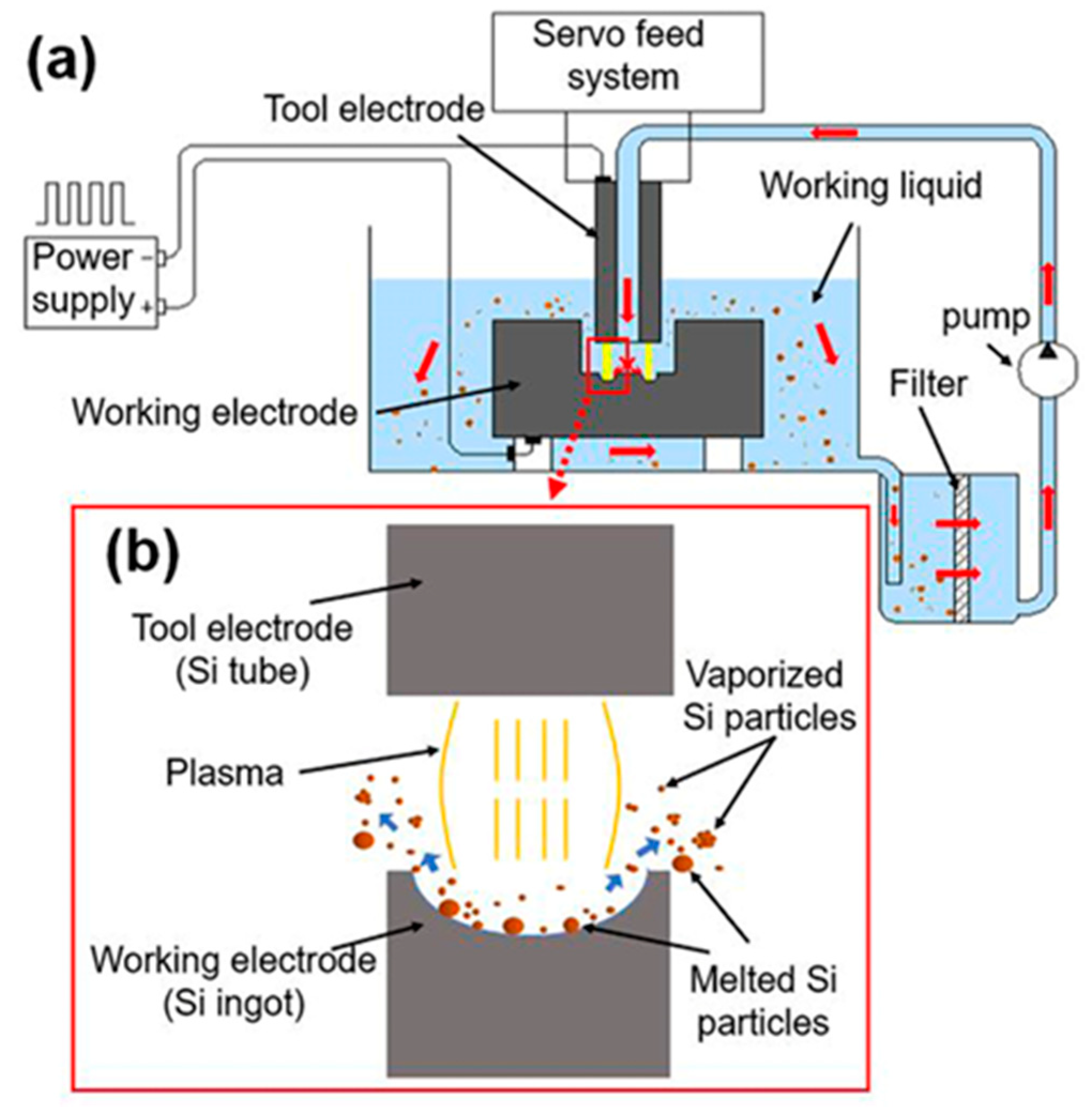
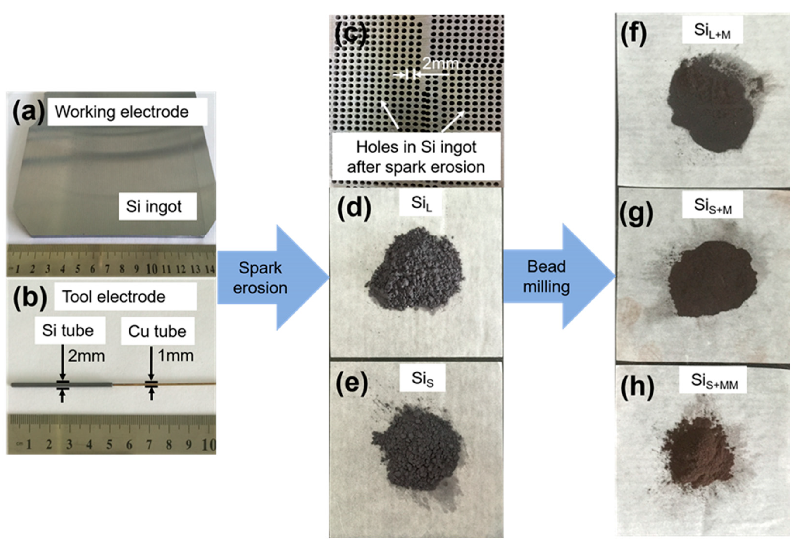
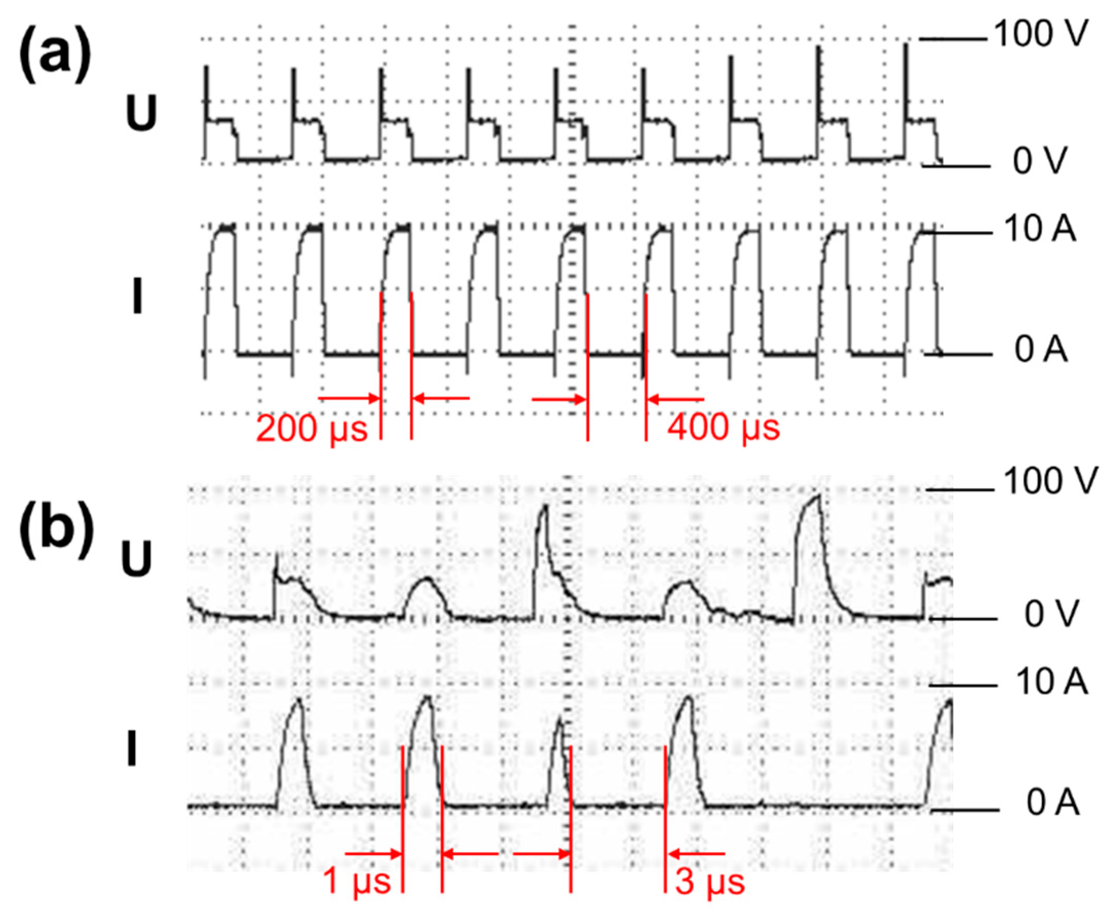
2.1. Spark Erosion
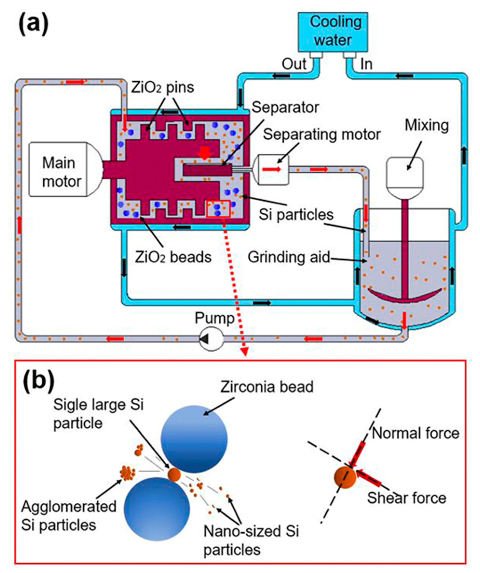
2.2. Bead Milling
2.3. Characterization
3. Results and Discussion
3.1. Particles Morphology
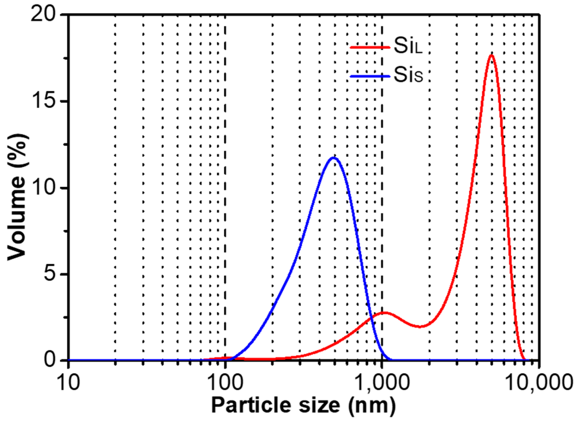
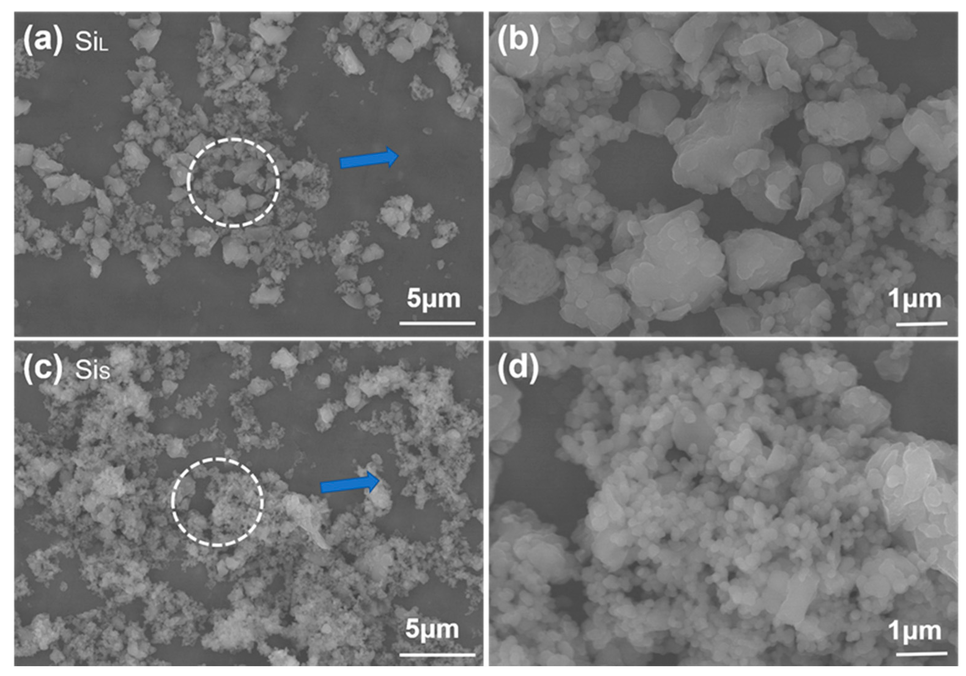
3.1.1. Morphology of Si Micro/Nano Particles Prepared by Spark Erosion
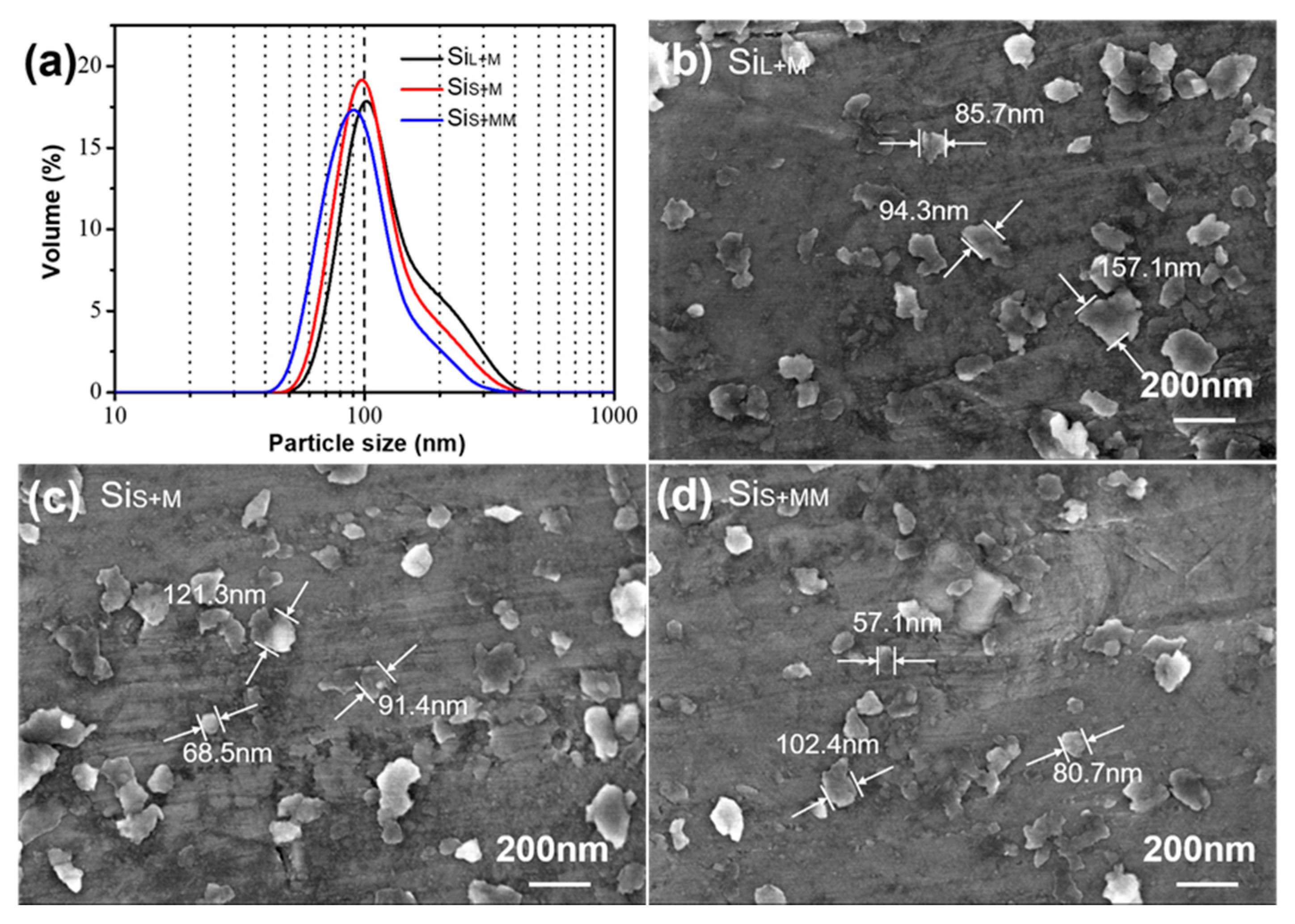
3.1.2. Morphology of Si Nanoparticles Prepared by Bead Milling
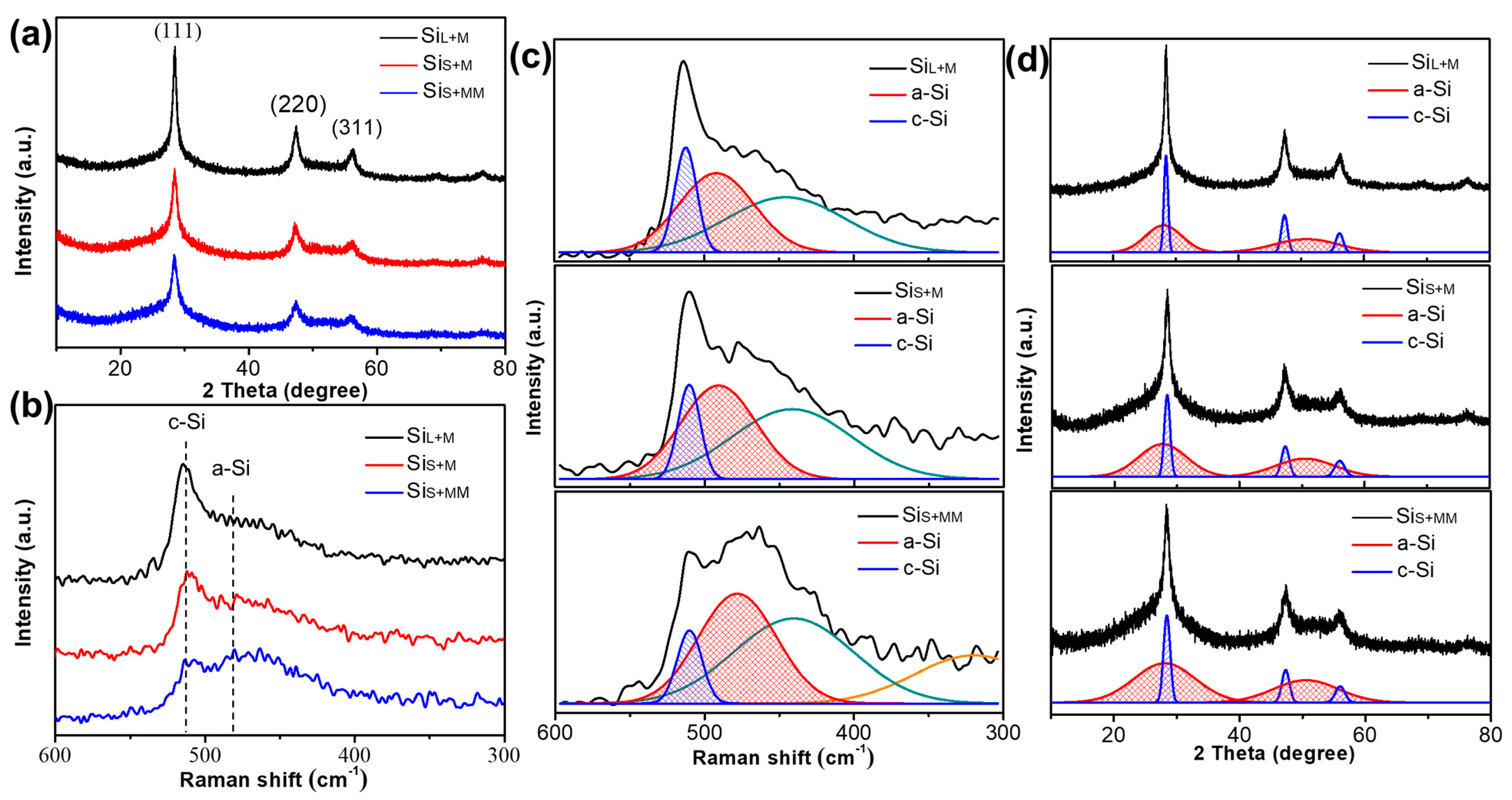
3.2. Internal Structure of Prepared Si Particles
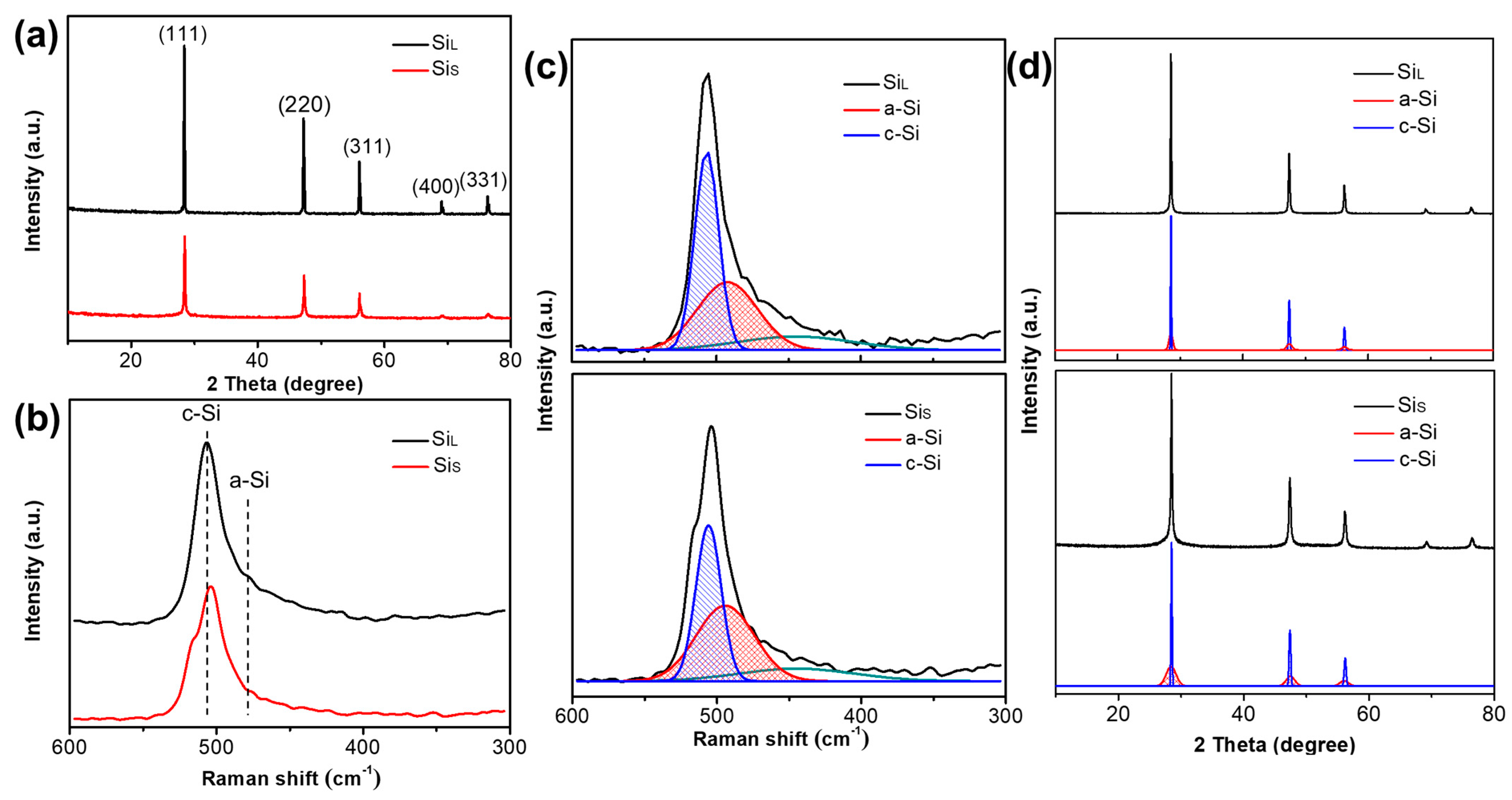
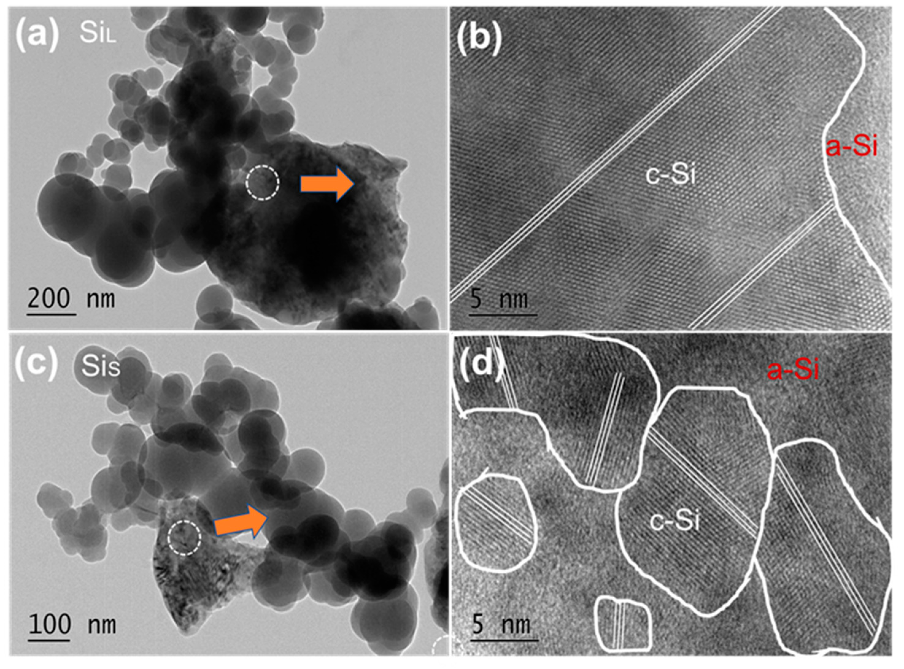
3.2.1. Internal Structure of Si Micro/Nano Particles Prepared by Spark Erosion
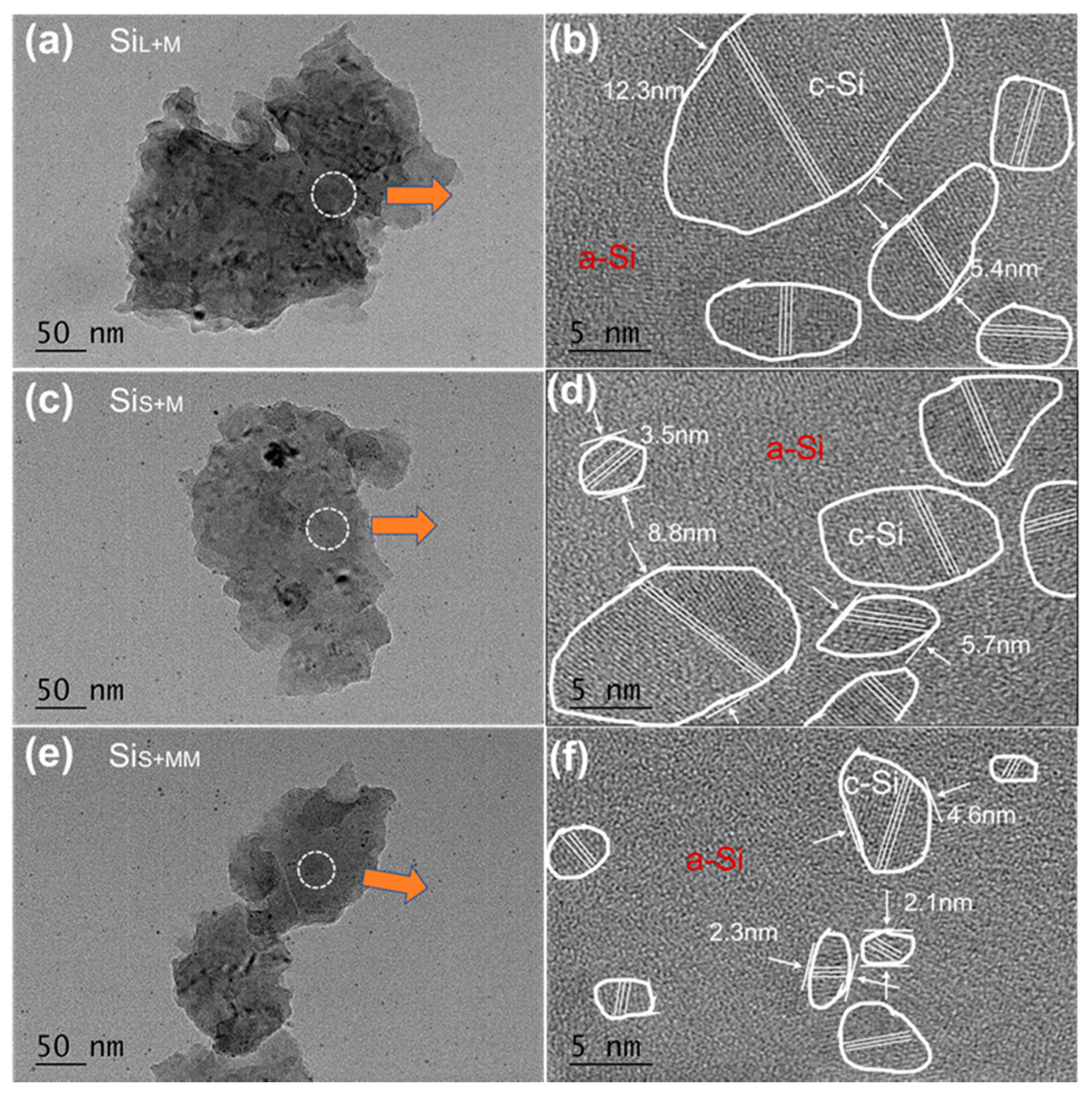
3.2.2. Internal Structure of Si Nanoparticles Prepared by Bead Milling
4. Conclusions
Author Contributions
Funding
Institutional Review Board Statement
Informed Consent Statement
Data Availability Statement
Acknowledgments
Conflicts of Interest
References
- Botas, A.M.P.; Leitão, J.P.; Falcao, B.P.; Wiesinger, M.; Eckmann, F.; Teixeira, J.P.; Wiggers, H.; Stutzmann, M.; Ferreira, R.A.S.; Pereira, R.N. Silicon Nanoparticle Films Infilled with Al2O3 Using Atomic Layer Deposition for Photosensor, Light Emission, and Photovoltaic Applications. ACS Appl. Nano Mater. 2020, 3, 5033–5044. [Google Scholar] [CrossRef]
- Erogbogbo, F.; Yong, K.-T.; Roy, I.; Xu, G.; Prasad, P.N.; Swihart, M.T. Biocompatible Luminescent Silicon Quantum Dots for Imaging of Cancer Cells. ACS Nano 2008, 2, 873–878. [Google Scholar] [CrossRef] [PubMed]
- Zhong, W. Nanomaterials in fluorescence-based biosensing. Anal. Bioanal. Chem. 2009, 394, 47–59. [Google Scholar] [CrossRef]
- Ye, Z.; Srivastava, P.K.; Xu, Y.; Wang, W.; Jing, L.; Chen, S.-L.; Tu, C.-C. Surface-Functionalized Silicon Nanoparticles as Contrast Agents for Photoacoustic Microscopy Imaging. ACS Appl. Nano Mater. 2019, 2, 7577–7584. [Google Scholar] [CrossRef]
- Hughes, G.A. Nanostructure-mediated drug delivery. Nanomedicine: Nanotechnology, Biol. Med. 2005, 1, 22–30. [Google Scholar] [CrossRef] [PubMed]
- Pi, X.; Li, Q.; Li, D.; Yang, D. Spin-coating silicon-quantum-dot ink to improve solar cell efficiency. Sol. Energy Mater. Sol. Cells 2011, 95, 2941–2945. [Google Scholar] [CrossRef]
- Fojtik, A.; Valenta, J.; Pelant, I.; Kalal, M.; Fiala, P. On the road to silicon-nanoparticle laser. J. Mater. Process. Technol. 2007, 181, 88–92. [Google Scholar] [CrossRef]
- Zhang, L.; Zhang, L.; Zhang, J.; Hao, W.; Zheng, H. Robust polymeric coating enables the stable operation of silicon micro-plate anodes recovered from photovoltaic industry waste for high-performance Li-ion batteries. J. Mater. Chem. A 2015, 3, 15432–15443. [Google Scholar] [CrossRef]
- Zhao, X.; Lehto, V.-P. Challenges and prospects of nanosized silicon anodes in lithium-ion batteries. Nanotechnol. 2021, 32, 042002. [Google Scholar] [CrossRef]
- Zhang, Y.; Ren, J.; Xu, T.; Feng, A.; Hu, K.; Yu, N.; Xia, Y.; Zhu, Y.; Huang, Z.; Wu, G. Covalent Bonding of Si Nanoparticles on Graphite Nanosheets as Anodes for Lithium-Ion Batteries Using Diazonium Chemistry. Nanomater. 2019, 9, 1741. [Google Scholar] [CrossRef]
- Wei, C.-Y.; Sun, Y.-T.; Liu, Y.-L.; Liu, T.-R.; Wen, C.-Y. Lithiation-induced fracture of silicon nanowires observed by in-situ scanning electron microscopy. Nanotechnol. 2020, 31, 364001. [Google Scholar] [CrossRef]
- Chan, C.K.; Peng, H.; Liu, G.; McIlwrath, K.; Zhang, X.F.; Huggins, R.A.; Cui, Y. High-performance lithium battery anodes using silicon nanowires. Nat. Nanotechnol. 2007, 3, 31–35. [Google Scholar] [CrossRef] [PubMed]
- Azib, T.; Thaury, C.; Cuevas, F.; Leroy, E.; Jordy, C.; Marx, N.; Latroche, M. Impact of Surface Chemistry of Silicon Nano-particles on the Structural and Electrochemical Properties of Si/Ni3.4Sn4 Composite Anode for Li-Ion Batteries. Nanomaterials 2021, 11, 18. [Google Scholar] [CrossRef]
- Deringer, V.L.; Bernstein, N.; Csányi, G.; Ben Mahmoud, C.; Ceriotti, M.; Wilson, M.; Drabold, D.A.; Elliott, S.R. Origins of structural and electronic transitions in disordered silicon. Nat. Cell Biol. 2021, 589, 59–64. [Google Scholar] [CrossRef]
- Yao, Y.; McDowell, M.T.; Ryu, I.; Wu, H.; Liu, N.; Hu, L.; Nix, W.D.; Cui, Y. Interconnected Silicon Hollow Nanospheres for Lithium-Ion Battery Anodes with Long Cycle Life. Nano Lett. 2011, 11, 2949–2954. [Google Scholar] [CrossRef]
- Cui, L.; Ruffo, R.; Chan, C.K.; Peng, H.; Cui, Y. Crystalline-Amorphous Core−Shell Silicon Nanowires for High Capacity and High Current Battery Electrodes. Nano Lett. 2009, 9, 491–495. [Google Scholar] [CrossRef]
- Liu, X.H.; Zhong, L.; Huang, S.; Mao, S.X.; Zhu, T.; Huang, J.Y. Size-Dependent Fracture of Silicon Nanoparticles During Lithiation. ACS Nano 2012, 6, 1522–1531. [Google Scholar] [CrossRef] [PubMed]
- McDowell, M.T.; Lee, S.W.; Harris, J.T.; Korgel, B.A.; Wang, C.; Nix, W.D.; Cui, Y. In Situ TEM of Two-Phase Lithiation of Amorphous Silicon Nanospheres. Nano Lett. 2013, 13, 758–764. [Google Scholar] [CrossRef] [PubMed]
- Leach, W.; Zhu, J.-H.; Ekerdt, J.G. Thermal desorption effects in chemical vapor deposition of silicon nanoparticles. J. Cryst. Growth 2002, 243, 30–40. [Google Scholar] [CrossRef]
- Mangolini, L.; Thimsen, E.; Kortshagen, U. High-Yield Plasma Synthesis of Luminescent Silicon Nanocrystals. Nano Lett. 2005, 5, 655–659. [Google Scholar] [CrossRef] [PubMed]
- Yu, Y.; Gu, L.; Zhu, C.; Tsukimoto, S.; Van Aken, P.A.; Maier, J. Reversible Storage of Lithium in Silver-Coated Three-Dimensional Macroporous Silicon. Adv. Mater. 2010, 22, 2247–2250. [Google Scholar] [CrossRef]
- Amoruso, S.; Bruzzese, R.; Spinelli, N.; Velotta, R.; Vitiello, M.; Wang, X.Q.; Ausanio, G.; Iannotti, V.; Lanotte, L. Generation of silicon nanoparticles via femtosecond laser ablation in vacuum. Appl. Phys. Lett. 2004, 84, 4502–4504. [Google Scholar] [CrossRef]
- Chao, Y.; Iller, L.S.; Krishnamurthy, S.; Coxon, P.R.; Bangert, U.; Gass, M.; Kjeldgaard, L.; Patole, S.N.; Lie, L.H.; O’Farrell, N.; et al. Evaporation and deposition of alkyl-capped silicon nanocrystals in ultrahigh vacuum. Nat. Nanotechnol. 2007, 2, 486–489. [Google Scholar] [CrossRef] [PubMed]
- Zhang, W.; Farooq, A.; Wang, W. Generating Silicon Nanoparticles Using Spark Erosion by Flushing High-Pressure Deionized Water. Mater. Manuf. Process. 2014, 31, 113–118. [Google Scholar] [CrossRef]
- Swihart, M.T. Vapor-phase synthesis of nanoparticles. Curr. Opin. Colloid Interface Sci. 2003, 8, 127–133. [Google Scholar] [CrossRef]
- Yekeler, M.; Ozkan, A.; Austin, L. Kinetics of fine wet grinding in a laboratory ball mill. Powder Technol. 2001, 114, 224–228. [Google Scholar] [CrossRef]
- Hou, S.-C.; Su, Y.-F.; Chang, C.-C.; Hu, C.-W.; Chen, T.-Y.; Yang, S.-M.; Huang, J.-L. The synergistic effects of combining the high energy mechanical milling and wet milling on Si negative electrode materials for lithium ion battery. J. Power Sources 2017, 349, 111–120. [Google Scholar] [CrossRef]
- Hou, X.; Zhang, M.; Wang, J.; Hu, S.; Liu, X.; Shao, Z. High yield and low-cost ball milling synthesis of nano-flake Si@SiO2 with small crystalline grains and abundant grain boundaries as a superior anode for Li-ion batteries. J. Alloy Compd. 2015, 639, 27–35. [Google Scholar] [CrossRef]
- Vons, V.A.; De Smet, L.C.P.M.; Munaò, D.; Evirgen, A.; Kelder, E.M.; Schmidt-Ott, A. Silicon nanoparticles produced by spark discharge. J. Nanoparticle Res. 2011, 13, 4867–4879. [Google Scholar] [CrossRef]
- Wong, Y.; Rahman, M.; Lim, H.; Han, H.; Ravi, N. Investigation of micro-EDM material removal characteristics using single RC-pulse discharges. J. Mater. Process. Technol. 2003, 140, 303–307. [Google Scholar] [CrossRef]
- Erden, A. Effect of Materials on the Mechanism of Electric Discharge Machining (E.D.M.). J. Eng. Mater. Technol. 1983, 105, 132–138. [Google Scholar] [CrossRef]
- Kwade, A. Determination of the most important grinding mechanism in stirred media mills by calculating stress intensity and stress number. Powder Technol. 1999, 105, 382–388. [Google Scholar] [CrossRef]
- Wang, Y.; Forssberg, E. Production of carbonate and silica nano-particles in stirred bead milling. Int. J. Miner. Process. 2006, 81, 1–14. [Google Scholar] [CrossRef]
- Lorusso, A.; Nassisi, V.; Congedo, G.; Lovergine, N.; Velardi, L.; Prete, P. Pulsed plasma ion source to create Si nanocrystals in SiO2 substrates. Appl. Surf. Sci. 2009, 255, 5401–5404. [Google Scholar] [CrossRef]
- Terada, S.; Xin, Y.; Saitow, K.-I. Cost-Effective Synthesis of Silicon Quantum Dots. Chem. Mater. 2020, 32, 8382–8392. [Google Scholar] [CrossRef]
- Zhigunov, D.M.; Kamaev, G.N.; Kashkarov, P.K.; Volodin, V.A. On Raman scattering cross section ratio of crystalline and microcrystalline to amorphous silicon. Appl. Phys. Lett. 2018, 113, 023101. [Google Scholar] [CrossRef]
- Yang, C.; Yao, Y.; He, S.; Xie, H.; Hitz, E.; Hu, L. Ultrafine Silver Nanoparticles for Seeded Lithium Deposition toward Stable Lithium Metal Anode. Adv. Mater. 2017, 29, 1702714. [Google Scholar] [CrossRef]
- Chipera, S.J.; Bish, D.L. FULLPAT: A full-pattern quantitative analysis program for X-ray powder diffraction using measured and calculated patterns. J. Appl. Crystallogr. 2002, 35, 744–749. [Google Scholar] [CrossRef]
- Tello, M.; García, R. Giant growth rate in nano-oxidation of p-silicon surfaces by using ethyl alcohol liquid bridges. Appl. Phys. Lett. 2003, 83, 2339. [Google Scholar] [CrossRef]
- Kim, N.Y.; Laibinis, P.E. Thermal Derivatization of Porous Silicon with Alcohols. J. Am. Chem. Soc. 1997, 119, 2297–2298. [Google Scholar] [CrossRef]
- Fujiwara, K.; Nakajima, K.; Ujihara, T.; Usami, N.; Sazaki, G.; Hasegawa, H.; Mizoguchi, S.; Nakajima, K. In situ observations of crystal growth behavior of silicon melt. J. Cryst. Growth 2002, 243, 275–282. [Google Scholar] [CrossRef]
- Wang, T.; Hsu, S.; Fei, C.; Yei, K.; Hsu, W.; Lan, C.-W. Grain control using spot cooling in multi-crystalline silicon crystal growth. J. Cryst. Growth 2009, 311, 263–267. [Google Scholar] [CrossRef]
- Fujiwara, K.; Obinata, Y.; Ujihara, T.; Usami, N.; Sazaki, G.; Nakajima, K. Grain growth behaviors of polycrystalline silicon during melt growth processes. J. Cryst. Growth 2004, 266, 441–448. [Google Scholar] [CrossRef]
- Delogu, F.; Cocco, G. Crystallite size refinement in elemental species under mechanical processing conditions. Mater. Sci. Eng. A 2006, 422, 198–204. [Google Scholar] [CrossRef]


| Parameters | SiL | SiS |
|---|---|---|
| Working electrode | Si ingot (10 mm thick) | |
| Tool electrode | Si hollow tube (50 mm long, the external and internal diameter is 2 mm and 1 mm, respectively) | |
| Working liquid | Deionized water (resistivity is 10 MΩ·cm−1) | |
| Open-circuit voltage(V) | 100 | 100 |
| Peak current (A) | 10 | 10 |
| Pulse duration (μs) | 200 | 1 |
| Duty cycle | 1:2 | 1:3 |
| Parameters | SiL+M | SiS+M | SiS+MM |
|---|---|---|---|
| Grinding aid | Ethyl alcohol (1800 g) | ||
| Beads | 0.1 mm, 2 kg (ZrO2, bulk density is 3.5 kg/L) | ||
| Effective volume of the bead milling equipment | 0.7 L (filling rate of beads is about 81.6%) | ||
| Linear velocity | 13.5 m/s (rotation speed is 2300 r/min) | ||
| Temperature of cooling water | <10 °C | ||
| Raw material | SiL (200 g) | SiS (200 g) | SiS (200 g) |
| Grinding time | 8 h | 8 h | 12 h |
| Samples | The Average Crystallite Size (nm) | Oxygen Content (%) | ||
|---|---|---|---|---|
| SiL | 68.92 | 31.8 | 27.8 | 1.3 |
| SiS | 26.47 | 47.5 | 46.3 | 2.5 |
| SiL+M | 11.73 | 69.4 | 70.4 | 5.8 |
| SiS+M | 6.18 | 74.8 | 75.6 | 6.2 |
| SiS+MM | 4.23 | 83.7 | 83.1 | 8.7 |
Publisher’s Note: MDPI stays neutral with regard to jurisdictional claims in published maps and institutional affiliations. |
© 2021 by the authors. Licensee MDPI, Basel, Switzerland. This article is an open access article distributed under the terms and conditions of the Creative Commons Attribution (CC BY) license (http://creativecommons.org/licenses/by/4.0/).
Share and Cite
Zhao, M.; Zhang, J.; Wang, W.; Zhang, Q. High Effective Preparation of Amorphous-Like Si Nanoparticles Using Spark Erosion Followed by Bead Milling. Nanomaterials 2021, 11, 594. https://doi.org/10.3390/nano11030594
Zhao M, Zhang J, Wang W, Zhang Q. High Effective Preparation of Amorphous-Like Si Nanoparticles Using Spark Erosion Followed by Bead Milling. Nanomaterials. 2021; 11(3):594. https://doi.org/10.3390/nano11030594
Chicago/Turabian StyleZhao, Mingcai, Juan Zhang, Wei Wang, and Qi Zhang. 2021. "High Effective Preparation of Amorphous-Like Si Nanoparticles Using Spark Erosion Followed by Bead Milling" Nanomaterials 11, no. 3: 594. https://doi.org/10.3390/nano11030594
APA StyleZhao, M., Zhang, J., Wang, W., & Zhang, Q. (2021). High Effective Preparation of Amorphous-Like Si Nanoparticles Using Spark Erosion Followed by Bead Milling. Nanomaterials, 11(3), 594. https://doi.org/10.3390/nano11030594