
Band Structure and Energy Level Alignment of Chiral Graphene Nanoribbons on Silver Surfaces

 , , , and
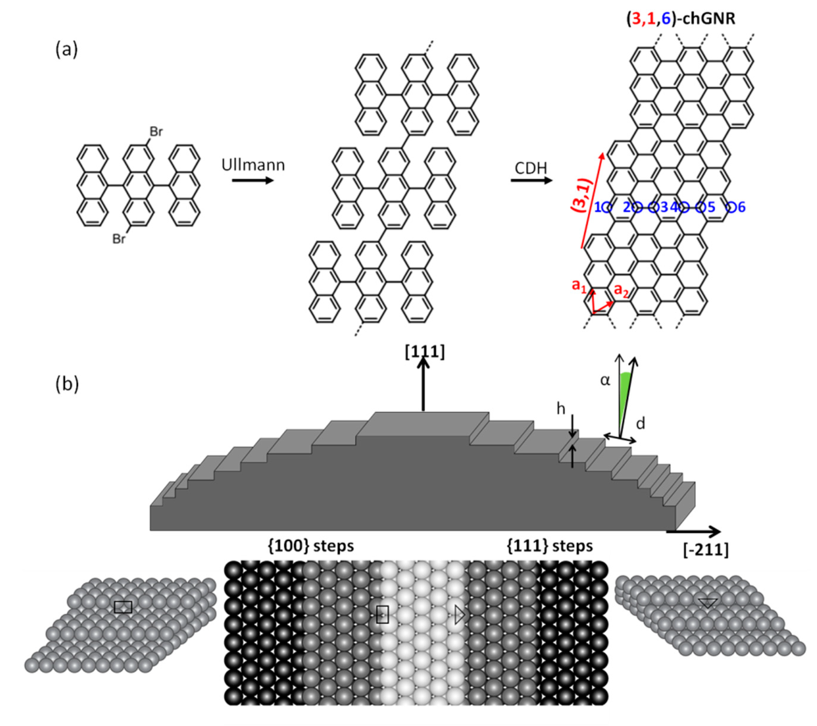
Abstract
:1. Introduction
2. Materials and Methods
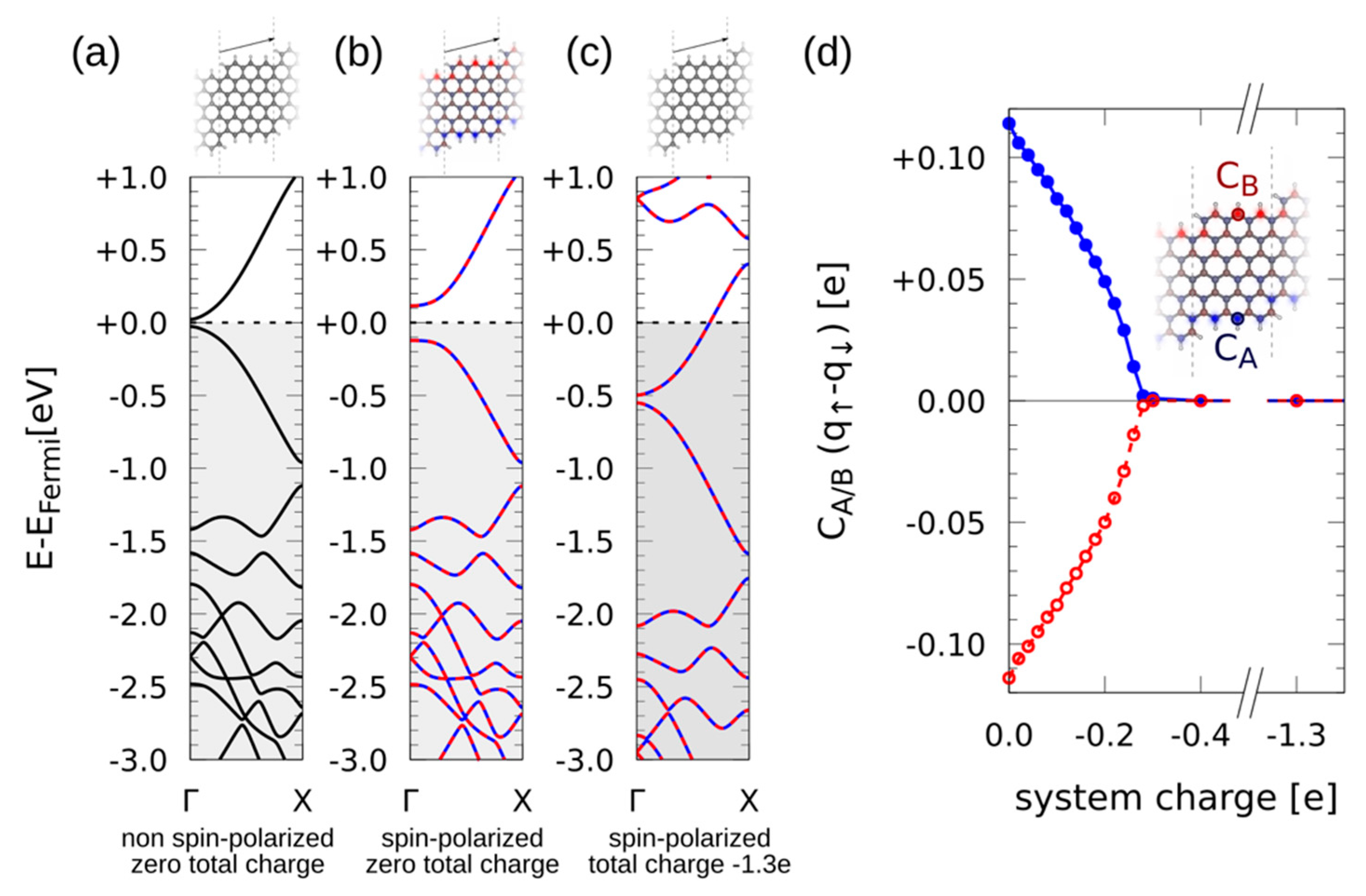
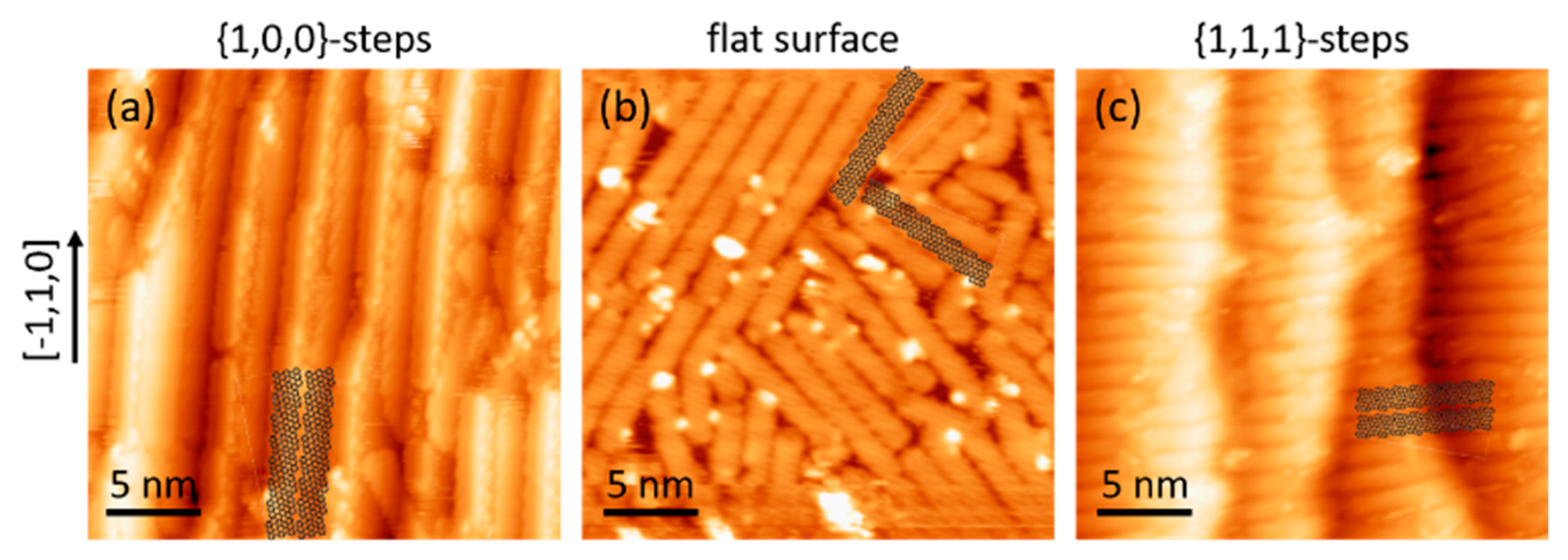
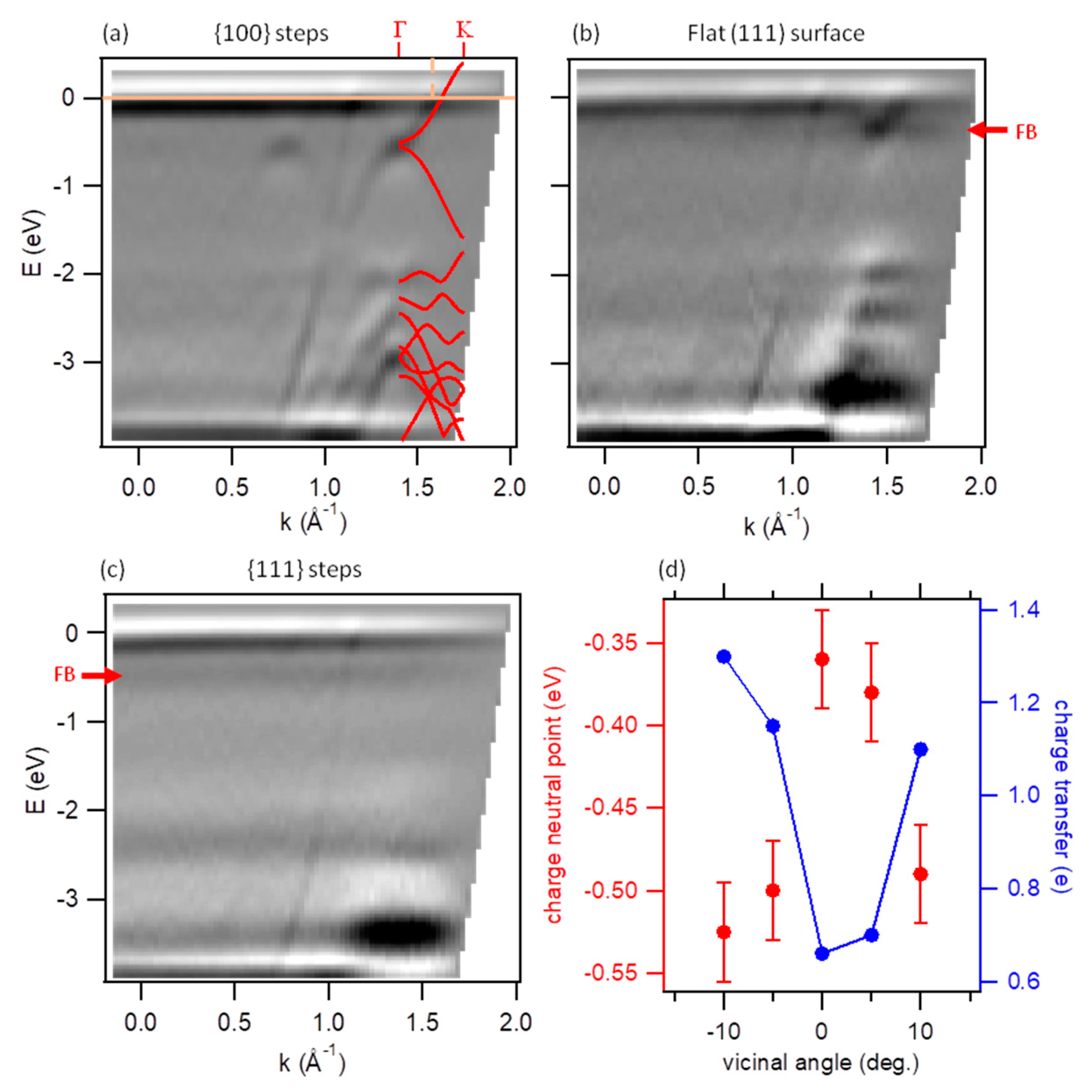
3. Results
4. Discussion
5. Conclusions
Supplementary Materials
Author Contributions
Funding
Data Availability Statement
Conflicts of Interest
References
- Wakabayashi, K.; Sasaki, K.; Nakanishi, T.; Enoki, T. Electronic States of Graphene Nanoribbons and Analytical Solutions. Sci. Technol. Adv. Mater. 2010, 11, 054504. [Google Scholar] [CrossRef] [PubMed] [Green Version]
- Corso, M.; Carbonell-Sanromà, E.; de Oteyza, D.G. Bottom-up Fabrication of Atomically Precise Graphene Nanoribbons. In On-Surface Synthesis II: Advances in Atom and Single Molecule Machines; Springer: Cham, Switzerland, 2018; pp. 113–152. [Google Scholar]
- Yano, Y.; Mitoma, N.; Ito, H.; Itami, K. A Quest for Structurally Uniform Graphene Nanoribbons: Synthesis, Properties, and Applications. J. Org. Chem. 2020, 85, 4–33. [Google Scholar] [CrossRef]
- Yazyev, O.V.; Capaz, R.B.; Louie, S.G. Theory of Magnetic Edge States in Chiral Graphene Nanoribbons. Phys. Rev. B 2011, 84, 115406. [Google Scholar] [CrossRef] [Green Version]
- Yazyev, O.V. Emergence of Magnetism in Graphene Materials and Nanostructures. Rep. Prog. Phys. 2010, 73, 056501. [Google Scholar] [CrossRef]
- Suda, S.; Oshiyama, A. Energetics, Electron States, and Magnetization in Nearly Zigzag-Edged Graphene Nano-Ribbons. J. Phys. Soc. Jpn. 2015, 84, 024704. [Google Scholar] [CrossRef]
- Merino-Díez, N.; Li, J.; Garcia-Lekue, A.; Vasseur, G.; Vilas-Varela, M.; Carbonell-Sanromà, E.; Corso, M.; Ortega, J.E.; Peña, D.; Pascual, J.I.; et al. Unraveling the Electronic Structure of Narrow Atomically-Precise Chiral Graphene Nanoribbons. J. Phys. Chem. Lett. 2018, 9, 25–30. [Google Scholar] [CrossRef] [Green Version]
- Li, J.; Sanz, S.; Merino-Díez, N.; Vilas-Varela, M.; Garcia-Lekue, A.; Corso, M.; de Oteyza, D.G.; Frederiksen, T.; Peña, D.; Pascual, J.I. Topological Phase Transition in Chiral Graphene Nanoribbons: From Edge Bands to End States. Nat. Commun. 2021, 12, 5538. [Google Scholar] [CrossRef]
- Ruffieux, P.; Wang, S.; Yang, B.; Sánchez-Sánchez, C.; Liu, J.; Dienel, T.; Talirz, L.; Shinde, P.; Pignedoli, C.A.; Passerone, D.; et al. On-Surface Synthesis of Graphene Nanoribbons with Zigzag Edge Topology. Nature 2016, 531, 489–492. [Google Scholar] [CrossRef] [Green Version]
- Gröning, O.; Wang, S.; Yao, X.; Pignedoli, C.A.; Borin Barin, G.; Daniels, C.; Cupo, A.; Meunier, V.; Feng, X.; Narita, A.; et al. Engineering of Robust Topological Quantum Phases in Graphene Nanoribbons. Nature 2018, 560, 209–213. [Google Scholar] [CrossRef] [PubMed] [Green Version]
- Rizzo, D.J.; Veber, G.; Cao, T.; Bronner, C.; Chen, T.; Zhao, F.; Rodriguez, H.; Louie, S.G.; Crommie, M.F.; Fischer, F.R. Topological Band Engineering of Graphene Nanoribbons. Nature 2018, 560, 204–208. [Google Scholar] [CrossRef]
- Rizzo, D.J.; Veber, G.; Jingwei, J.; McCurdy, R.; Cao, T.; Bronner, C.; Chen, T.; Louie, S.G.; Fischer, F.R.; Crommie, M.F. Inducing Metallicity in Graphene Nanoribbonsvia Zero-Mode Superlattices. Science 2020, 369, 1597–1603. [Google Scholar] [CrossRef]
- Ortega, J.E.; Corso, M.; Abd-el-Fattah, Z.M.; Goiri, E.A.; Schiller, F. Interplay between Structure and Electronic States in Step Arrays Explored with Curved Surfaces. Phys. Rev. B 2011, 83, 085411. [Google Scholar] [CrossRef] [Green Version]
- Horcas, I.; Fernández, R.; Gómez-Rodríguez, J.M.; Colchero, J.; Gómez-Herrero, J.; Baro, A.M. WSXM: A Software for Scanning Probe Microscopy and a Tool for Nanotechnology. Rev. Sci. Instrum. 2007, 78, 013705. [Google Scholar] [CrossRef] [PubMed]
- Artacho, E.; Sánchez-Portal, D.; Ordejón, P.; García, A.; Soler, J.M. Linear-Scaling Ab-Initio Calculations for Large and Complex Systems. Phys. Status Solidi B 1999, 215, 809–817. [Google Scholar] [CrossRef] [Green Version]
- Soler, J.M.; Artacho, E.; Gale, J.D.; García, A.; Junquera, J.; Ordejón, P.; Sánchez-Portal, D. The SIESTA Method for Ab Initio Order- N Materials Simulation. J. Phys. Condens. Matter 2002, 14, 2745–2779. [Google Scholar] [CrossRef] [Green Version]
- Dion, M.; Rydberg, H.; Schröder, E.; Langreth, D.C.; Lundqvist, B.I. Van Der Waals Density Functional for General Geometries. Phys. Rev. Lett. 2004, 92, 246401. [Google Scholar] [CrossRef] [PubMed] [Green Version]
- Klimeš, J.; Bowler, D.R.; Michaelides, A. Chemical Accuracy for the van Der Waals Density Functional. J. Phys. Condens. Matter 2010, 22, 022201. [Google Scholar] [CrossRef]
- Troullier, N.; Martins, J.L. Efficient Pseudopotentials for Plane-Wave Calculations. Phys. Rev. B 1991, 43, 1993–2006. [Google Scholar] [CrossRef] [PubMed]
- Ruffieux, P.; Cai, J.; Plumb, N.C.; Patthey, L.; Prezzi, D.; Ferretti, A.; Molinari, E.; Feng, X.; Müllen, K.; Pignedoli, C.A.; et al. Electronic Structure of Atomically Precise Graphene Nanoribbons. ACS Nano 2012, 6, 6930–6935. [Google Scholar] [CrossRef]
- Passi, V.; Gahoi, A.; Senkovskiy, B.V.; Haberer, D.; Fischer, F.R.; Grüneis, A.; Lemme, M.C. Field-Effect Transistors Based on Networks of Highly Aligned, Chemically Synthesized N = 7 Armchair Graphene Nanoribbons. ACS Appl. Mater. Interfaces 2018, 10, 9900–9903. [Google Scholar] [CrossRef] [PubMed]
- Merino-Díez, N.; Lobo-Checa, J.; Nita, P.; Garcia-Lekue, A.; Basagni, A.; Vasseur, G.; Tiso, F.; Sedona, F.; Das, P.K.; Fujii, J.; et al. Switching from Reactant to Substrate Engineering in the Selective Synthesis of Graphene Nanoribbons. J. Phys. Chem. Lett. 2018, 9, 2510–2517. [Google Scholar] [CrossRef] [PubMed] [Green Version]
- Piquero-Zulaica, I.; Garcia-Lekue, A.; Colazzo, L.; Krug, C.K.; Mohammed, M.S.G.; Abd El-Fattah, Z.M.; Gottfried, J.M.; de Oteyza, D.G.; Ortega, J.E.; Lobo-Checa, J. Electronic Structure Tunability by Periodic Meta-Ligand Spacing in One-Dimensional Organic Semiconductors. ACS Nano 2018, 12, 10537–10544. [Google Scholar] [CrossRef] [PubMed] [Green Version]
- El-Sayed, A.; Piquero-Zulaica, I.; Abd El-Fattah, Z.M.; Kormoš, L.; Ali, K.; Weber, A.; Brede, J.; de Oteyza, D.G.; Lobo-Checa, J.; Ortega, J.E.; et al. Synthesis of Graphene Nanoribbons on a Kinked Au Surface: Revealing the Frontier Valence Band at the Brillouin Zone Center. J. Phys. Chem. C 2020, 124, 15474–15480. [Google Scholar] [CrossRef]
- Ma, C.; Xiao, Z.; Lu, W.; Huang, J.; Hong, K.; Bernholc, J.; Li, A.-P. Step Edge-Mediated Assembly of Periodic Arrays of Long Graphene Nanoribbons on Au(111). Chem. Commun. 2019, 55, 11848–11851. [Google Scholar] [CrossRef] [PubMed]
- Merino-Díez, N.; Garcia-Lekue, A.; Carbonell-Sanromà, E.; Li, J.; Corso, M.; Colazzo, L.; Sedona, F.; Sánchez-Portal, D.; Pascual, J.I.; de Oteyza, D.G. Width-Dependent Band Gap in Armchair Graphene Nanoribbons Reveals Fermi Level Pinning on Au(111). ACS Nano 2017, 11, 11661–11668. [Google Scholar] [CrossRef]
- Uda, M.; Nakamura, A.; Yamamoto, T.; Fujimoto, Y. Work Function of Polycrystalline Ag, Au and Al. J. Electron Spectrosc. Relat. Phenom. 1998, 88–91, 643–648. [Google Scholar] [CrossRef]
- Abadia, M.; Brede, J.; Verdini, A.; Floreano, L.; Nita, P.; de Oteyza, D.G.; Ortega, J.E.; Corso, M.; Rogero, C. Why a Good Catalyst Can Turn Out Detrimental to Good Polymerization. J. Phys. Chem. C 2021, 125, 5066–5075. [Google Scholar] [CrossRef]
- Goiri, E.; Borghetti, P.; El-Sayed, A.; Ortega, J.E.; de Oteyza, D.G. Multi-Component Organic Layers on Metal Substrates. Adv. Mater. 2016, 28, 1340–1368. [Google Scholar] [CrossRef]
- Borghetti, P.; El-Sayed, A.; Goiri, E.; Rogero, C.; Lobo-Checa, J.; Floreano, L.; Ortega, J.E.; de Oteyza, D.G. Spectroscopic Fingerprints of Work-Function-Controlled Phthalocyanine Charging on Metal Surfaces. ACS Nano 2014, 8, 12786–12795. [Google Scholar] [CrossRef] [PubMed] [Green Version]
- Carvalho, A.R.; Warnes, J.H.; Lewenkopf, C.H. Edge Magnetization and Local Density of States in Chiral Graphene Nanoribbons. Phys. Rev. B 2014, 89, 245444. [Google Scholar] [CrossRef] [Green Version]
- Dutta, S.; Wakabayashi, K. Tuning Charge and Spin Excitations in Zigzag Edge Nanographene Ribbons. Sci. Rep. 2012, 2, 519. [Google Scholar] [CrossRef] [PubMed] [Green Version]


Publisher’s Note: MDPI stays neutral with regard to jurisdictional claims in published maps and institutional affiliations. |
© 2021 by the authors. Licensee MDPI, Basel, Switzerland. This article is an open access article distributed under the terms and conditions of the Creative Commons Attribution (CC BY) license (https://creativecommons.org/licenses/by/4.0/).
Share and Cite
Corso, M.; Menchón, R.E.; Piquero-Zulaica, I.; Vilas-Varela, M.; Ortega, J.E.; Peña, D.; Garcia-Lekue, A.; de Oteyza, D.G. Band Structure and Energy Level Alignment of Chiral Graphene Nanoribbons on Silver Surfaces. Nanomaterials 2021, 11, 3303. https://doi.org/10.3390/nano11123303
Corso M, Menchón RE, Piquero-Zulaica I, Vilas-Varela M, Ortega JE, Peña D, Garcia-Lekue A, de Oteyza DG. Band Structure and Energy Level Alignment of Chiral Graphene Nanoribbons on Silver Surfaces. Nanomaterials. 2021; 11(12):3303. https://doi.org/10.3390/nano11123303
Chicago/Turabian StyleCorso, Martina, Rodrigo E. Menchón, Ignacio Piquero-Zulaica, Manuel Vilas-Varela, J. Enrique Ortega, Diego Peña, Aran Garcia-Lekue, and Dimas G. de Oteyza. 2021. "Band Structure and Energy Level Alignment of Chiral Graphene Nanoribbons on Silver Surfaces" Nanomaterials 11, no. 12: 3303. https://doi.org/10.3390/nano11123303
APA StyleCorso, M., Menchón, R. E., Piquero-Zulaica, I., Vilas-Varela, M., Ortega, J. E., Peña, D., Garcia-Lekue, A., & de Oteyza, D. G. (2021). Band Structure and Energy Level Alignment of Chiral Graphene Nanoribbons on Silver Surfaces. Nanomaterials, 11(12), 3303. https://doi.org/10.3390/nano11123303