Article

Narrow-Linewidth GaN-on-Si Laser Diode with Slot Gratings

1
School of Nano-Tech and Nano-Bionics, University of Science and Technology of China, Hefei 230026, China
2
Key Laboratory of Nanodevices and Applications, Suzhou Institute of Nano-Tech and Nano-Bionics (SINANO), Chinese Academy of Sciences (CAS), Suzhou 215123, China
3
Guangdong (Foshan) Branch, SINANO, CAS, Foshan 528000, China
4
Vacuum Interconnected Nanotech Workstation, SINANO, CAS, Suzhou 215123, China
*
Authors to whom correspondence should be addressed.
Nanomaterials 2021, 11(11), 3092; https://doi.org/10.3390/nano11113092
Submission received: 1 October 2021 / Revised: 5 November 2021 / Accepted: 12 November 2021 / Published: 16 November 2021
(This article belongs to the Special Issue State-of-the-Art Nanophotonics Materials and Devices in China)

Abstract

:
This letter reports room-temperature electrically pumped narrow-linewidth GaN-on-Si laser diodes. Unlike conventional distributed Bragg feedback laser diodes with hundreds of gratings, we employed only a few precisely defined slot gratings to narrow the linewidth and mitigate the negative effects of grating fabrication on the device performance. The slot gratings were incorporated into the ridge of conventional Fabry-Pérot cavity laser diodes. A subsequent wet etching in a tetramethyl ammonium hydroxide solution not only effectively removed the damages induced by the dry etching, but also converted the rough and tilted slot sidewalls into smooth and vertical ones. As a result, the threshold current was reduced by over 20%, and the reverse leakage current was decreased by over three orders of magnitude. Therefore, the room-temperature electrically pumped narrow-linewidth GaN-on-Si laser diode has been successfully demonstrated.

1. Introduction

Si photonics have been widely deemed as one of the leading technology paths for meeting the demand for a rapidly increasing data transfer rate, owing to the advantages of a large bandwidth, high speed and low power consumption [1,2,3,4,5]. However, the indirect bandgap nature of Si prohibits an efficient light emission [6,7]. Alternatively, direct-bandgap III-nitride semiconductors with a wide emission wavelength ranging from ultraviolet to infrared are the ideal materials for light-emitting diodes and laser diodes (LDs) [8,9,10]. Compared with conventional Fabry-Pérot (F-P) cavity LDs, narrow-linewidth LDs featured with precise wavelength tuning and high-speed modulation are more promising for optical interconnection [11]. Therefore, narrow-linewidth GaN-based LDs grown on Si could be utilized as a potential on-chip light source for Si photonics with III-nitride waveguides [12,13,14]. Moreover, narrow-linewidth GaN-based LDs also have emerging applications in atomic clocks, underwater communication, visible light communication, sensing, and master oscillator power amplifier systems [15,16,17,18,19,20,21].
The fabrication of narrow-linewidth GaN-based LDs faces multiple challenges. First of all, in order to narrow the lasing spectra, more than 100 pairs of Bragg gratings are often incorporated into conventional GaN-based F-P LDs [22,23,24]. Due to the chemical inertness of GaN, such Bragg gratings are usually fabricated by dry etching [25,26]. The sidewalls of the grating often suffer from roughness, poor steepness, and etching damage due to mask deformation, limitation of the aspect ratio, and high energy ion bombardment during the dry etching [27,28,29]. This would result in a large optical loss and low internal quantum efficiency owing to the light scattering and surface nonradiative recombination. Consequently, the threshold current of GaN-based narrow-linewidth LDs increased substantially, even by more than twice after the fabrication of Bragg gratings [30,31]. In addition, compared with that of GaAs or InP-based infrared lasers, the shorter emission wavelengths in GaN-based visible-light and ultraviolet LDs require smaller grating periods, generally in the sub-micrometer range. Therefore, the precise fabrication of such grating structures for GaN-based narrow-linewidth LDs is more challenging.
In this study, we report room-temperature electrically pumped narrow-linewidth GaN-on-Si LDs by mitigating the negative effects of slot etching. Only a few rationally designed slot gratings were introduced into the ridge of conventional F-P LDs to narrow the linewidth. A wet chemical treatment in a tetramethyl ammonium hydroxide (TMAH) solution effectively eliminated the damages caused by the dry etching, reducing the optical loss and electrical shunting. As a result, substantial reductions in the threshold current and leakage current were clearly observed.

2. Experimental Section

The slot and spacing are defined by Wsl = (2i + 1)λ0/4nsl and Wsp = (2j + 1)λ0/4nsp, respectively, where i and j are integers, and nsl and nsp are the effective refractive indexes of the slot region and the spacing region, respectively. λ0 is the Bragg wavelength and set to be the lasing wavelength of GaN-on-Si F-P LD [32]. The Bragg equation can be expressed as 2(nslWsl + nspWsp) = 0, where m is the order of the Bragg grating. The nsl and nsp were 2.455 and 2.523, calculated by the finite difference beam propagation method. It is worth noting that while the slot width is much larger than the lasing wavelength, the light scattering loss would be largely increased due to optical diffraction [32,33]. As a compromise between the lasing wavelength (~410 nm) and the aspect ratio limitation of focused ion beam (FIB) technology, the slot width Wsl was fixed as 380 nm to reduce light scattering loss, together with a spacing width (Wsp) of 1680 nm.
GaN-based laser material was epitaxially grown on an Si substrate by metalorganic chemical vapor deposition. Trimethylgallium, trimethylaluminum, trimethylindium and ammonia were used as precursors for gallium, aluminum, indium and nitrogen, respectively. The carrier gases are nitrogen and hydrogen. Monosilane and bisethylcyclopentadienylmagnesium were used as n- and p-type dopants, respectively. To eliminate the negative effect caused by the mismatch in both the lattice constant and coefficient of thermal expansion and condensed phases containing Si-basis [34,35], a carefully engineered AlN/AlGaN multilayer buffer was grown, and hence high-quality epitaxial GaN-on-Si templates could be obtained. On these templates, the laser structure consisted of an n-type GaN contact layer, an n-type Al0.07Ga0.93N cladding layer (CL), three pairs of In0.12Ga0.88N/In0.02Ga0.98N quantum wells (QWs) sandwiched by In0.01Ga0.99N waveguide layers (WG), an Al0.2Ga0.8N electron blocking layer (EBL), a p-type Al0.075Ga0.925N CL and a p-type GaN contact layer. More detailed laser structure information could be found in our previous work [36,37]. The as-grown laser epitaxial wafer was fabricated into edge-emitting F-P LDs with a ridge size of 4 × 800 μm2, and the cavity facets were formed by cleavage and left uncoated. Due to the highly resistive AlN/AlGaN buffer layer, a mesa was usually fabricated by dry etching to expose the n-GaN contact layer and form an n-type ohmic contact. Finally, a coplanar structure with both p- and n-contact pads on the same side was fabricated, as shown in Figure 1.
Subsequently, the slot gratings were formed in the ridge of the as-fabricated F-P LDs by FIB to narrow the linewidth, as shown in Figure 1a. Afterwards, the slotted F-P lasers were soaked in a 25% TMAH solution at 85 °C to remove the etching damages and steepen the sidewalls, and then an FIB etching together with scanning electron microscopy (SEM) measurement were used to track the slot morphology evolution. Before the FIB etching for the SEM observation, a layer of carbon was deposited on the slot surface to enhance the imaging contrast, and then a layer of platinum was also deposited to protect the surface from bombardment by a high energy ion beam.
Six slots divided the 800-μm long cavity into four sub-cavities with a length of 403, 120, 130 and 140 μm, respectively. The 403-μm long sub-cavity was mainly used to provide enough optical gain, and three shorter sub-cavities on both sides served as coupled cavities to select the optical mode based on the Vernier tuning mechanism [38,39,40]. From the viewpoint of optical coupling, it is preferable to fabricate slots through the QW to maximize the overlap between the optical field and slots. However, dry etching through the active region would significantly deteriorate the internal quantum efficiency. Therefore, the slots were etched with a depth of about 700 nm from the top p-GaN contact layer, and stopped at about 50 nm above the active region. The detailed information of the slotted F-P LD can be found in Figure 1b.
All the characterizations of GaN-on-Si LDs were performed at room temperature. The current-voltage (I-V) characteristic was measured by a continuous-wave power supply (Keithley 2400, Keithley, OH, USA), while the optoelectronic characteristics were tested under pulsed current injections with a 0.4% duty cycle and a 400 ns pulse width. The light output power as a function of the injection current (L-I) was measured by a calibrated optical power meter (PM121D, Thorlabs Inc., Newton, MA, USA). The electroluminescence (EL) spectra were collected by a high-resolution spectrometer (HORIBA 1250M, Horiba, Kyoto, Japan) with a resolution of approximately 6 pm. The morphologies of the slots and cavity facets were observed by SEM.

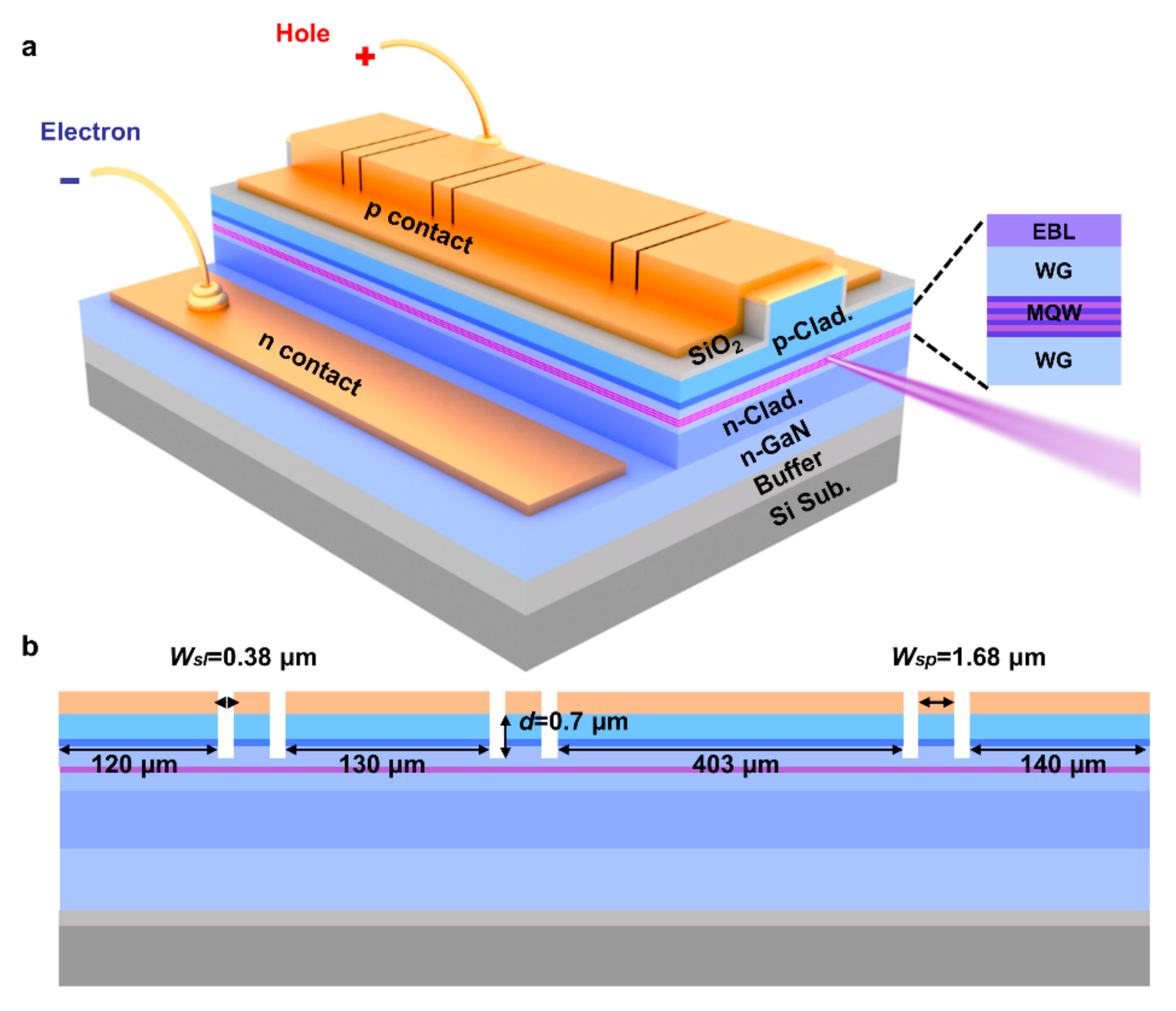
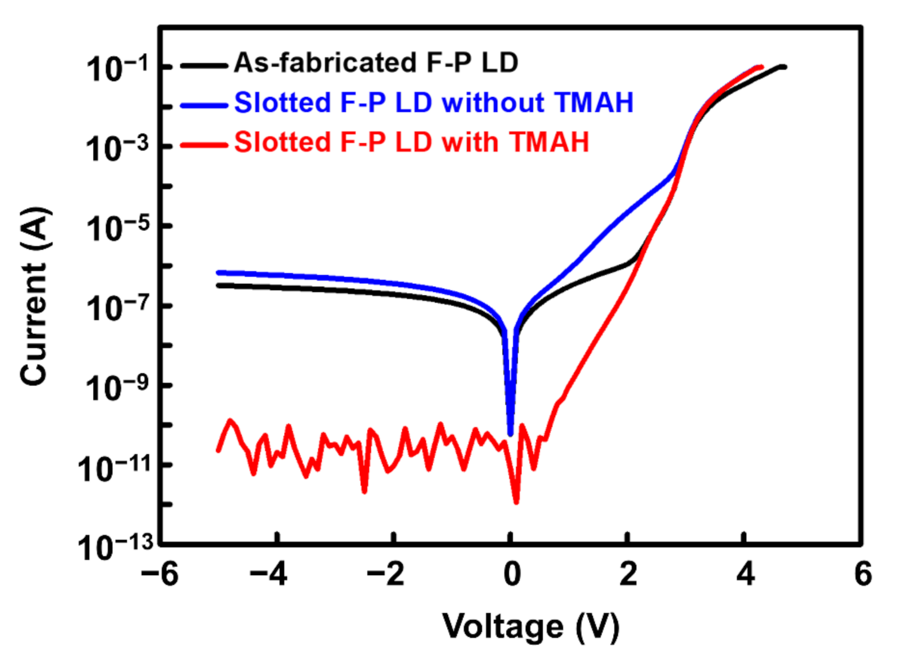
3. Results and Discussion

Figure 2a shows the change in the L-I curve of the LD during the process flow. The threshold current was 375 mA for the as-fabricated F-P LD before etching slots and increased to 415 mA after the slot fabrication. The slightly increased (~11%) threshold current of the slotted lasers validated the efficacy of the rationally selected grating parameters, in stark contrast to the drastic increase of the threshold current reported in the literature [30,31]. In addition, the optical power of the slotted F-P LD (12.8 mW) decreased slightly when compared with the as-fabricated F-P LD (15.2 mW) at the injection current of 430 mA. This reduction in optical power after fabricating gratings is much less than that reported by other studies [30,31]. The superior device performance of the slotted F-P LDs was elucidated through two aspects. First, hundreds or thousands of gratings were usually adopted in the reported narrow-linewidth LDs to select the single longitudinal mode, and these gratings were often fabricated by dry etching, resulting in a large optical loss and low internal quantum efficiency [23,31]. However, for slotted F-P LDs, only several slot gratings were fabricated, which significantly reduced the etching damages. Second, by restricting the slots above the active region, we not only reduced the etching damage to the active region but also enabled a relatively uniform current injection across the slots, as the lateral diffusion length of holes is larger than half of the slot width [41,42]. Subsequently, we employed TMAH post-treatment to remove the dry-etching damages, reducing the threshold current of the slotted F-P LD from 415 to 340 mA, as shown in Figure 2a.
Figure 2b shows the EL spectra of the as-fabricated F-P LD and slotted F-P LD. The EL spectra of the slotted F-P laser under various injection currents can also be found in Supplementary Figure S1. Many longitudinal modes were clearly observed for the as-fabricated F-P LD with a side-mode suppression ratio (SMSR) of 0.16 dB, and the mode spacing was ~38 pm, corresponding to a cavity length of 800 μm. The full width at half maximum (FWHM) of the spectrum was more than 1 nm. In contrast, for the slotted F-P LD, only one dominant emission peak with an FWHM of 25 pm as well as several effectively suppressed longitudinal modes were observed. The FWHM is similar to that of distributed feedback lasers reported by other literature [25,30]. In Figure 2c, it is indicated that the SMSR was as high as 13 dB, which is comparable with the results reported in the literature [23,43]. The mode spacing was also increased to 180 pm, which was 4.7 times that of the conventional F-P LD. The peak wavelength of the slotted F-P LD was 409.4 nm and blue-shifted from that of the as-fabricated F-P LD (412.1 nm), which was mainly due to the mismatch between the Bragg wavelength and lasing wavelength. The far-field patterns of the slotted F-P LD at the injection current below and above the threshold current are presented in Figure 2d,e, respectively. Above the threshold current, a typical elliptical far-field pattern was clearly observed. The slotted structure only influences the longitudinal modes and has little effect on the transverse mode distribution. Therefore, the far-field pattern divergence angles should be similar to that of the as-fabricated GaN-on-Si F-P LD with the same epitaxial and ridge structure. The typical far-filed pattern divergence angles of GaN-on-Si F-P can be found in our previous work [36]. These results, together with the lasing spectrum and typical L-I curve, demonstrated the unambiguous electrically pumped lasing of the slotted F-P LD at room temperature.
In order to investigate the effect of slot fabrication on the electrical properties of the LD, the I-V characteristics of as-fabricated F-P LD and slotted F-P with/without TMAH treatment were measured, as presented in Figure 3. It can be seen that after the slot fabrication in the ridge, the reverse leakage current was slightly increased from 3.2 × 10⁻⁷ to 6.7 × 10⁻⁷ A at a reverse bias of −5 V due to the etching damage, and the forward leakage current was also increased but was still very small when compared with the operation current. However, after the TMAH wet chemical etching, both the forward and reverse leakage currents of the slotted LDs were significantly decreased. In particular, the reverse leakage current was even reduced down to the measurement limitation of the source meter (~10−11 A). The reason will be discussed in the next section. All these observations clearly indicated that TMAH wet etching could significantly improve the laser performance.
To shed light on the effects of the TMAH treatment, we conducted SEM observations on GaN-on-Si slotted F-P LDs. Figure 4a,b presents the cross-sectional images of the slots with/without TMAH polishing, respectively. Prior to TMAH wet etching, the slots exhibited V-shaped profiles and rough sidewalls, as shown in Figure 4a. This often induces optical loss and nonradiative recombination, causing an increase in the threshold current and a decrease in the slope efficiency, as shown in Figure 2a. Figure 4b shows that the TMAH wet etching transformed the slot profile from a V-shape to U-shape, and the sidewalls became steeper and smoother. Therefore, the slot sidewalls acted as better “optical mirrors” for the optical coupling and reflection. More importantly, the TMAH wet etching could also reduce the nonradiative recombination by removing the dry-etching damages.
The TMAH wet etching also made a distinct change in the cleaved cavity facets and the mesa sidewall. Figure 4c shows that the as-cleaved cavity facet was not smooth enough and was contaminated by particles during the cleavage, potentially due to the slight misorientation of the cleavage direction with the crystallographic m-plane. In Figure 4d, the uncoated cavity facet became smoother, and the absorbed particles were effectively removed by the TMAH wet etching, which increased the reflectivity and hence lowered the threshold current, while also reducing the slope efficiency, as shown in Figure 2a. Figure 4e,f shows the SEM images of the mesa sidewall before and after TMAH wet etching, respectively. Before wet etching, the mesa sidewall formed by dry etching suffered from etching damage and roughness, inducing a relatively high leakage current (~10−7 A) at −5 V. After TMAH polishing, the mesa sidewall was converted into the intersecting vertical and smooth m-planes, and the dry-etching damage was completely removed, which greatly reduced the leakage current by about three orders, down to ~10−10 A at −5 V. The decrease in the reverse bias current is common for all devices treated by TMAH. The statistical results are presented in Supplementary Figure S2.
The change in the morphology of the cavity facets and slot sidewalls caused by the TMAH etching originated from the anisotropic electrochemical properties of various crystallographic planes, which has been observed and explained in our previous work [44]. During the TMAH wet etching, Ga atoms in the m-plane surface with positively charged dangling bonds attract and react with OH in the TMAH solution, producing GaOx, which dissolves in the solution. The exposed N atoms with two negatively charged dangling bonds repel the OH anions and also prevent the underlying Ga atoms from being attacked by OH. As a result, the wet etching ceased at the m-plane surface. Smooth and vertical m-plane sidewalls were obtained, and the dry etching-induced damages were also removed for the slots and cavity facets, which greatly improved the reflectivity and reduced the optical loss as well as the nonradiative recombination. On the other hand, in the case of the GaN a-plane mesa sidewalls, the TMAH wet chemical etching would also remove the dry-etching damage and then convert the sidewall surface into adjacent m-plane surfaces, intersecting at an angle of ~120°; eventually many tiny zig-zagged yet vertical m-plane mesa sidewalls were formed, as shown in Figure 4f, which eliminated the leakage path.

4. Conclusions

In summary, we have realized a room-temperature electrically pumped narrow-linewidth GaN-on-Si LD with an SMSR of ~13 dB. With several slots only, the rational design of the slot parameters enabled a narrow linewidth and minimal performance degradation, as compared to the conventional GaN-on-Si F-P LD. A substantial reduction in the threshold current and leakage current of the slotted F-P LD was observed after the TMAH etching, due to the removal of the dry etching-induced damages and the improvement in the sidewall. With a further improvement in the material quality and further optimization of the slot parameters to boost the optical feedback, the realization of low-threshold-current and narrow-linewidth GaN-on-Si LDs with a higher SMSR is very promising, which could be a potential on-chip light source for monolithically integrated Si photonics.

Supplementary Materials

The following are available online at https://www.mdpi.com/article/10.3390/nano11113092/s1, Figure S1 shows the electroluminescence spectra of the slotted F-P laser measured under various pulsed injection currents; Figure S2 shows statistical results in leakage current evolution.

Author Contributions

Conceptualization, M.F., Q.S. and M.I.; Data curation, X.S., Y.K. and Z.H.; Formal analysis, M.F.; Funding acquisition, Q.S.; Investigation, Y.T., J.L. and T.L.; Methodology, Y.T., M.F., S.Z. and H.Y.; Project administration, Q.S.; Visualization, J.L.; Writing—original draft, Y.T.; Writing—review & editing, M.F., S.F. and Q.S. All authors have read and agreed to the published version of the manuscript.

Funding

This work was supported by the Guangdong Province Key-Area Research and Development Program (Grant Nos. 2019B010130001, 2019B090917005, 2019B090904002, 2019B090909004, and 2020B010174004), the Natural Science Foundation of China (Grant Nos. 61775230, 61804162, 61874131, 62074158, and 62174174), the Strategic Priority Research Program of CAS (Grant Nos. XDB43000000 and XDB43020200), the Key Research Program of Frontier Sciences, CAS (Grant Nos. QYZDB-SSW-JSC014 and ZDBS-LY-JSC040), the Bureau of International Cooperation, CAS (121E32KYSB20210002), the Key R&D Program of Jiangsu Province (Grant No. BE2020004-2).

Data Availability Statement

The data presented in this study are available on request from the corresponding author.

Acknowledgments

We are thankful for the technical support from Nano Fabrication Facility, Platform for Characterization and Test, and Nano-X of SINANO, CAS.

Conflicts of Interest

The authors declare no conflict of interest.

References

  1. Atabaki, A.H.; Moazeni, S.; Pavanello, F.; Gevorgyan, H.; Notaros, J.; Alloatti, L.; Wade, M.T.; Sun, C.; Kruger, S.A.; Meng, H.; et al. Integrating photonics with silicon nanoelectronics for the next generation of systems on a chip. Nature 2018, 556, 349–354. [Google Scholar] [CrossRef] [PubMed]
  2. Hirschman, K.D.; Tsybeskov, L.; Duttagupta, S.P.; Fauchet, P.M. Silicon-based visible light-emitting devices integrated into microelectronic circuits. Nature 1996, 384, 338–341. [Google Scholar] [CrossRef]
  3. Hochberg, M.; Baehr-Jones, T. Towards fabless silicon photonics. Nat. Photonics 2010, 4, 492–494. [Google Scholar] [CrossRef]
  4. Jalali, B.; Fathpour, S. Silicon photonics. J. Lightwave Technol. 2006, 24, 4600–4615. [Google Scholar] [CrossRef]
  5. Soref, R. The past, present, and future of silicon pho-tonics. IEEE J. Sel. Top. Quant. 2006, 12, 1678–1687. [Google Scholar] [CrossRef]
  6. Lipson, M. Guiding, modulating, and emitting light on Silicon-challenges and opportunities. J. Lightwave Technol. 2005, 23, 4222–4238. [Google Scholar] [CrossRef]
  7. Liang, D.; Bowers, J.E. Recent progress in lasers on silicon. Nat. Photonics 2010, 4, 511–517. [Google Scholar] [CrossRef]
  8. Jain, S.C.; Willander, M.; Narayan, J.; Overstraeten, R.V. III-nitrides: Growth, characterization, and properties. J. Appl. Phys. 2000, 87, 965–1006. [Google Scholar] [CrossRef] [Green Version]
  9. Pimputkar, S.; Speck, J.S.; DenBaars, S.P.; Nakamura, S. Prospects for LED lighting. Nat. Photonics 2009, 3, 179–181. [Google Scholar] [CrossRef]
  10. Hardy, M.T.; Feezell, D.F.; DenBaars, S.P.; Nakamura, S. Group III-nitride lasers: A materials perspective. Mater. Today 2011, 14, 408–415. [Google Scholar] [CrossRef]
  11. Lang, X.; Jia, P.; Chen, Y.; Qin, L.; Liang, L.; Chen, C.; Wang, Y.; Shan, X.; Ning, Y.; Wang, L. Advances in narrow linewidth diode lasers. Sci. China Inf. Sci. 2019, 62, 61401. [Google Scholar] [CrossRef] [Green Version]
  12. Yang, Y.; Zhu, B.; Shi, Z.; Wang, J.; Li, X.; Gao, X.; Yuan, J.; Li, Y.; Jiang, Y.; Wang, Y. Multi-dimensional spatial light communication made with on-chip InGaN photonic integration. Opt. Mater. 2017, 66, 659–663. [Google Scholar] [CrossRef]
  13. Hazari, A.; Aiello, A.; Ng, T.; Ooi, B.S.; Bhattacharya, P. III-nitride disk-in-nanowire 1.2 μm monolithic diode laser on (001) silicon. Appl. Phys. Lett. 2015, 107, 191107. [Google Scholar] [CrossRef] [Green Version]
  14. Hazari, A.; Bhattacharya, A.; Frost, T.; Zhao, S.; Baten, M.Z.; Mi, Z.; Bhattacharya, P. Optical constants of InxGa1−xN (0 ≤ x ≤ 0.73) in the visible and near-infrared wavelength regimes. Opt. Lett. 2015, 40, 3304–3307. [Google Scholar] [CrossRef]
  15. Rumbaugh, L.K.; Dunn, K.J.; Bollt, E.M.; Cochenour, B.; Jemison, W.D.; Hou, W.W.; Arnone, R.A. An underwater chaotic lidar sensor based on synchronized blue laser diodes. Proc. SPIE 2016, 9827, 98270I. [Google Scholar]
  16. Wu, T.; Chi, Y.; Wang, H.; Tsai, C.; Lin, G. Blue laser diode enables underwater communication at 12.4 Gbps. Sci. Rep. 2017, 7, 40480. [Google Scholar] [CrossRef]
  17. Holguin-Lerma, J.A.; Kong, M.; Alkhazragi, O.; Sun, X.; Ng, T.K.; Ooi, B.S. 480-nm distributed-feedback InGaN laser diode for 10.5-Gbit/s visible-light communication. Opt. Lett. 2020, 45, 742–745. [Google Scholar] [CrossRef]
  18. Chi, Y.; Hsieh, D.; Tsai, C.; Chen, H.; Kuo, H.; Lin, G. 450-nm GaN laser diode enables high-speed visible light communication with 9-Gbps QAM-OFDM. Opt. Express 2015, 23, 13051. [Google Scholar] [CrossRef] [PubMed] [Green Version]
  19. Di Gaetano, E.; Watson, S.; McBrearty, E.; Sorel, M.; Paul, D.J. Sub-megahertz linewidth 780.24 nm distributed feedback laser for 87Rb applications. Opt. Lett. 2020, 45, 3529–3532. [Google Scholar] [CrossRef] [PubMed]
  20. Dube, P.; Madej, A.A.; Bernard, J.E.; Shiner, A.D. High-resolution spectroscopy of the 88Sr+ single ion optical frequency standard. Proc. SPIE 2007, 6673, 667305. [Google Scholar]
  21. Stanczyk, S.; Kafar, A.; Grzanka, S.; Sarzynski, M.; Mroczynski, R.; Najda, S.; Suski, T.; Perlin, P. 450 nm (Al,In)GaN optical amplifier with double ‘j-shape’ waveguide for master oscillator power amplifier systems. Opt. Express 2018, 26, 7351. [Google Scholar] [CrossRef] [PubMed]
  22. Hofstetter, D.; Thornton, R.L.; Romano, L.T.; Bour, D.P.; Kneissl, M.; Donaldson, R.M. Room-temperature pulsed operation of an electrically injected InGaN/GaN multi-quantum well distributed feedback laser. Appl. Phys. Lett. 1998, 73, 2158–2160. [Google Scholar] [CrossRef]
  23. Masui, S.; Tsukayama, K.; Yanamoto, T.; Kozaki, T.; Nagahama, S.; Mukai, T. First-order AlInGaN 405 nm distributed feedback laser diodes by current injection. Jpn. J. Appl. Phys. 2006, 45, L749–L751. [Google Scholar] [CrossRef]
  24. Kang, J.H.; Martens, M.; Wenzel, H.; Hoffmann, V.; John, W.; Einfeldt, S.; Wernicke, T.; Kneissl, M. Optically pumped DFB lasers based on GaN using 10th-order laterally coupled surface gratings. IEEE Photonics Technol. Lett. 2017, 29, 138–141. [Google Scholar] [CrossRef]
  25. Kang, J.H.; Wenzel, H.; Freier, E.; Hoffmann, V.; Brox, O.; Fricke, J.; Sulmoni, L.; Matalla, M.; Stoelmacker, C.; Kneissl, M.; et al. Continuous-wave operation of DFB laser diodes based on GaN using 10th-order laterally coupled surface gratings. Opt. Lett. 2020, 45, 935–938. [Google Scholar] [CrossRef] [PubMed]
  26. Zhang, H.; Cohen, D.A.; Chan, P.; Wong, M.S.; Mehari, S.; Becerra, D.L.; Nakamura, S.; DenBaars, S.P. Continuous-wave operation of a semipolar InGaN distributed-feedback blue laser diode with a first-order indium tin oxide surface grating. Opt. Lett. 2019, 44, 3106–3109. [Google Scholar] [CrossRef]
  27. Deng, Z.; Li, J.; Liao, M.; Xie, W.; Luo, S. InGaN/GaN distributed feedback laser diodes with surface gratings and sidewall gratings. Micromachines 2019, 10, 699. [Google Scholar] [CrossRef] [PubMed] [Green Version]
  28. Slight, T.J.; Odedina, O.; Meredith, W.; Docherty, K.E.; Kelly, A.E. InGaN/GaN distributed feedback laser diodes with deeply etched sidewall gratings. IEEE Photonics Technol. Lett. 2016, 28, 2886–2888. [Google Scholar] [CrossRef]
  29. Xie, W.; Li, J.; Liao, M.; Deng, Z.; Wang, W.; Sun, S. Narrow linewidth distributed Bragg reflectors based on InGaN/GaN laser. Micromachines 2019, 10, 529. [Google Scholar] [CrossRef] [Green Version]
  30. Holguín-Lerma, J.A.; Ng, T.K.; Ooi, B.S. Narrow-line InGaN/GaN green laser diode with high-order distributed-feedback surface grating. Appl. Phys. Express 2019, 12, 42007. [Google Scholar] [CrossRef]
  31. Slight, T.J.; Stanczyk, S.; Watson, S.; Yadav, A.; Grzanka, S.; Rafailov, E.; Perlin, P.; Najda, S.P.; Leszczyński, M.; Gwyn, S.; et al. Continuous-wave operation of (Al,In)GaN distributed-feedback laser diodes with high-order notched gratings. Appl. Phys. Express 2018, 11, 112701. [Google Scholar] [CrossRef]
  32. Sun, W.; Lu, Q.; Guo, W.; Wallace, M.; Bello, F.; Donegan, J.F. Analysis of High-Order Slotted Surface Gratings by the 2D Finite-Difference Time-Domain Method. J. Lightwave Technol. 2017, 35, 96–102. [Google Scholar] [CrossRef]
  33. Lu, Q.Y.; Guo, W.H.; Phelan, R.; Byrne, D.; Donegan, J.F.; Lambkin, P.; Corbett, B. Analysis of Slot Characteristics in Slotted Single-Mode Semiconductor Lasers Using the 2D Scattering Matrix Method. IEEE Photonics Technol. Lett. 2006, 18, 2605–2607. [Google Scholar] [CrossRef] [Green Version]
  34. Kakanakova-Georgieva, A.; Gueorguiev, G.K.; Sangiovanni, D.G.; Suwannaharn, N.; Ivanov, I.G.; Cora, I.; Pécz, B.; Nicotra, G.; Giannazzo, F. Nanoscale phenomena ruling deposition and intercalation of AlN at the graphene/SiC interface. Nanoscale 2020, 12, 19470–19476. [Google Scholar] [CrossRef] [PubMed]
  35. Pacheco, J.M.; Gueorguiev, G.K.; Martins, J.L. First-principles study of the possibility of condensed phases of endohedral silicon cage clusters. Phys. Rev. B 2002, 66, 334011–334013. [Google Scholar] [CrossRef]
  36. Sun, Y.; Zhou, K.; Sun, Q.; Liu, J.; Feng, M.; Li, Z.; Zhou, Y.; Zhang, L.; Li, D.; Zhang, S.; et al. Room-temperature continuous-wave electrically injected InGaN-based laser directly grown on Si. Nat. Photonics 2016, 10, 595–599. [Google Scholar] [CrossRef]
  37. Sun, Y.; Zhou, K.; Feng, M.; Li, Z.; Zhou, Y.; Sun, Q.; Liu, J.; Zhang, L.; Li, D.; Sun, X.; et al. Room-temperature continuous-wave electrically pumped InGaN/GaN quantum well blue laser diode directly grown on Si. Light Sci. Appl. 2018, 7, 13. [Google Scholar] [CrossRef]
  38. Shi, K.; Smyth, F.; Reid, D.; Roycroft, B.; Corbett, B.; Peters, F.H.; Barry, L.P. Characterization of a tunable three-section slotted Fabry-Perot laser for advanced modulation format optical transmission. Opt. Commun. 2011, 284, 1616–1621. [Google Scholar] [CrossRef]
  39. Wang, Y.; Yang, Y.; He, J. Single-Electrode Controlled Four-Section Coupled-Cavity Tunable Laser. IEEE Photonics Technol. Lett. 2013, 25, 1340–1343. [Google Scholar] [CrossRef]
  40. Jin, J.; Wang, L.; Yu, T.; Wang, Y.; He, J.J. Widely wavelength switchable V-coupled-cavity semiconductor laser with approximately 40 dB side-mode suppression ratio. Opt. Lett. 2011, 36, 4230–4232. [Google Scholar] [CrossRef] [PubMed] [Green Version]
  41. Kumakura, K.; Makimoto, T.; Kobayashi, N.; Hashizume, T.; Fukui, T.; Hasegawa, H. Minority carrier diffusion length in GaN: Dislocation density and doping concentration dependence. Appl. Phys. Lett. 2005, 86, 52105. [Google Scholar] [CrossRef] [Green Version]
  42. Modak, S.; Chernyak, L.; Xian, M.; Ren, F.; Pearton, S.J.; Khodorov, S.; Lubomirsky, I.; Ruzin, A.; Dashevsky, Z. Impact of electron injection on carrier transport and recombination in unintentionally doped GaN. J. Appl. Phys. 2020, 128, 85702. [Google Scholar] [CrossRef]
  43. Slight, T.J.; Yadav, A.; Odedina, O.; Meredith, W.; Docherty, K.E.; Rafailov, E.; Kelly, A.E. InGaN/GaN Laser Diodes with High Order Notched Gratings. IEEE Photonics Technol. Lett. 2017, 29, 2020–2022. [Google Scholar] [CrossRef]
  44. He, J.; Feng, M.; Zhong, Y.; Wang, J.; Zhou, R.; Gao, H.; Zhou, Y.; Sun, Q.; Liu, J.; Huang, Y.; et al. On-wafer fabrication of cavity mirrors for InGaN-based laser diode grown on Si. Sci. Rep. 2018, 8, 7922. [Google Scholar] [CrossRef] [PubMed]
Figure 1. Schematic diagrams of the (a) side view and (b) cross-sectional view along the ridge of GaN-on-Si slotted F-P LD.
Nanomaterials 11 03092 g001
Figure 2. Characteristics of the GaN-on-Si LDs. (a) L-I curves of the as-fabricated F-P LD and slotted F-P LD with/without TMAH wet etching (Only one facet of the light was collected). (b) Lasing spectra of the slotted F-P LD and as-fabricated F-P LD. (c) Lasing spectrum of the slotted F-P LD and F-P LD in a semilog scale. (d,e) Far-field patterns of the slotted F-P LD (d) below the threshold current (0.8 Ith) and (e) above the threshold current (1.2 Ith).
Nanomaterials 11 03092 g002
Figure 3. I-V curves of the as-fabricated F-P LD and slotted F-P LD with/without TMAH wet etching.
Nanomaterials 11 03092 g003
Figure 4. SEM images of the GaN-on-Si LDs, (a,b) cross-sectional images of the slots (a) before and (b) after the TMAH etching, (c,d) bird-eye view images of the uncoated cavity facet (c) before and (d) after the TMAH etching, (e,f) bird-eye view images of the mesa sidewalls formed by dry etching into n-GaN to fabricate a coplanar LD (e) before and (f) after the TMAH etching.
Nanomaterials 11 03092 g004
Publisher’s Note: MDPI stays neutral with regard to jurisdictional claims in published maps and institutional affiliations.

