
Electrical Characterization of Germanium Nanowires Using a Symmetric Hall Bar Configuration: Size and Shape Dependence

 , ,
, ,  , , ,
, , ,
Abstract
:1. Introduction
2. Materials and Methods
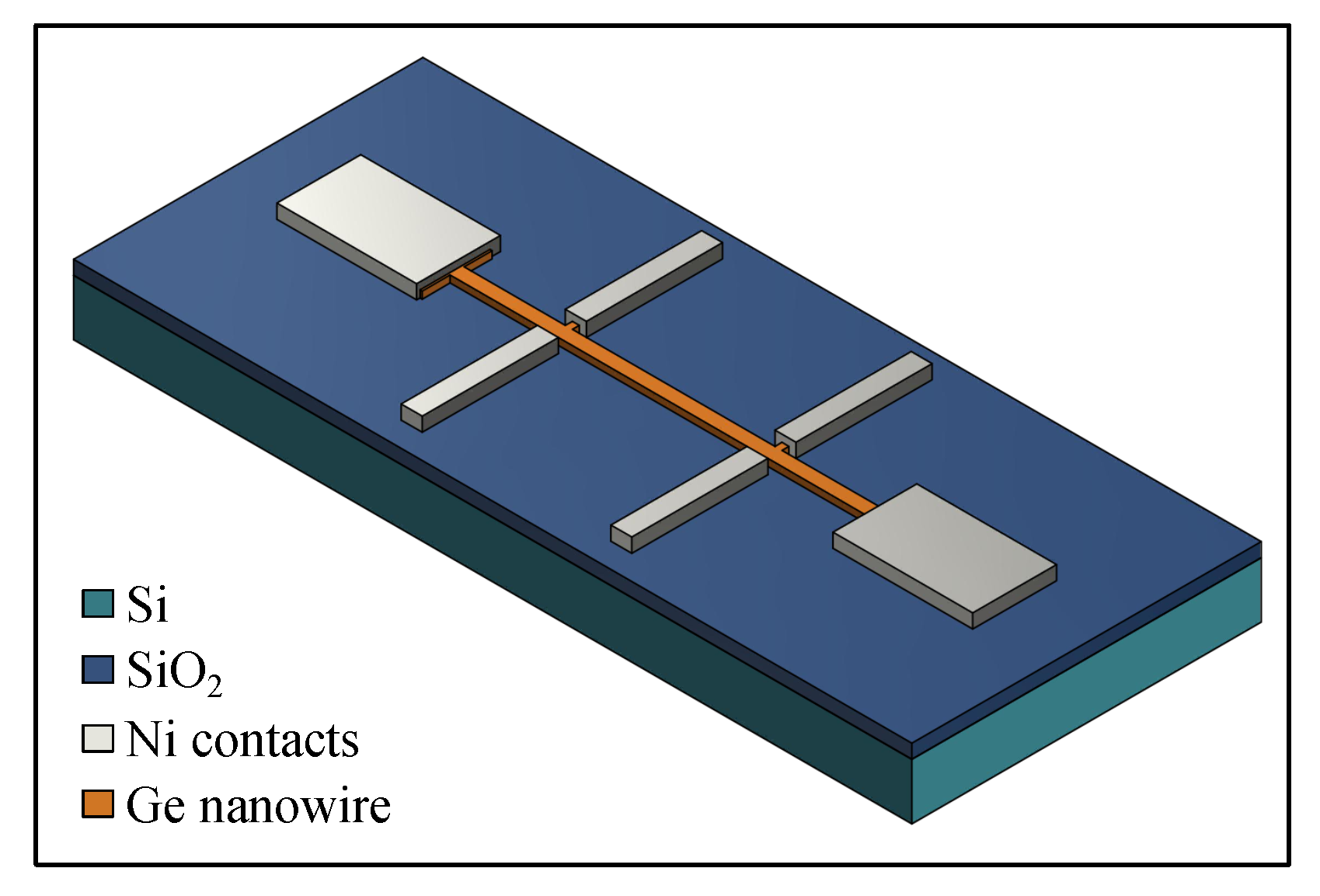
2.1. Experimental Setup
2.2. Modelling
3. Results and Discussion
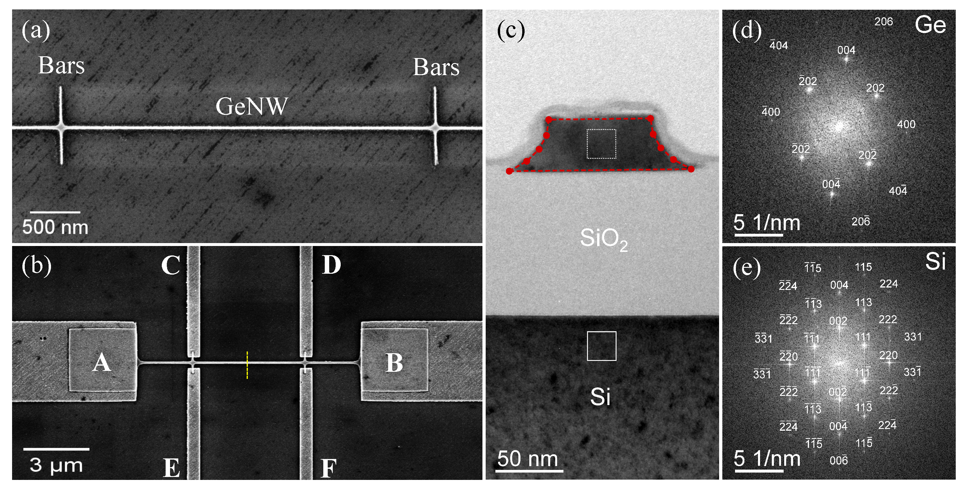
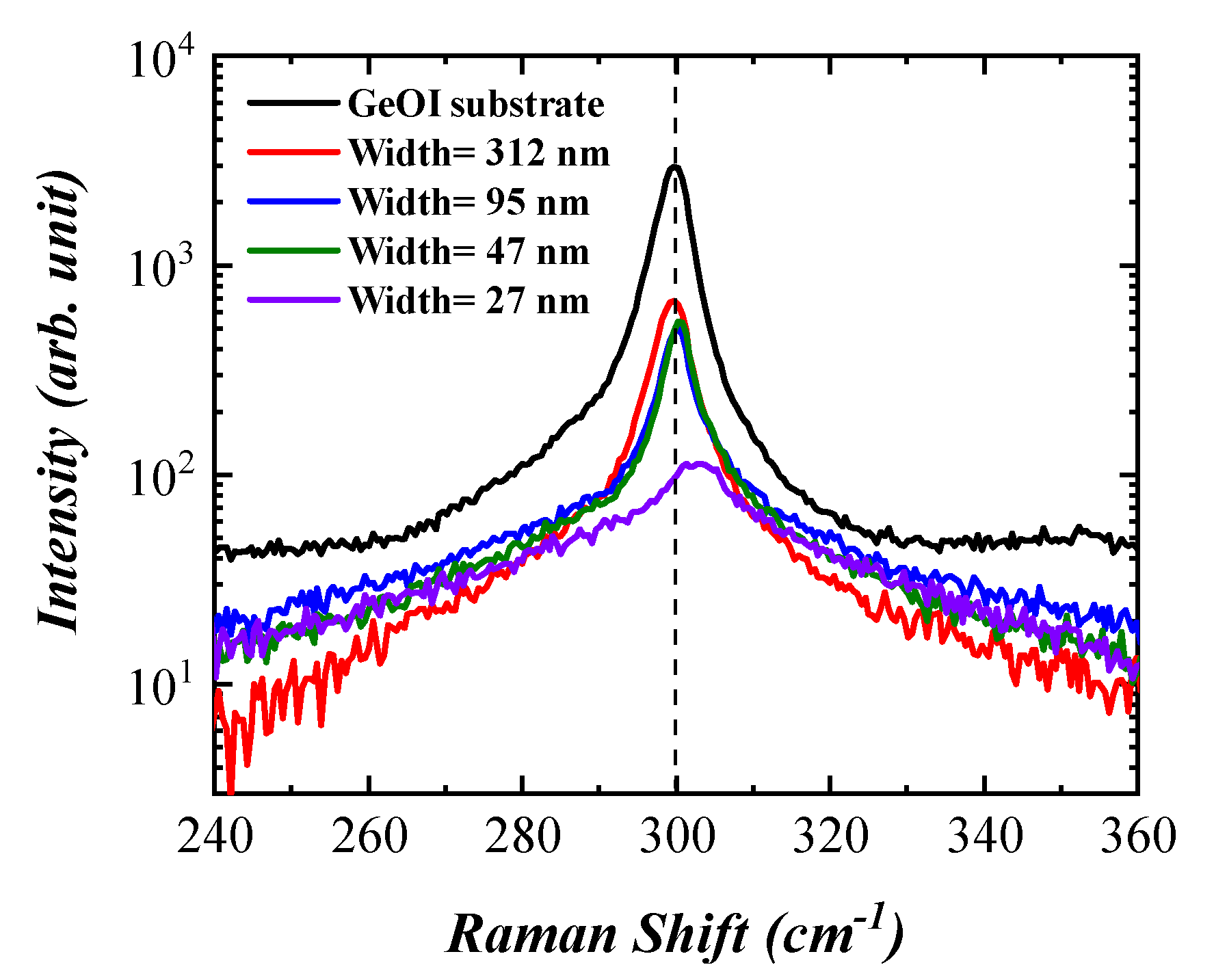
3.1. Structural Characterization
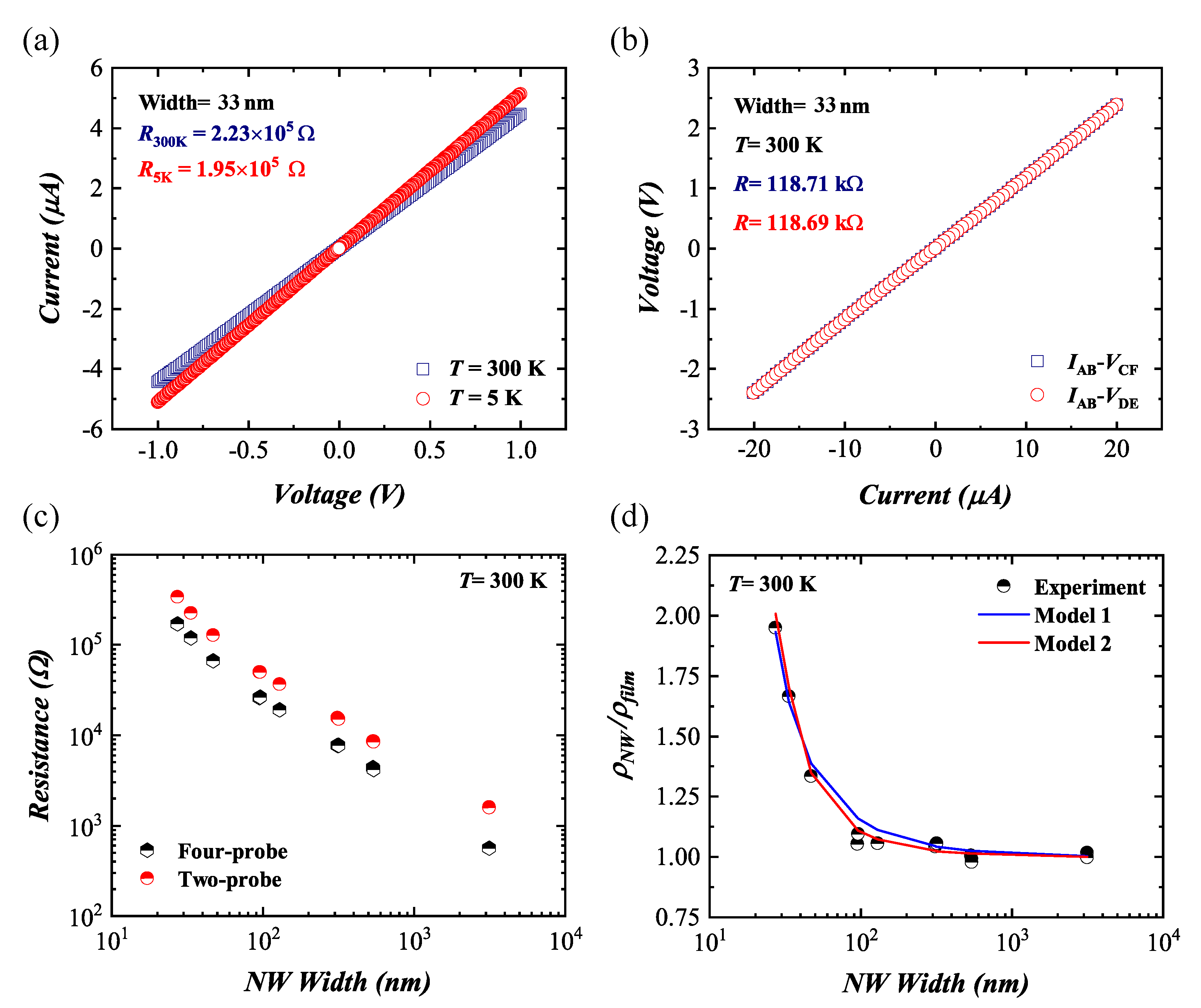
3.2. Two- and Four-Probe Measurements
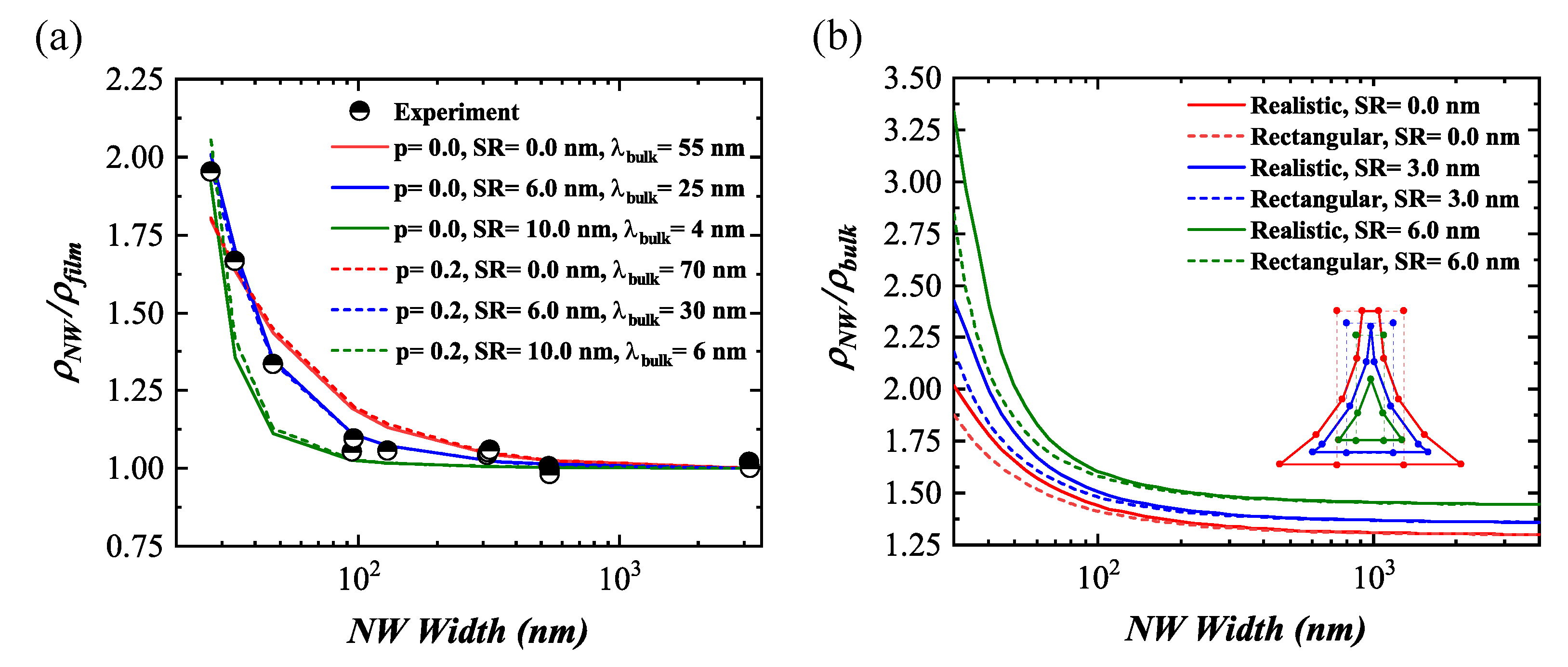
3.3. Simulated Normalized Resistivity
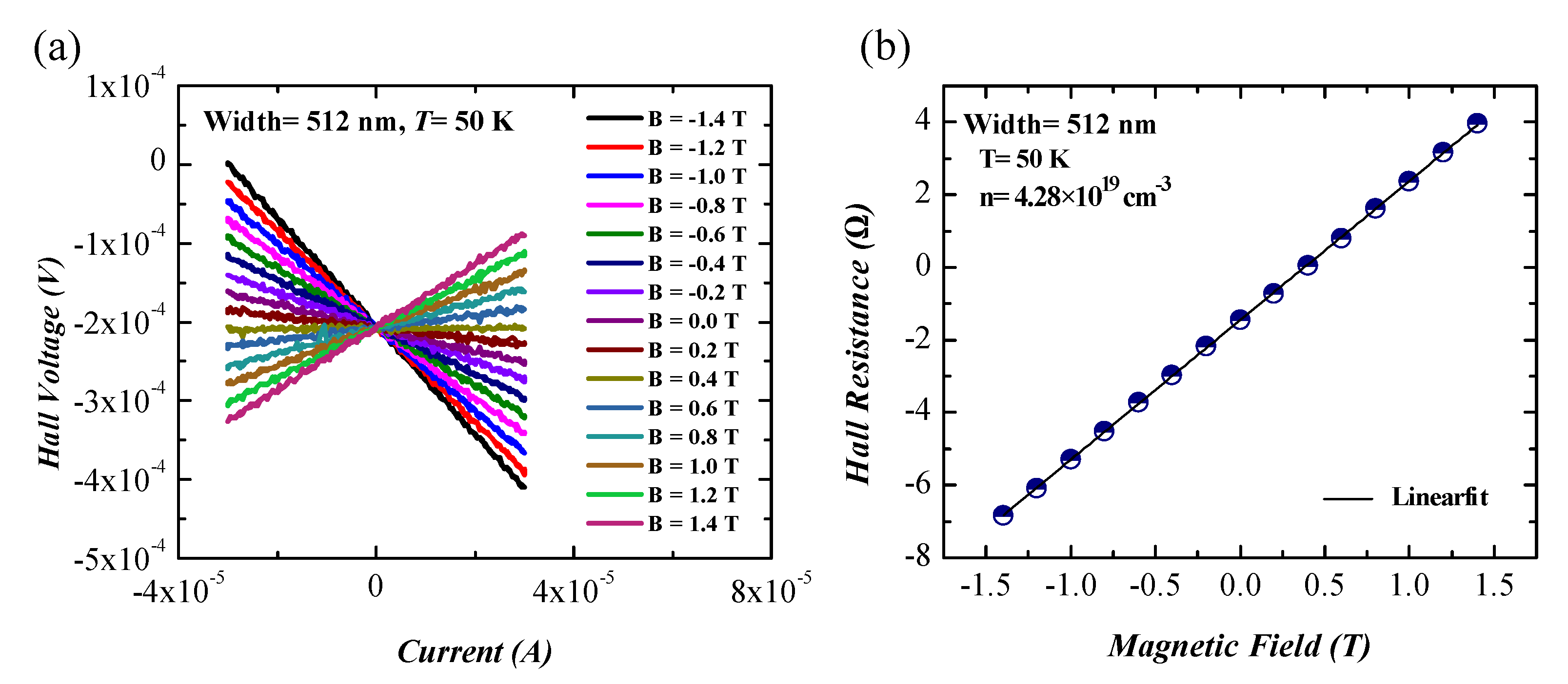
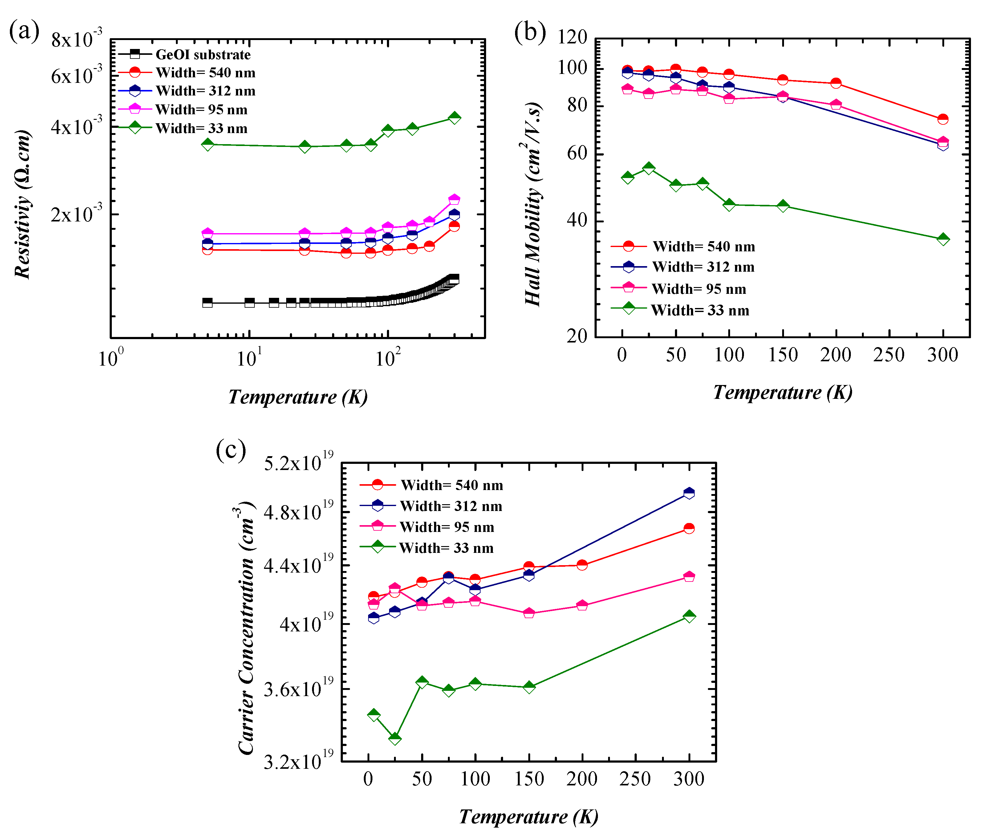
3.4. Hall Effect Measurement
3.5. Temperature-Dependent Measurement
4. Conclusions
Author Contributions
Funding
Institutional Review Board Statement
Informed Consent Statement
Data Availability Statement
Acknowledgments
Conflicts of Interest
References
- Duffy, R.; Shayesteh, M.; Thomas, K.; Pelucchi, E.; Yu, R.; Gangnaik, A.; Georgiev, Y.M.; Carolan, P.; Petkov, N.; Long, B.; et al. Access resistance reduction in Ge nanowires and substrates based on non-destructive gas-source dopant in-diffusion. J. Mater. Chem. C 2014, 2, 9248–9257. [Google Scholar] [CrossRef] [Green Version]
- Goley, P.S.; Hudait, M.K. Germanium based field-effect transistors: Challenges and opportunities. Materials 2014, 7, 2301–2339. [Google Scholar] [CrossRef] [PubMed]
- Sgourou, E.; Panayiotatos, Y.; Vovk, R.; Kuganathan, N.; Chroneos, A. Diffusion and Dopant Activation in Germanium: Insights from Recent Experimental and Theoretical Results. Appl. Sci. 2019, 9, 2454. [Google Scholar] [CrossRef] [Green Version]
- Tutuc, E.; Appenzeller, J.; Reuter, M.C.; Guha, S. Realization of a Linear Germanium Nanowire p- n Junction. Nano Lett. 2006, 6, 2070–2074. [Google Scholar] [CrossRef] [PubMed]
- Sistani, M.; Staudinger, P.; Lugstein, A. Polarity Control in Ge Nanowires by Electronic Surface Doping. J. Phys. Chem. C 2020, 124, 19858–19863. [Google Scholar] [CrossRef]
- John, J.W.; Dhyani, V.; Georgiev, Y.M.; Gangnaik, A.S.; Biswas, S.; Holmes, J.D.; Das, A.K.; Ray, S.K.; Das, S. Ultrahigh Negative Infrared Photoconductance in Highly As-Doped Germanium Nanowires Induced by Hot Electron Trapping. ACS Appl. Electron. Mater. 2020, 2, 1934–1942. [Google Scholar] [CrossRef]
- Zhang, S.; Hemesath, E.R.; Perea, D.E.; Wijaya, E.; Lensch-Falk, J.L.; Lauhon, L.J. Relative influence of surface states and bulk impurities on the electrical properties of Ge nanowires. Nano Lett. 2009, 9, 3268–3274. [Google Scholar] [CrossRef]
- Cui, Y.; Duan, X.; Hu, J.; Lieber, C.M. Doping and electrical transport in silicon nanowires. J. Phys. Chem. B 2000, 104, 5213–5216. [Google Scholar] [CrossRef]
- Garnett, E.C.; Tseng, Y.C.; Khanal, D.R.; Wu, J.; Bokor, J.; Yang, P. Dopant profiling and surface analysis of silicon nanowires using capacitance–voltage measurements. Nat. Nanotechnol. 2009, 4, 311–314. [Google Scholar] [CrossRef]
- Mansfield, L.; Bertness, K.A.; Blanchard, P.T.; Harvey, T.E.; Sanders, A.W.; Sanford, N.A. GaN nanowire carrier concentration calculated from light and dark resistance measurements. J. Electron. Mater. 2009, 38, 495–504. [Google Scholar] [CrossRef]
- Dufouleur, J.; Colombo, C.; Garma, T.; Ketterer, B.; Uccelli, E.; Nicotra, M.; Fontcuberta i Morral, A. P-doping mechanisms in catalyst-free gallium arsenide nanowires. Nano Lett. 2010, 10, 1734–1740. [Google Scholar] [CrossRef]
- Galluccio, E.; Doherty, J.; Biswas, S.; Holmes, J.D.; Duffy, R. Field-Effect Transistor Figures of Merit for Vapor–Liquid–Solid-Grown Ge1-xSn x (x = 0.03–0.09) Nanowire Devices. ACS Appl. Electron. Mater. 2020, 2, 1226–1234. [Google Scholar] [CrossRef]
- Wunnicke, O. Gate capacitance of back-gated nanowire field-effect transistors. Appl. Phys. Lett. 2006, 89, 083102. [Google Scholar] [CrossRef] [Green Version]
- Khanal, D.; Wu, J. Gate coupling and charge distribution in nanowire field effect transistors. Nano Lett. 2007, 7, 2778–2783. [Google Scholar] [CrossRef]
- Hultin, O.; Otnes, G.; Borgström, M.T.; Björk, M.; Samuelson, L.; Storm, K. Comparing Hall effect and field effect measurements on the same single nanowire. Nano Lett. 2016, 16, 205–211. [Google Scholar] [CrossRef] [PubMed]
- Hultin, O.; Otnes, G.; Samuelson, L.; Storm, K. Simplifying nanowire Hall effect characterization by using a three-probe device design. Nano Lett. 2017, 17, 1121–1126. [Google Scholar] [CrossRef]
- Storm, K.; Halvardsson, F.; Heurlin, M.; Lindgren, D.; Gustafsson, A.; Wu, P.M.; Monemar, B.; Samuelson, L. Spatially resolved Hall effect measurement in a single semiconductor nanowire. Nature Nanotechnol. 2012, 7, 718. [Google Scholar] [CrossRef] [PubMed] [Green Version]
- Blömers, C.; Grap, T.; Lepsa, M.; Moers, J.; Trellenkamp, S.; Grützmacher, D.; Lüth, H.; Schäpers, T. Hall effect measurements on InAs nanowires. Appl. Phys. Lett. 2012, 101, 152106. [Google Scholar] [CrossRef]
- Heurlin, M.; Hultin, O.; Storm, K.; Lindgren, D.; Borgström, M.T.; Samuelson, L. Synthesis of doped InP core–shell nanowires evaluated using hall effect measurements. Nano Lett. 2014, 14, 749–753. [Google Scholar] [CrossRef]
- Lindgren, D.; Hultin, O.; Heurlin, M.; Storm, K.; Borgström, M.T.; Samuelson, L.; Gustafsson, A. Study of carrier concentration in single InP nanowires by luminescence and Hall measurements. Nanotechnology 2015, 26, 045705. [Google Scholar] [CrossRef] [PubMed]
- DeGrave, J.P.; Liang, D.; Jin, S. A general method to measure the Hall effect in nanowires: Examples of FeS2 and MnSi. Nano Lett. 2013, 13, 2704–2709. [Google Scholar] [CrossRef]
- Verma, A.; Borisov, K.; Connaughton, S.; Stamenov, P. Hall Effect Measurements in Rotating Magnetic Field on Sub-30-nm Silicon Nanowires Fabricated by a Top–Down Approach. IEEE Trans. Electron Devices 2020, 67, 5201–5208. [Google Scholar] [CrossRef]
- Chen, K.; Zhao, X.; Mesli, A.; He, Y.; Dan, Y. Dynamics of charge carriers in silicon nanowire photoconductors revealed by photo Hall effect measurements. ACS Nano 2018, 12, 3436–3441. [Google Scholar] [CrossRef] [PubMed]
- Dong, R.; Han, P.; Arora, H.; Ballabio, M.; Karakus, M.; Zhang, Z.; Shekhar, C.; Adler, P.; Petkov, P.S.; Erbe, A.; et al. High-mobility band-like charge transport in a semiconducting two-dimensional metal–organic framework. Nat. Mater. 2018, 17, 1027–1032. [Google Scholar] [CrossRef]
- Look, D.C. Electrical Characterization of GaAs Materials and Devices; John Wiley & Sons: Chechister, UK, 1989. [Google Scholar]
- Namatsu, H.; Yamaguchi, T.; Nagase, M.; Yamazaki, K.; Kurihara, K. Nano-patterning of a hydrogen silsesquioxane resist with reduced linewidth fluctuations. Microelectron. Eng. 1998, 41, 331–334. [Google Scholar] [CrossRef]
- Georgiev, Y.; Henschel, W.; Fuchs, A.; Kurz, H. Surface roughness of hydrogen silsesquioxane as a negative tone electron beam resist. Vacuum 2005, 77, 117–123. [Google Scholar] [CrossRef]
- Mirza, M.M.; Zhou, H.; Velha, P.; Li, X.; Docherty, K.E.; Samarelli, A.; Ternent, G.; Paul, D.J. Nanofabrication of high aspect ratio (~50:1) sub-10 nm silicon nanowires using inductively coupled plasma etching. J. Vac. Sci. Technol. B Nanotechnol. Microelectron. Mater. Process. Meas. Phenom. 2012, 30, 06FF02. [Google Scholar] [CrossRef]
- Gangnaik, A.S.; Georgiev, Y.M.; Collins, G.; Holmes, J.D. Novel germanium surface modification for sub-10 nm patterning with electron beam lithography and hydrogen silsesquioxane resist. J. Vac. Sci. Technol. B Nanotechnol. Microelectron. Mater. Process. Meas. Phenom. 2016, 34, 041603. [Google Scholar] [CrossRef]
- Henschel, W.; Georgiev, Y.; Kurz, H. Study of a high contrast process for hydrogen silsesquioxane as a negative tone electron beam resist. J. Vac. Sci. Technol. B Microelectron. Nanometer Struct. Process. Meas. Phenom. 2003, 21, 2018–2025. [Google Scholar] [CrossRef]
- van der Pauw, L.J. A method of measuring the resistivity and Hall coefficient on lamellae of arbitrary shape. Philips Tech. Rev. 1958, 20, 220–224. [Google Scholar]
- Fuchs, K. The conductivity of thin metallic films according to the electron theory of metals. Math. Proc. Camb. Philos. Soc. 1938, 34, 100–108. [Google Scholar] [CrossRef]
- Dingle, R. The electrical conductivity of thin wires. Proc. R. Soc. Lond. Ser. A Math. Phys. Sci. 1950, 201, 545–560. [Google Scholar]
- Moraga, L.; Arenas, C.; Henriquez, R.; Solis, B. The effect of surface roughness and grain-boundary scattering on the electrical conductivity of thin metallic wires. Phys. Status Solidi 2015, 252, 219–229. [Google Scholar] [CrossRef]
- Chambers, R. The conductivity of thin wires in a magnetic field. Proc. R. Soc. Lond. Ser. A Math. Phys. Sci. 1950, 202, 378–394. [Google Scholar]
- Prucnal, S.; Berencén, Y.; Wang, M.; Grenzer, J.; Voelskow, M.; Hübner, R.; Yamamoto, Y.; Scheit, A.; Bärwolf, F.; Zviagin, V.; et al. Strain and band-gap engineering in Ge-Sn alloys via P doping. Phys. Rev. Appl. 2018, 10, 064055. [Google Scholar] [CrossRef] [Green Version]
- Osswald, S.; Mochalin, V.; Havel, M.; Yushin, G.; Gogotsi, Y. Phonon confinement effects in the Raman spectrum of nanodiamond. Phys. Rev. B 2009, 80, 075419. [Google Scholar] [CrossRef]
- Spizzirri, P.; Fang, J.H.; Rubanov, S.; Gauja, E.; Prawer, S. Nano-Raman spectroscopy of silicon surfaces. arXiv 2010, arXiv:1002.2692. [Google Scholar]
- Gallacher, K.; Velha, P.; Paul, D.J.; MacLaren, I.; Myronov, M.; Leadley, D.R. Ohmic contacts to n-type germanium with low specific contact resistivity. Appl. Phys. Lett. 2012, 100, 022113. [Google Scholar] [CrossRef] [Green Version]
- Lieten, R.; Degroote, S.; Kuijk, M.; Borghs, G. Ohmic contact formation on n-type Ge. Appl. Phys. Lett. 2008, 92, 022106. [Google Scholar] [CrossRef] [Green Version]
- Habanyama, A. Interface Control Processes for Ni/Ge and Pd/Ge Schottky and Ohmic Contact Fabrication: Part One. In Advanced Material and Device Applications with Germanium; IntechOpen: London, UK, 2018; p. 47. [Google Scholar] [CrossRef] [Green Version]
- Li, R.; Mi, L.; Wang, J.; Mao, M.; Gu, W.; Zhu, Y. Conductivity Size Effect of Square Cross-Section Polycrystalline Nanowires. Materials 2019, 12, 2129. [Google Scholar] [CrossRef] [Green Version]
- Xue, W.; Gu, W. Conductivity size effect of polycrystalline metal nanowires. AIP Adv. 2016, 6, 115001. [Google Scholar] [CrossRef] [Green Version]
- Seo, K.i.; Sharma, S.; Yasseri, A.A.; Stewart, D.R.; Kamins, T.I. Surface charge density of unpassivated and passivated metal-catalyzed silicon nanowires. Electrochem. Solid State Lett. 2006, 9, G69. [Google Scholar] [CrossRef]
- Simanullang, M.; Usami, K.; Noguchi, T.; Surawijaya, A.; Kodera, T.; Kawano, Y.; Oda, S. Surface passivation of germanium nanowires using Al2O3 and HfO2 deposited via atomic layer deposition technique. Jpn. J. Appl. Phys. 2014, 53, 06JG04. [Google Scholar] [CrossRef]
- Colinge, J.P.; Colinge, C.A. Physics of Semiconductor Devices; Kluwer Academic Publishers: New York, NY, USA, 2005. [Google Scholar]
- Ou, X.; Kanungo, P.D.; Kögler, R.; Werner, P.; Gösele, U.; Skorupa, W.; Wang, X. Three-Dimensional Carrier Profiling of Individual Si Nanowires by Scanning Spreading Resistance Microscopy. Adv. Mater. 2010, 22, 4020–4024. [Google Scholar] [CrossRef]
- Björk, M.T.; Schmid, H.; Knoch, J.; Riel, H.; Riess, W. Donor deactivation in silicon nanostructures. Nat. Nanotechnol. 2009, 4, 103–107. [Google Scholar] [CrossRef]
- Diarra, M.; Niquet, Y.M.; Delerue, C.; Allan, G. Ionization energy of donor and acceptor impurities in semiconductor nanowires: Importance of dielectric confinement. Phys. Rev. B 2007, 75, 045301. [Google Scholar] [CrossRef] [Green Version]
- Nguyen, B.M.; Taur, Y.; Picraux, S.T.; Dayeh, S.A. Diameter-independent hole mobility in Ge/Si core/shell nanowire field effect transistors. Nano Lett. 2014, 14, 585–591. [Google Scholar] [CrossRef] [PubMed]
- Niquet, Y.M.; Delerue, C. Carrier mobility in strained Ge nanowires. J. Appl. Phys. 2012, 112, 084301. [Google Scholar] [CrossRef]
- Moto, K.; Yoshimine, R.; Suemasu, T.; Toko, K. Improving carrier mobility of polycrystalline Ge by Sn doping. Sci. Rep. 2018, 8, 1–7. [Google Scholar]


| NW Width (nm) | cm) | cm | ||
|---|---|---|---|---|
| 3156 | 1.87 | 4.28 | 78.0 | 9.3 |
| 540 | 1.81 | 4.67 | 73.8 | 8.8 |
| 312 | 1.99 | 4.94 | 63.3 | 7.5 |
| 95 | 2.24 | 4.32 | 64.4 | 7.7 |
| 33 | 4.29 | 4.05 | 35.9 | 4.3 |
Publisher’s Note: MDPI stays neutral with regard to jurisdictional claims in published maps and institutional affiliations. |
© 2021 by the authors. Licensee MDPI, Basel, Switzerland. This article is an open access article distributed under the terms and conditions of the Creative Commons Attribution (CC BY) license (https://creativecommons.org/licenses/by/4.0/).
Share and Cite
Echresh, A.; Arora, H.; Fuchs, F.; Li, Z.; Hübner, R.; Prucnal, S.; Schuster, J.; Zahn, P.; Helm, M.; Zhou, S.; et al. Electrical Characterization of Germanium Nanowires Using a Symmetric Hall Bar Configuration: Size and Shape Dependence. Nanomaterials 2021, 11, 2917. https://doi.org/10.3390/nano11112917
Echresh A, Arora H, Fuchs F, Li Z, Hübner R, Prucnal S, Schuster J, Zahn P, Helm M, Zhou S, et al. Electrical Characterization of Germanium Nanowires Using a Symmetric Hall Bar Configuration: Size and Shape Dependence. Nanomaterials. 2021; 11(11):2917. https://doi.org/10.3390/nano11112917
Chicago/Turabian StyleEchresh, Ahmad, Himani Arora, Florian Fuchs, Zichao Li, René Hübner, Slawomir Prucnal, Jörg Schuster, Peter Zahn, Manfred Helm, Shengqiang Zhou, and et al. 2021. "Electrical Characterization of Germanium Nanowires Using a Symmetric Hall Bar Configuration: Size and Shape Dependence" Nanomaterials 11, no. 11: 2917. https://doi.org/10.3390/nano11112917
APA StyleEchresh, A., Arora, H., Fuchs, F., Li, Z., Hübner, R., Prucnal, S., Schuster, J., Zahn, P., Helm, M., Zhou, S., Erbe, A., Rebohle, L., & Georgiev, Y. M. (2021). Electrical Characterization of Germanium Nanowires Using a Symmetric Hall Bar Configuration: Size and Shape Dependence. Nanomaterials, 11(11), 2917. https://doi.org/10.3390/nano11112917