
Hierarchically Porous, Laser-Pyrolyzed Carbon Electrode from Black Photoresist for On-Chip Microsupercapacitors

 , , ,
, , , 
Abstract
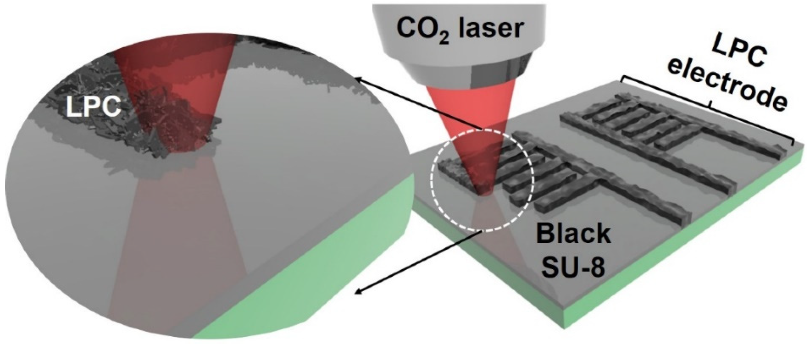
:1. Introduction
2. Experimental Setup
2.1. Materials
2.2. Material Preparation
2.3. Characterization
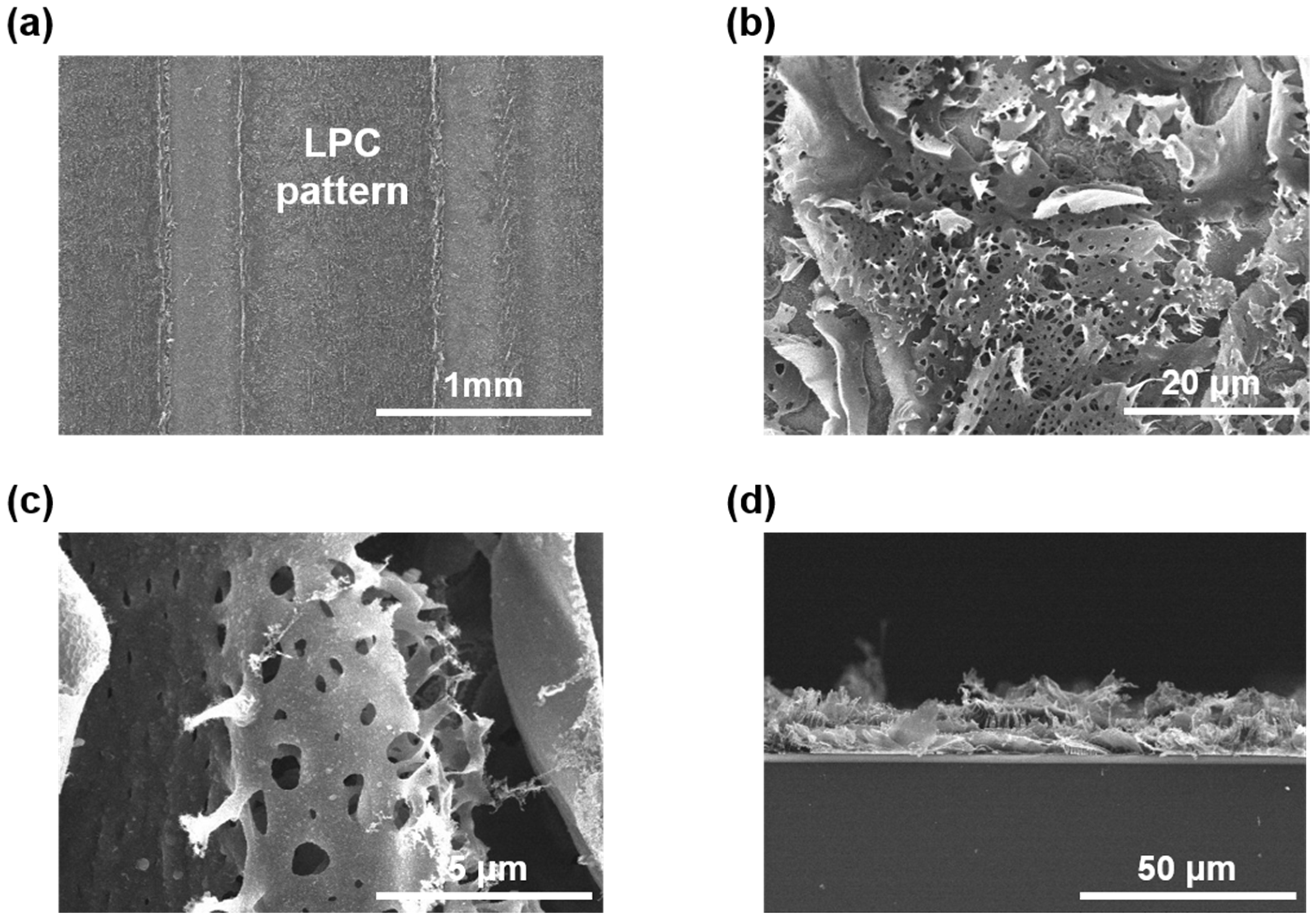
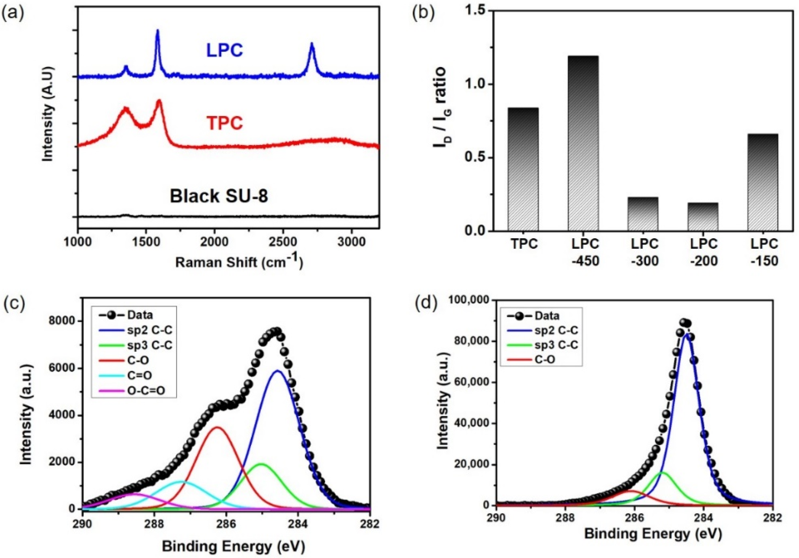
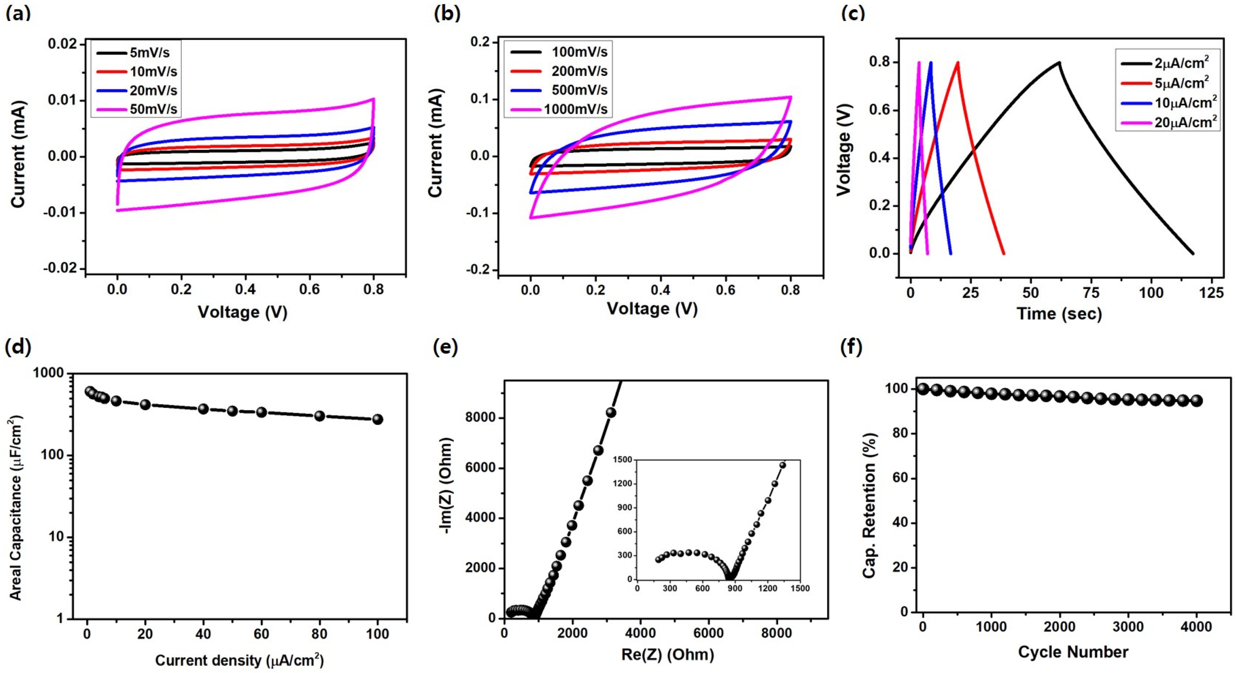
3. Results and Discussions
4. Conclusions
Supplementary Materials
Author Contributions
Funding
Data Availability Statement
Acknowledgments
Conflicts of Interest
References
- Huang, P.; Lethien, C.; Pinaud, S.; Brousse, K.; Laloo, R.; Turq, V.; Respaud, M.; Demortiere, A.; Daffos, B.; Taberna, P.L.; et al. On-chip and freestanding elastic carbon films for micro-supercapacitors. Science 2016, 351, 691–695. [Google Scholar] [CrossRef] [Green Version]
- Kyreremateng, N.A.; Brousse, T.; Pech, D. Microsupercapacitors as miniaturized energy-storage components for on-chip electronics. Nat. Nanotechnol. 2017, 12, 7–15. [Google Scholar] [CrossRef]
- Jia, R.; Shen, G.; Qu, F.; Chen, D. Flexible on-chip micro-supercapacitors: Efficient power units for wearable electronics. Energy Stroage Mater. 2020, 27, 169–186. [Google Scholar] [CrossRef]
- Qi, D.; Liu, Y.; Liu, Z.; Zhang, L.; Chen, X. Design of Architectures and Materials in In-Plane Micro-supercapacitors: Current Status and Future Challenges. Adv. Mater. 2017, 29, 1602802. [Google Scholar] [CrossRef]
- Guo, R.; Chen, J.; Yang, B.; Liu, L.; Su, L.; Shen, B.; Yan, X. In-Plane Micro-Supercapacitors for an Integrated Device on One Piece of Paper. Adv. Funct. Mater. 2017, 27, 1702394. [Google Scholar] [CrossRef]
- Kim, S.-W.; Kang, K.-N.; Min, J.-W.; Jang, J.-H. Plotter-assisted integration of wearable all-solid-state micro-supercapacitors. Nano Energy 2018, 50, 410–416. [Google Scholar] [CrossRef]
- Choi, K.-H.; Yoo, J.; Lee, C.K.; Lee, S.-Y. All-inkjet-printed, solid-state flexible supercapacitors on paper. Energy Environ. Sci. 2016, 9, 2812–2821. [Google Scholar] [CrossRef]
- Secor, E.B.; Lim, S.; Zhang, H.; Frisbie, C.D.; Francis, L.F.; Hersam, M.C. Gravure printing of graphene for large-area flexible electronics. Adv. Mater. 2014, 26, 4533–4538. [Google Scholar] [CrossRef]
- Zhang, C.; McKeon, L.; Kremer, M.P.; Park, S.-H.; Ronan, O.; Seral-Ascaso, A.; Barwich, S.; Coileáin, C.; McEvoy, N.; Nerl, H.C.; et al. Additive-free MXene inks and direct printing of micro-supercapacitors. Nat. Commun. 2019, 10, 1795. [Google Scholar] [CrossRef] [PubMed]
- Beidaghi, M.; Wang, C. Micro-supercapacitors based on three-dimensional interdigital polypyrrole/c-mems electrodes. Electrochim. Acta 2011, 56, 9508–9514. [Google Scholar] [CrossRef]
- Hsia, B.; Kim, M.S.; Vincent, M.; Carraro, C.; Maboudian, R. Photoresist-derived porous carbon for on-chip micro-supercapacitors. Carbon 2013, 57, 395–400. [Google Scholar] [CrossRef]
- Wang, S.; Hsia, B.; Carraro, C.; Maboudian, R. High-performance all solid-state micro-supercapacitor based on patterned photoresist-derived porous carbon electrodes and an ionogel electrolyte. J. Mater. Chem. A 2014, 2, 7997. [Google Scholar] [CrossRef]
- Kim, M.S.; Hsia, B.; Carraro, C.; Maboudian, R. Flexible micro-supercapacitors with high energy density from simple transfer of photoresist-derived porous carbon electrodes. Carbon 2014, 74, 163–169. [Google Scholar] [CrossRef]
- Hemanth, S.; Caviglia, C.; Keller, S.S. Suspended 3D pyrolytic carbon microelectrodes for electrochemistry. Carbon 2017, 121, 226–234. [Google Scholar] [CrossRef] [Green Version]
- Natu, R.; Islam, M.; Gilmore, J.; Martinez-Duarte, R. Shrinkage of SU-8 microstructures during carbonization. J. Anal. Appl. Pyrolysis 2018, 131, 17–27. [Google Scholar] [CrossRef]
- Go, D.; Lott, P.; Stollenwerk, J.; Thomas, H.; Moller, M.; Kuehne, A.J.C. Laser carbonization of PAN-nanofiber mats with enhanced surface area and porosity. ACS Appl. Mater. Interfaces 2016, 8, 28412–28417. [Google Scholar] [CrossRef] [PubMed]
- Rao, Y.; Yuan, M.; Luo, F.; Wang, Z.; Li, H.; Yu, J.; Chen, X. One-step laser fabrication of phosphorus-doped porous graphene electrodes for high-performance flexible microsupercapacitors. Carbon 2021, 180, 56–66. [Google Scholar] [CrossRef]
- Beckham, J.L.; Li, J.T.; Stanford, M.G.; Chen, W.; McHugh, E.A.; Advincular, P.A.; Wyss, K.M.; Chyan, Y.; Boldman, W.L.; Rack, P.D.; et al. High-resolution laser-induced graphene from photoresist. ACS Nano 2021, 15, 8976–8983. [Google Scholar] [CrossRef] [PubMed]
- Yuan, M.; Luo, F.; Rao, Y.; Yu, J.; Wang, Z.; Li, H.; Chen, X. SWCNT-bridged laser-induced graphene fibers decorated with MnO2 nanoparticles for high-performance flexible micro-supercapacitors. Carbon 2021, 183, 128–137. [Google Scholar] [CrossRef]
- Cai, J.; Lv, C.; Watanabe, A. Laser direct writing of high-performance flexible all-solid-state carbon micro-supercapacitors for an on-chip self-powered photodetection system. Nano Energy 2016, 30, 790–800. [Google Scholar] [CrossRef]
- Zang, X.; Shen, C.; Chu, Y.; Li, B.; Wei, M.; Zhong, J.; Sanghadasa, M.; Lin, L. Laser-Induced Molybdenum Carbide–Graphene Composites for 3D Foldable Paper Electronics. Adv. Mater. 2018, 30, 1800062. [Google Scholar] [CrossRef]
- Basu, A.; Roy, K.; Sharma, N.; Nandi, S.; Vaidhyanathan, R.; Rane, S.; Rode, C.; Ogale, S. CO2 laser direct written MOF-based metal-decorated and heteroatom-doped porous graphene for flexible all-solid-state microsupercapacitor with extremely high cycling stability. ACS Appl. Mater. Interfaces 2016, 8, 31841–31848. [Google Scholar] [CrossRef]
- Kwon, S.; Lee, T.; Choi, H.-J.; Ahn, J.; Lim, H.; Kim, G.; Choi, K.-B.; Lee, J. Scalable fabrication of inkless, transfer-printed graphene-based textile microsupercapacitors with high rate capabilities. J. Power Sources 2021, 481, 228939. [Google Scholar] [CrossRef]
- Do, M.T.; Li, Q.; Nguten, T.T.N.; Benisty, H.; Ledoux-Rak, I.; Lai, N.D. High aspect ratio submicrometer two-dimensional structures fabricated by one-photon absorption direct laser writing. Microsyst. Technol. 2014, 20, 2097–2102. [Google Scholar] [CrossRef]
- Ludvigsen, E.; Pedersen, N.R.; Zhu, X.; Marie, R.; Mackenzie, D.M.A.; Emneus, J.; Petersen, D.H.; Kristensen, A.; Keller, S.S. Selective direct laser writing of pyrolytic carbon microelectrodes in absorber-modified SU-8. Micromachines 2021, 12, 564. [Google Scholar] [CrossRef] [PubMed]
- Schniepp, H.C.; Li, J.; McAllister, M.J.; Sai, H.; Herrera-Alonso, M.; Adamson, D.H.; Prud’homme, R.K.; Car, R.; Saville, D.A.; Aksay, I.A. Functionalized single graphene sheets derived from splitting graphite oxide. J. Phys. Chem. B 2006, 110, 8535–8539. [Google Scholar] [CrossRef] [PubMed] [Green Version]
- McAllister, M.J.; Li, J.; Adamson, D.H.; Schniepp, H.C.; Abdala, A.A.; Liu, J.; Herrera-Alonso, M.; Milius, D.L.; Car, R.; Prud’homme, R.K.; et al. Single sheet functionalized graphene by oxidation and thermal expansion of graphite. Chem. Mater. 2007, 19, 4396–4404. [Google Scholar] [CrossRef]
- Kwon, S.; Yoon, Y.; Ahn, J.; Lim, H.; Kim, G.; Kim, J.-H.; Choi, K.-B.; Lee, J. Facile laser fabrication of high quality graphene-based microsupercapacitors with large capacitance. Carbon 2018, 137, 136–145. [Google Scholar] [CrossRef]
- Chyan, Y.; Ye, R.; Li, Y.; Singh, S.P.; Arnusch, C.J.; Tour, J.M. Laser-Induced Graphene by Multiple Lasing: Toward Electronics on Cloth, Paper, and Food. ACS Nano 2018, 12, 2176–2183. [Google Scholar] [CrossRef]
- Cançado, L.G.; Takai, K.; Enoki, T.; Endo, M.; Kim, Y.A.; Mizusaki, H.; Jorio, A.; Coelho, L.N.; Magalhaes-Paniago, R.; Pimenta, M.A. General equation for the determination of the crystallite size L a of nanographite by Raman spectroscopy. Appl. Phys. Lett. 2006, 88, 163106. [Google Scholar] [CrossRef]
- Mardegan, A.; Kamath, R.; Sharma, S.; Scopece, P.; Ugo, P.; Madou, M. Optimization of carbon electrodes derived from epoxy-based photoresist. J. Electrochem. Soc. 2013, 160, B132–B137. [Google Scholar] [CrossRef] [Green Version]
- Kang, D.-Y.; Kim, C.; Park, G.; Moon, J.H. Liquid immersion thermal crosslinking of 3D polymer nanopatterns for direct carbonization with high structural integrity. Sci. Rep. 2015, 5, 18185. [Google Scholar] [CrossRef] [Green Version]
- Yang, D.; Velamakanni, A.; Bozoklu, G.; Park, S.; Stoller, M.; Piner, R.D.; Stankovich, S.; Jung, I.; Field, D.A.; Ventrice, C.A., Jr.; et al. Chemical analysis of graphene oxide films after heat and chemical treatments by X-ray photoelectron and Micro-Raman spectroscopy. Carbon 2009, 47, 145–152. [Google Scholar] [CrossRef]
- Shin, H.-J.; Kim, K.K.; Benayad, A.; Yoon, S.-M.; Park, H.K.; Jung, I.-S.; Jin, M.H.; Jeong, H.-K.; Kim, J.M.; Choi, J.-H.; et al. Efficient reduction of graphite oxide by sodium borohydride and its effect on electrical conductance. Adv. Funct. Mater. 2009, 19, 1987–1992. [Google Scholar] [CrossRef]
- Some, S.; Kim, Y.; Yoon, Y.; Yoo, H.; Lee, S.; Park, Y.; Lee, H. High-quality reduced graphene oxide by a dual-function chemical reduction and healing process. Sci. Rep. 2013, 3, 1929. [Google Scholar] [CrossRef] [Green Version]
- Yung, K.C.; Liem, H.; Choy, H.S.; Chen, Z.C.; Cheng, K.H.; Cai, Z.X. Laser direct patterning of a reduced-graphene oxide transparent circuit on a graphene oxide thin film. J. Appl. Phys. 2013, 113, 244903. [Google Scholar] [CrossRef]
- Lin, J.; Peng, Z.; Liu, Y.; Ruiz-Zepeda, F.; Ye, R.; Samuel, E.L.G.; Yacaman, M.J.; Yakobson, B.I.; Tour, J.M. Laser-induced porous graphene films from commercial polymers. Nat. Commun. 2014, 5, 5714. [Google Scholar] [CrossRef] [PubMed]
- Pei, S.; Cheng, H.M. The reduction of graphene oxide. Carbon 2012, 50, 3210–3228. [Google Scholar] [CrossRef]
- Du, R.; Sseyange, S.; Aktary, M.; McDermott, M.T. Fabrication and characterization of graphitic carbon nanostructures with controllable size, shape, and position. Small 2009, 5, 1162–1168. [Google Scholar] [CrossRef]
- Kim, D.; Pramanick, B.; Salazar, A.; Tcho, I.-W.; Madou, M.J.; Jung, E.S.; Choi, Y.-K.; Hwang, H. 3D carbon electrode based triboelectric nanogenerator. Adv. Mater. Technol. 2016, 1, 1600160. [Google Scholar] [CrossRef]
- Kwon, S.; Kim, G.; Lim, H.; Kim, J.; Choi, K.-B.; Lee, J. High performance microsupercapacitors based on nano-micro hierarchical carbon electrode by direct laser writing. Appl. Phys. Lett. 2018, 113, 243901. [Google Scholar] [CrossRef]
- Jang, J.; Yeom, J.W.; Kang, W.K.; Haq, M.R.; Lu, X.; Shin, D.; Kim, S.-M.; In, J.B. Laser pyrolysis of imprinted furan pattern for the precise fabrication of microsupercapacitor electrodes. Micromachines 2020, 11, 746. [Google Scholar] [CrossRef] [PubMed]

Publisher’s Note: MDPI stays neutral with regard to jurisdictional claims in published maps and institutional affiliations. |
© 2021 by the authors. Licensee MDPI, Basel, Switzerland. This article is an open access article distributed under the terms and conditions of the Creative Commons Attribution (CC BY) license (https://creativecommons.org/licenses/by/4.0/).
Share and Cite
Kwon, S.; Choi, H.-J.; Shim, H.C.; Yoon, Y.; Ahn, J.; Lim, H.; Kim, G.; Choi, K.-B.; Lee, J. Hierarchically Porous, Laser-Pyrolyzed Carbon Electrode from Black Photoresist for On-Chip Microsupercapacitors. Nanomaterials 2021, 11, 2828. https://doi.org/10.3390/nano11112828
Kwon S, Choi H-J, Shim HC, Yoon Y, Ahn J, Lim H, Kim G, Choi K-B, Lee J. Hierarchically Porous, Laser-Pyrolyzed Carbon Electrode from Black Photoresist for On-Chip Microsupercapacitors. Nanomaterials. 2021; 11(11):2828. https://doi.org/10.3390/nano11112828
Chicago/Turabian StyleKwon, Soongeun, Hak-Jong Choi, Hyung Cheoul Shim, Yeoheung Yoon, Junhyoung Ahn, Hyungjun Lim, Geehong Kim, Kee-Bong Choi, and JaeJong Lee. 2021. "Hierarchically Porous, Laser-Pyrolyzed Carbon Electrode from Black Photoresist for On-Chip Microsupercapacitors" Nanomaterials 11, no. 11: 2828. https://doi.org/10.3390/nano11112828
APA StyleKwon, S., Choi, H.-J., Shim, H. C., Yoon, Y., Ahn, J., Lim, H., Kim, G., Choi, K.-B., & Lee, J. (2021). Hierarchically Porous, Laser-Pyrolyzed Carbon Electrode from Black Photoresist for On-Chip Microsupercapacitors. Nanomaterials, 11(11), 2828. https://doi.org/10.3390/nano11112828