Color Centers Enabled by Direct Femto-Second Laser Writing in Wide Bandgap Semiconductors

 ,
,  ,
, 
Abstract
1. Introduction
2. Light–Matter Interaction
3. Materials and Methods
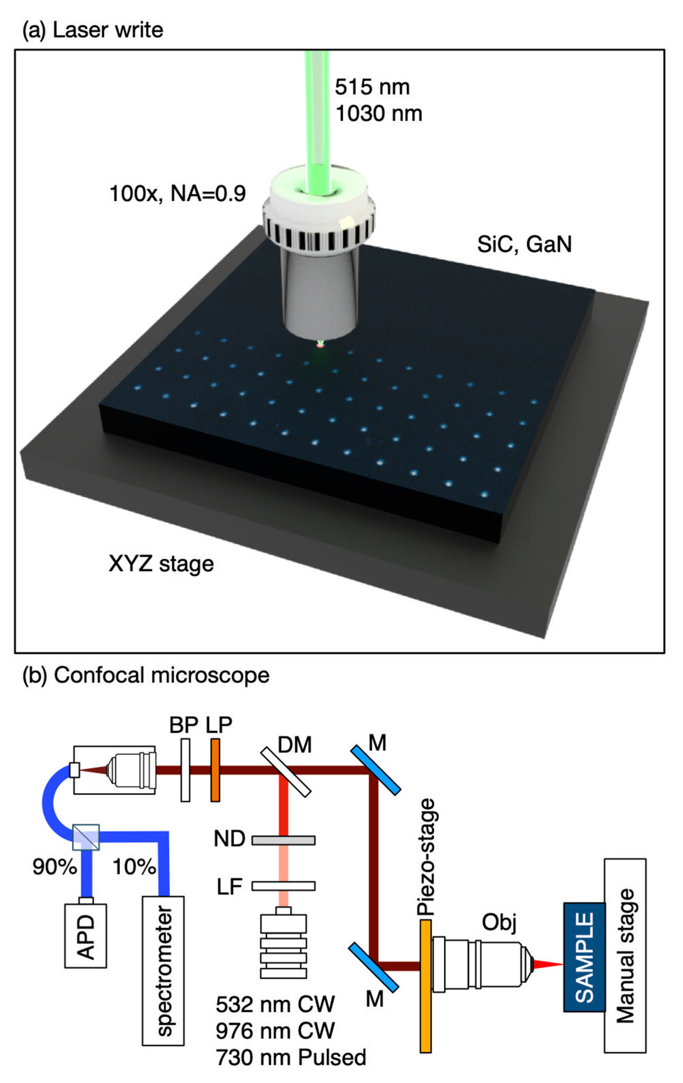
3.1. Laser Inscription
3.2. Photoluminescence Mapping
4. Results and Discussion
4.1. Laser Writing at 515 nm
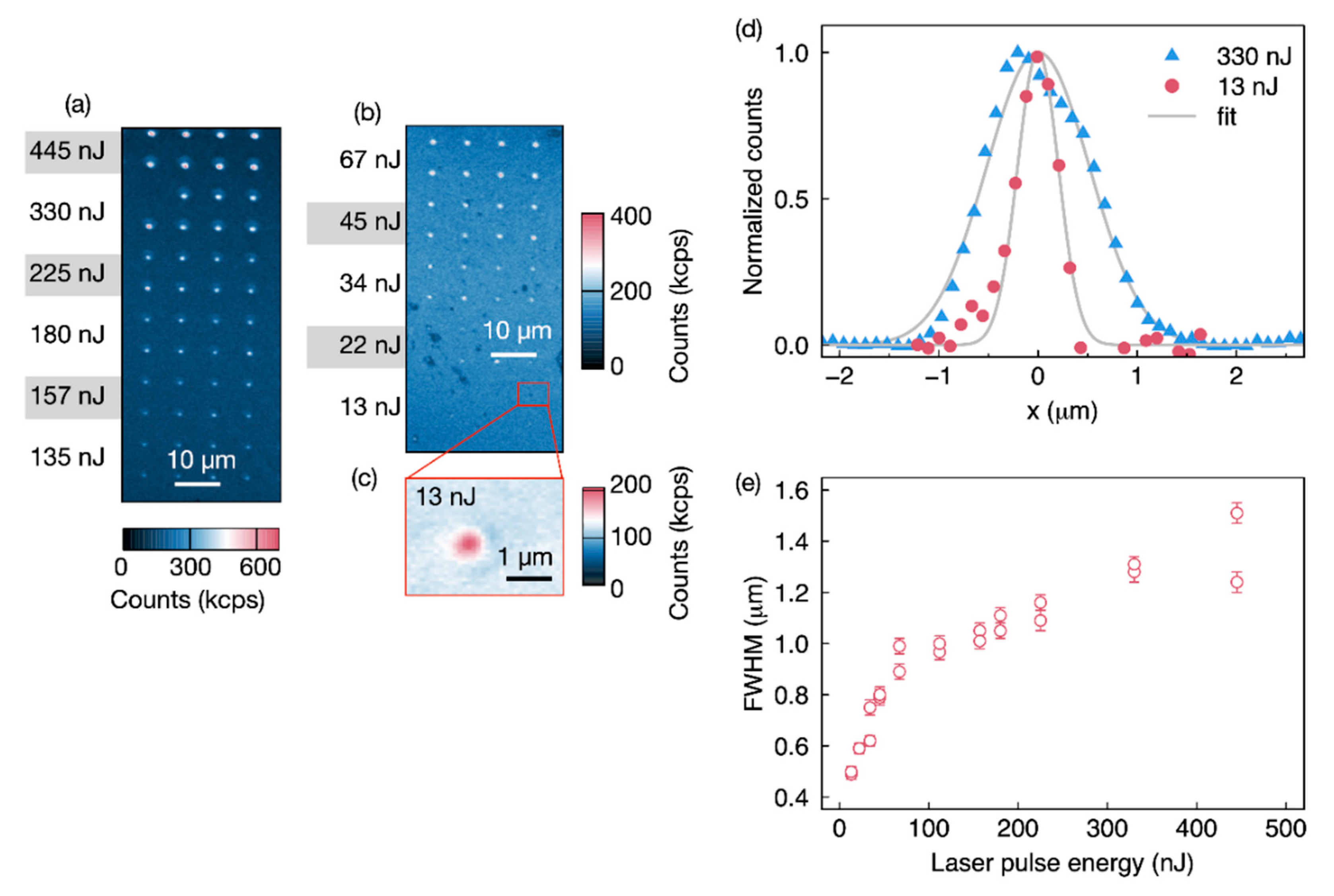
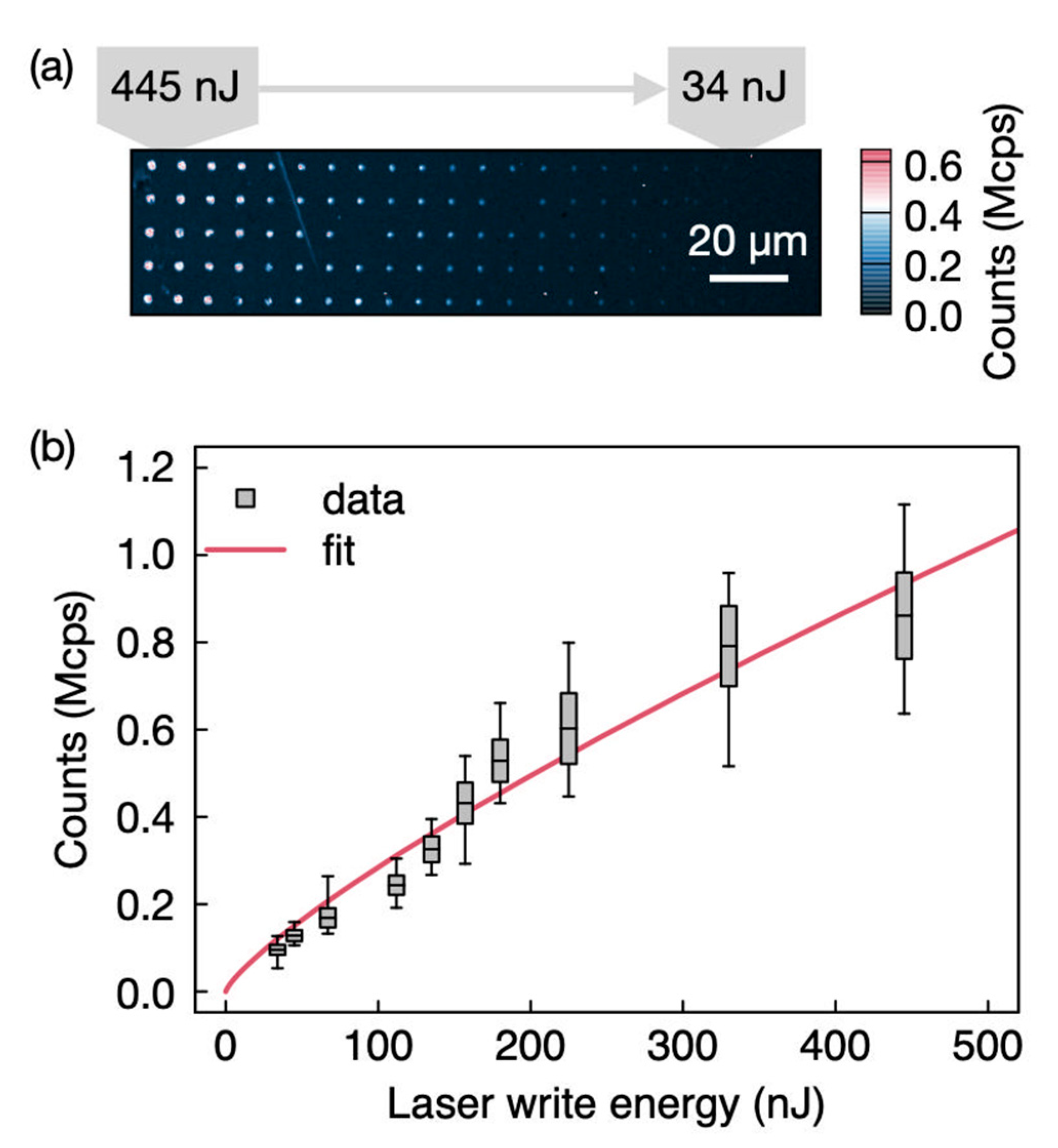
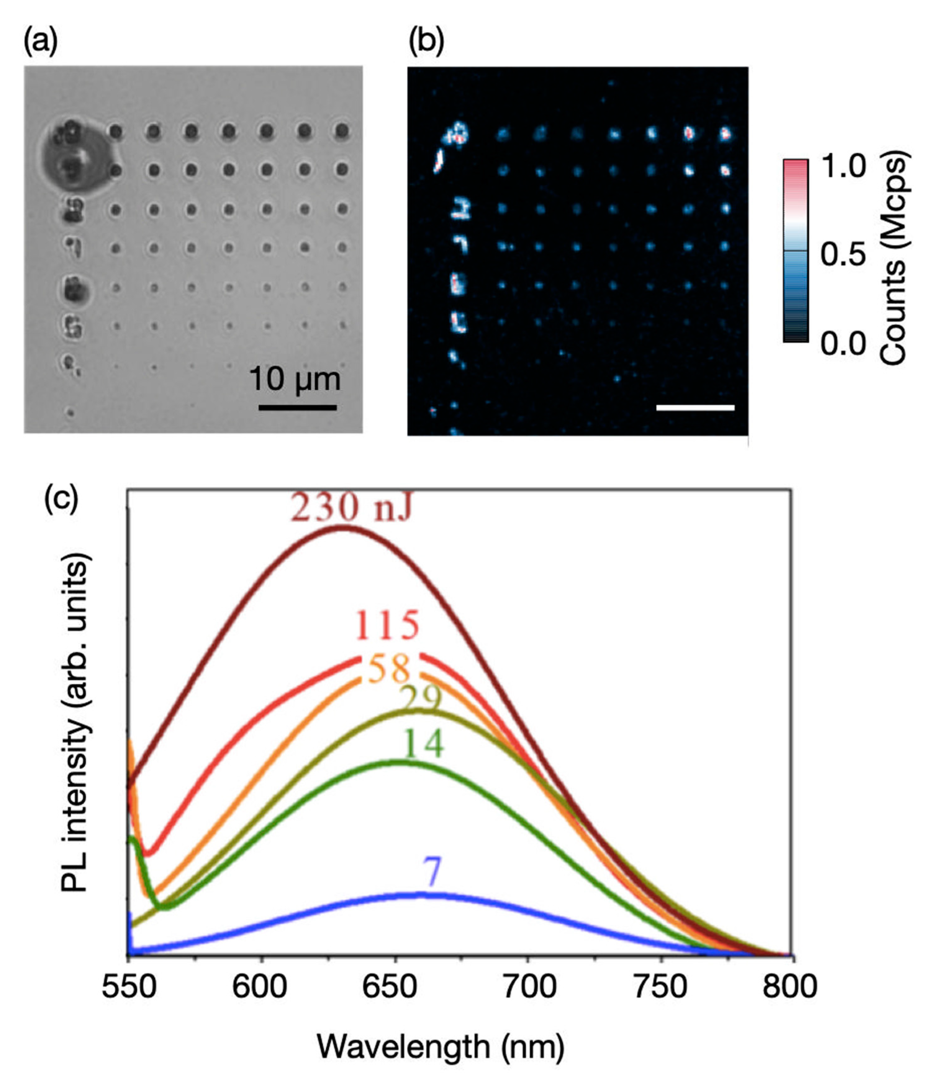
4.1.1. High Purity Semi-Insulating 4H-SiC: Confocal Maps
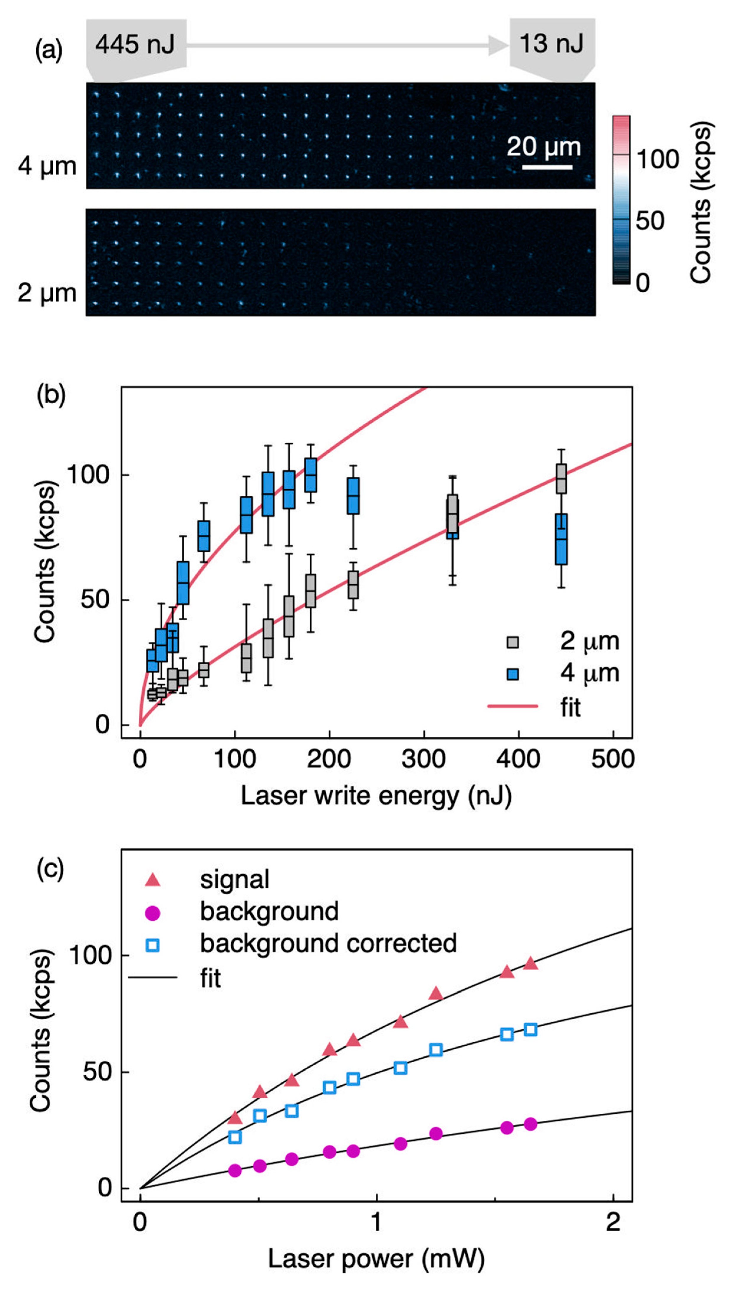
4.1.2. n-Type 4H-SiC: Confocal Maps
4.1.3. PL from High-Purity Semi-Insulating 4H-SiC
4.2. Laser Writing at 1030 nm
4.2.1. GaN
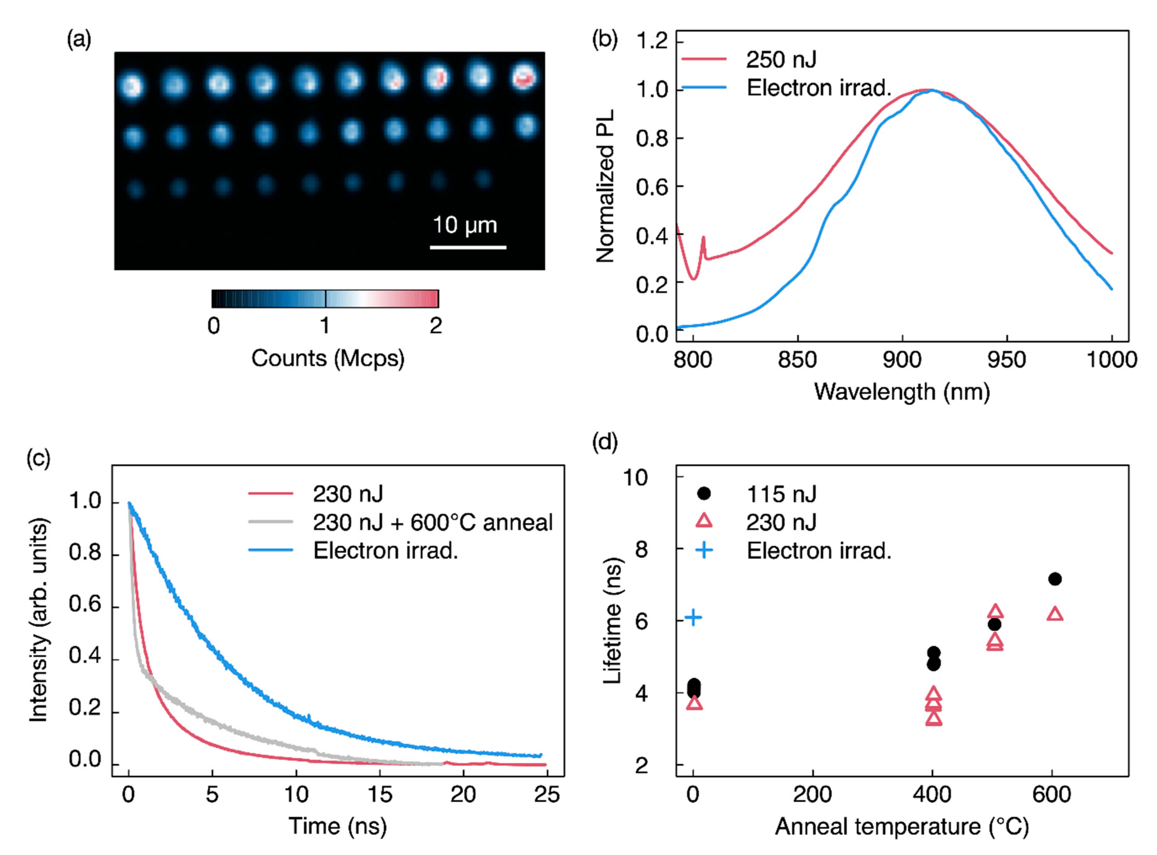
4.2.2. Semi-Insulating Unintentionally Doped 4H-SiC
5. Conclusions
Author Contributions
Funding
Data Availability Statement
Acknowledgments
Conflicts of Interest
References
- Gattass, R.R.; Mazur, E. Femtosecond laser micromachining in transparent materials. Nat. Photonics 2008, 2, 219–225. [Google Scholar] [CrossRef]
- Vanagas, E.; Kudryashov, I.; Tuzhilin, D.; Juodkazis, S.; Matsuo, S.; Misawa, H. Surface nanostructuring of borosilicate glass by femtosecond nJ energy pulses. Appl. Phys. Lett. 2003, 82, 2901–2903. [Google Scholar] [CrossRef]
- Watanabe, M.; Sun, H.; Juodkazis, S.; Takahashi, T.; Matsuo, S.; Suzuki, Y.; Nishii, J.; Misawa, H. Three-Dimensional Optical Data Storage in Vitreous Silica. Jpn. J. Appl. Phys. 1998, 37, L1527–L1530. [Google Scholar] [CrossRef]
- Juodkazis, S.; Nishimura, K.; Misawa, H.; Ebisui, T.; Waki, R.; Matsuo, S.; Okada, T. Control over the Crystalline State of Sapphire. Adv. Mater. 2006, 18, 1361–1364. [Google Scholar] [CrossRef]
- Juodkazis, S.; Nishimura, K.; Misawa, H. In-bulk and surface structuring of sapphire by femtosecond pulses. Appl. Surf. Sci. 2007, 253, 6539–6544. [Google Scholar] [CrossRef]
- Buividas, R.; Rekštytė, S.; Malinauskas, M.; Juodkazis, S. Nano-groove and 3D fabrication by controlled avalanche using femtosecond laser pulses. Opt. Mater. Express 2013, 3, 1674–1686. [Google Scholar] [CrossRef]
- Li, Z.-Z.; Wang, L.; Fan, H.; Yu, Y.-H.; Chen, Q.-D.; Juodkazis, S.; Sun, H.-B. O-FIB: Far-field-induced near-field breakdown for direct nanowriting in an atmospheric environment. Light Sci. Appl. 2020, 9, 41. [Google Scholar] [CrossRef]
- Malinauskas, M.; Farsari, M.; Piskarskas, A.; Juodkazis, S. Ultrafast laser nanostructuring of photopolymers: A decade of advances. Phys. Rep. 2013, 533, 1–31. [Google Scholar] [CrossRef]
- Jonušauskas, L.; Gailevičius, D.; Rekštytė, S.; Baldacchini, T.; Juodkazis, S.; Malinauskas, M. Mesoscale laser 3D printing. Opt. Express 2019, 27, 15205–15221. [Google Scholar] [CrossRef]
- Chen, Y.C.; Salter, P.S.; Knauer, S.; Weng, L.; Frangeskou, A.C.; Stephen, C.J.; Ishmael, S.N.; Dolan, P.R.; Johnson, S.; Green, B.L.; et al. Laser writing of coherent colour centres in diamond. Nat. Photonics 2016, 11, 77. [Google Scholar] [CrossRef]
- Rong, Y.; Cheng, K.; Ju, Z.; Pan, C.; Ma, Q.; Liu, S.; Shen, S.; Wu, B.; Jia, T. Bright near-surface silicon vacancy centers in diamond fabricated by femtosecond laser ablation. Opt. Lett. 2019, 44, 3793–3796. [Google Scholar] [CrossRef] [PubMed]
- Sotillo, B.; Bharadwaj, V.; Hadden, J.P.; Rampini, S.; Chiappini, A.; Fernandez, T.T.; Armellini, C.; Serpengüzel, A.; Ferrari, M.; Barclay, P.E.; et al. Visible to Infrared Diamond Photonics Enabled by Focused Femtosecond Laser Pulses. Micromachines 2017, 8, 60. [Google Scholar] [CrossRef]
- Barbiero, M.; Castelletto, S.; Gu, M. Multi-focal laser fabrication of nitrogen vacancy centres in a bulk diamond. OSA Contin. 2020, 3, 3416–3423. [Google Scholar] [CrossRef]
- Chen, Y.C.; Salter, P.S.; Niethammer, M.; Widmann, M.; Kaiser, F.; Nagy, R.; Morioka, N.; Babin, C.; Erlekampf, J.; Berwian’, P.; et al. Laser writing of scalable single color centers in silicon carbide. Nano Lett. 2019, 19, 2377. [Google Scholar] [CrossRef] [PubMed]
- Castelletto, S.; Almutairi, A.; Kumagai, K.; Katkus, T.; Hayasaki, Y.; Johnson, B.; Juodkazis, S.J. Photoluminescence in hexagonal silicon carbide by direct femtosecond laser writing. Opt. Lett. 2018, 43, 6077–6080. [Google Scholar] [CrossRef]
- Buividas, R.; Aharonovich, I.; Seniutinas, G.; Wang, X.; Rapp, L.; Rode, A.V.; Taniguchi, T.; Juodkazis, S. Photoluminescence from voids created by femtosecond-laser pulses inside cubic-BN. Opt. Lett. 2015, 40, 5711–5713. [Google Scholar] [CrossRef]
- Hou, S.; Birowosuto, M.D.; Umar, S.; Anicet, M.A.; Tay, R.Y.; Coquet, P.; Tay, B.K.; Wang, H.; Teo, E.H.T. Localized emission from laser-irradiated defects in 2D hexagonal boron nitride. 2D Mater. 2017, 5, 015010. [Google Scholar] [CrossRef]
- Umar, S.; Birowosuto, D.; Hou, S.; Maurice, A.; Tay, B.K.; Teo, E.; Tchernycheva, M.; Gogneau, N.; Wang, H. Light emission from localised point defects induced in GaN crystal by femtosecond-pulsed laser. Opt. Mater. Express 2018, 8, 2703. [Google Scholar] [CrossRef]
- Castelletto, S.; Boretti, A. Silicon carbide color centers for quantum applications. J. Phys. Photonics 2020, 2, 022001. [Google Scholar] [CrossRef]
- Lohrmann, A.; Johnson, B.C.; McCallum, J.C.; Castelletto, S. A review on single photon sources in silicon carbide. Rep. Prog. Phys. 2017, 80, 034502. [Google Scholar] [CrossRef]
- Aharonovich, I.; Castelletto, S.; Simpson, D.A.; Su, C.H.; Greentree, A.D.; Prawer, S. Diamond-based single-photon emitters. Rep. Prog. Phys. 2011, 74, 076501. [Google Scholar] [CrossRef]
- Castelletto, S.; Inam, F.A.; Sato, S.-I.; Boretti, A. Hexagonal boron nitride: A review of the emerging material platform for single-photon sources and the spin–photon interface. Beilstein J. Nanotechnol. 2020, 11, 740–769. [Google Scholar] [CrossRef] [PubMed]
- Zhang, G.; Cheng, Y.; Chou, J.-P.; Gali, A. Material platforms for defect qubits and single-photon emitters. Appl. Phys. Rev. 2020, 7, 031308. [Google Scholar] [CrossRef]
- Awschalom, D.D.; Hanson, R.; Wrachtrup, J.; Zhou, B.B. Quantum technologies with optically interfaced solid-state spins. Nat. Photonics 2018, 12, 516. [Google Scholar] [CrossRef]
- Seo, H.; Falk, A.L.; Klimov, P.V.; Miao, K.C.; Galli, G.; Awschalom, D.D. Quantum decoherence dynamics of divacancy spins in silicon carbide. Nat. Commun. 2016, 7, 12935. [Google Scholar] [CrossRef]
- Castelletto, S.; Johnson, B.C.; Boretti, A. Quantum Effects in Silicon Carbide Hold Promise for Novel Integrated Devices and Sensors. Adv. Opt. Mater. 2013, 1, 609–625. [Google Scholar] [CrossRef]
- Lenzini, F.; Gruhler, N.; Walter, N.; Pernice, W.H.P. Diamond as a Platform for Integrated Quantum Photonics. Adv. Quantum Technol. 2018, 1, 1800061. [Google Scholar] [CrossRef]
- Chen, Y.-C.; Griffiths, B.; Weng, L.; Nicley, S.S.; Ishmael, S.N.; Lekhai, Y.; Johnson, S.; Stephen, C.J.; Green, B.L.; Morley, G.W.; et al. Laser writing of individual nitrogen-vacancy defects in diamond with near-unity yield. Optica 2019, 6, 662–667. [Google Scholar] [CrossRef]
- Wang, S.; Ji, L.; Li, L.; Wu, Y.; Zhang, Y.; Lin, Z. Selective 6H-SiC White Light Emission by Picosecond Laser Direct Writing. Sci. Rep. 2018, 8, 1–9. [Google Scholar] [CrossRef]
- Zhang, B.; He, S.; Yang, Q.; Liu, H.; Wang, L.; Chen, F. Femtosecond laser modification of 6H–SiC crystals for waveguide devices. Appl. Phys. Lett. 2020, 116, 111903. [Google Scholar] [CrossRef]
- Reshchikov, M.A.; Morkoç, H. Luminescence properties of defects in GaN. J. Appl. Phys. 2005, 97, 061301. [Google Scholar] [CrossRef]
- Juodkazis, S.; Eliseev, P.G.; Watanabe, M.; Sun, H.-B.; Matsuo, S.; Sugahara, T.; Sakai, S.; Misawa, H. Annealing of GaN-InGaN Multi Quantum Wells: Correlation between the Bandgap and Yellow Photoluminescence. Jpn. J. Appl. Phys. 2000, 39, 393–396. [Google Scholar] [CrossRef]
- Reshchikov, M.A.; Usikov, A.; Helava, H.; Makarov, Y. Fine structure of the red luminescence band in undoped GaN. Appl. Phys. Lett. 2014, 104, 032103. [Google Scholar] [CrossRef]
- Kudrius, T.; Šlekys, G.; Juodkazis, S. Surface-texturing of sapphire by femtosecond laser pulses for photonic applications. J. Phys. D Appl. Phys. 2010, 43, 145501. [Google Scholar] [CrossRef]
- Schaffer, C.B.; Brodeur, A.; Mazur, E. Laser-induced breakdown and damage in bulk transparent materials induced by tightly focused femtosecond laser pulses. Meas. Sci. Technol. 2001, 12, 1784–1794. [Google Scholar] [CrossRef]
- Keldysh, L. Ionization in the field of a strong electromagnetic wave. J. Sov. Phys. JETP 1965, 20, 1307–1314. [Google Scholar]
- Marcinkevičius, A.; Mizeikis, V.; Juodkazis, S.; Matsuo, S.; Misawa, H. Effect of refractive index-mismatch on laser microfabrication in silica glass. Appl. Phys. A 2003, 76, 257–260. [Google Scholar] [CrossRef]
- Lagomarsino, S.; Sciortino, S.; Obreshkov, B.; Apostolova, T.; Corsi, C.; Bellini, M.; Berdermann, E.; Schmidt, C.J. Photoionization of monocrystalline CVD diamond irradiated with ultrashort intense laser pulse. Phys. Rev. B 2016, 93, 085128. [Google Scholar] [CrossRef]
- Rothschild, M.; Arnone, C.; Ehrlich, D.J. Excimer-laser etching of diamond and hard carbon films by direct writing and optical projection. J. Vac. Sci. Technol. B Microelectron. Process. Phenom. 1986, 4, 310–314. [Google Scholar] [CrossRef]
- Liu, Y.; Chen, G.; Song, M.; Ci, X.; Wu, B.; Wu, E.; Zeng, H. Fabrication of nitrogen vacancy color centers by femtosecond pulse laser illumination. Opt. Express 2013, 21, 12843–12848. [Google Scholar] [CrossRef]
- Pimenov, S.M.; Khomich, A.A.; Neuenschwander, B.; Jäggi, B.; Romano, V. Picosecond-laser bulk modification induced enhancement of nitrogen-vacancy luminescence in diamond. J. Opt. Soc. Am. B 2016, 33, B49–B55. [Google Scholar] [CrossRef]
- Kononenko, V.V.; Vlasov, I.I.; Gololobov, V.M.; Kononenko, T.V.; Semenov, T.A.; Khomich, A.A.; Shershulin, V.A.; Krivobok, V.S.; Konov, V.I. Nitrogen-vacancy defects in diamond produced by femtosecond laser nanoablation technique. Appl. Phys. Lett. 2017, 111, 081101. [Google Scholar] [CrossRef]
- Sörman, E.; Son, N.T.; Chen, W.M.; Kordina, O.; Hallin, C.; Janzén, E. Silicon vacancy related defect in 4H and 6H SiC. Phys. Rev. B 2000, 61, 2613–2620. [Google Scholar] [CrossRef]
- Fuchs, F.; Stender, B.; Trupke, M.; Simin, D.; Pflaum, J.; Dyakonov, V.; Astakhov, G.V. Engineering near-infrared single-photon emitters with optically active spins in ultrapure silicon carbide. Nat. Commun. 2015, 6, 7578. [Google Scholar] [CrossRef]
- Rühl, M.O.C.; Götzinger, S.; Krieger, M.; Weber, H.B. Controlled generation of intrinsic near-infrared color centers in 4H-SiC via proton irradiation and annealing. Appl. Phys. Lett. 2018, 113, 122102. [Google Scholar] [CrossRef]
- Ayedh, H.M.; Bobal, V.; Nipoti, R.; Hallén, A.; Svensson, B.G. Formation and Annihilation of Carbon Vacancies in 4H-SiC. Mater. Sci. Forum 2016, 858, 331–336. [Google Scholar] [CrossRef]
- Ohshima, T.; Satoh, T.; Kraus, H.; Astakhov, G.V.; Dyakonov, V.; Baranov, P.G. Creation of silicon vacancy in silicon carbide by proton beam writing toward quantum sensing applications. J. Phys. D Appl. Phys. 2018, 51, 333002. [Google Scholar] [CrossRef]
- Kraus, H.; Simin, D.; Kasper, C.; Suda, Y.; Kawabata, S.; Kada, W.; Honda, T.; Hijikata, Y.; Ohshima, T.; Dyakonov, V.; et al. Three-dimensional proton beam writing of optically active coherent vacancy spins in silicon carbide. Nano Lett. 2017, 17, 2865. [Google Scholar] [CrossRef]
- Castelletto, S.; Johnson, B.C.; Ivády, V.; Stavrias, N.; Umeda, T.; Gali, A.; Ohshima, T. A silicon carbide room-temperature single-photon source. Nat. Mater. 2014, 13, 151–156. [Google Scholar] [CrossRef]
- Son, N.T.; Carlsson, P.; ul Hassan, J.; Janzén, E.; Umeda, T.; Isoya, J.; Gali, A.; Bockstedte, M.; Morishita, N.; Ohshima, T.; et al. Divacancy in 4H-SiC. Phys. Rev. Lett. 2006, 96, 055501. [Google Scholar] [CrossRef]
- Degen, C.L.; Reinhard, F.; Cappellaro, P. Quantum sensing. Rev. Mod. Phys. 2017, 89, 035002. [Google Scholar] [CrossRef]
- Castelletto, S.; Katkus, T.; Juodkazis, S. Laser Writing of Color Centers in Silicon Carbide; SPIE Micro Nano Materials, Devices, and Applications: Bellingham, WA, USA, 2019; Volume 11201, p. 1120112. [Google Scholar]
- Son, N.T.; Stenberg, P.; Jokubavicius, V.; Abe, H.; Ohshima, T.; Hassan, J.U.; Ivanov, I.G. Energy levels and charge state control of the carbon antisite-vacancy defect in 4H-SiC. Appl. Phys. Lett. 2019, 114, 212105. [Google Scholar] [CrossRef]
- Christle, D.J.; Falk, A.L.; Andrich, P.; Klimov, P.V.; Hassan, J.U.; Son, N.T.; Janzén, E.; Ohshima, T.; Awschalom, D.D. Isolated electron spins in silicon carbide with millisecond coherence times. Nat. Mater. 2015, 14, 160–163. [Google Scholar] [CrossRef] [PubMed]
- Wang, J.-F.; Liu, Z.-H.; Yan, F.-F.; Li, Q.; Yang, X.-G.; Guo, L.; Zhou, X.; Huang, W.; Xu, J.-S.; Li, C.-F.; et al. Experimental Optical Properties of Single Nitrogen Vacancy Centers in Silicon Carbide at Room Temperature. ACS Photonics 2020, 7, 1611–1616. [Google Scholar] [CrossRef]
- Wang, J.-F.; Yan, F.-F.; Li, Q.; Liu, Z.-H.; Liu, H.; Guo, G.-P.; Guo, L.-P.; Zhou, X.; Cui, J.-M.; Wang, J.; et al. Coherent Control of Nitrogen-Vacancy Center Spins in Silicon Carbide at Room Temperature. Phys. Rev. Lett. 2020, 124, 223601. [Google Scholar] [CrossRef] [PubMed]
- Atatüre, M.; Englund, D.; Vamivakas, N.; Lee, S.-Y.; Wrachtrup, J. Material platforms for spin-based photonic quantum technologies. Nat. Rev. Mater. 2018, 3, 38–51. [Google Scholar] [CrossRef]


| nJ Per Pulse | Material | Color Centers Identified and Depth (μm) | Annealing | |
|---|---|---|---|---|
| nm | ||||
| 515 | 13 ÷ 445 | 4H-SiC | VSi 665 nm unknown (2, 4) | Before fabrication at 1000 °C |
| HPSI | ||||
| N < 1014 cm−3 | ||||
| 515 | 13 ÷ 445 | 4H-SiC | Unknown (2, 4) | Not performed |
| n-type | ||||
| N 1019 cm−3 | ||||
| 1030 | 4 ÷ 230 | GaN | RL center (0) | Not performed |
| Thin film | ||||
| unintentionally | ||||
| n-doped | ||||
| 1030 | 4 ÷ 230 | 4H-SiC | VSi (0, 5, 10) | 400, 500, and 600 °C |
| Unintentionally doped | ||||
| N 3–6 × 1015 cm−3 |
| Material | Color Centers Identified and Depth | Reference | ||||||||
|---|---|---|---|---|---|---|---|---|---|---|
| nm | TW/cm2 | nJ | nm | fs | kHz | nJ Per Pulse | (μm) | |||
| 790 | 13.4 | 12.9 | 350 | 1.4 | 250 | 1 | 6.7 ÷ 89.9 | 4H-SiC 1 | VSi 5 | [14] |
| Intrinsic | −40 | |||||||||
| 1030 | 17.7 | 68 | 729 | 0.9 | 230 | 200 | 29 ÷ 230 | 4H-SiC 2 | VSi, VcVSi | [15,52] |
| intrinsic | (0, 5, 10) | |||||||||
| 515 | 70.9 | 68 | 364 | 0.9 | 230 | 200 | 13 ÷ 445 | 4H-SiC | VSi | This work |
| HPSI | (2, 4) | |||||||||
| 515 | 70.9 | 68 | 364 | 0.9 | 230 | 200 | 13 ÷ 445 | 4H-SiC | Unknown | This work |
| n-type 3 | (2, 4) | |||||||||
| 515 | 57.5 | 22.8 | 234 | 1.4 | 230 | 200 | 9 ÷ 90 | cBN | NV | [16] |
| (10, 20) | ||||||||||
| 1030 | 16.6 | 63.8 | 729 | 0.9 | 230 | 200 | 4 ÷ 230 | GaN | RL center | This work |
| Thin film | 0 | |||||||||
| 800 | 27.6 | 74.4 | 784 | 0.6 | 140 | 80,000 | 1.6 ÷ 5.74 | GaN | RL centers | [18] |
| Thin film | 0 | |||||||||
| 790 | 26.6 | 25.6 | 350 | 1.4 | 250 | 1 | 19.6 ÷ 61.8 | Quantum | NV 5 | [10] |
| Diamond 4 | −40 | |||||||||
| 515 | 62.6 | 31.1 | 262 | 1.25 | 230 | 500 | 10 ÷ 30 | Quantum | NV 5 | [12] |
| Diamond | −25 | |||||||||
| 800 | 25.9 | 67.7 | 1020 | 0.5 | 80 | 250 | 4,000 3 | Type Ib | NV 5 | [40] |
| Diamond | (around crater) | |||||||||
| 800 | 25.9 | 13 | 566 | 0.9 | 50 | 1 | 10,000 3 | Quantum | SiV 5 | [11] |
| Diamond | (around crater) |
Publisher’s Note: MDPI stays neutral with regard to jurisdictional claims in published maps and institutional affiliations. |
© 2020 by the authors. Licensee MDPI, Basel, Switzerland. This article is an open access article distributed under the terms and conditions of the Creative Commons Attribution (CC BY) license (http://creativecommons.org/licenses/by/4.0/).
Share and Cite
Castelletto, S.; Maksimovic, J.; Katkus, T.; Ohshima, T.; Johnson, B.C.; Juodkazis, S. Color Centers Enabled by Direct Femto-Second Laser Writing in Wide Bandgap Semiconductors. Nanomaterials 2021, 11, 72. https://doi.org/10.3390/nano11010072
Castelletto S, Maksimovic J, Katkus T, Ohshima T, Johnson BC, Juodkazis S. Color Centers Enabled by Direct Femto-Second Laser Writing in Wide Bandgap Semiconductors. Nanomaterials. 2021; 11(1):72. https://doi.org/10.3390/nano11010072
Chicago/Turabian StyleCastelletto, Stefania, Jovan Maksimovic, Tomas Katkus, Takeshi Ohshima, Brett C. Johnson, and Saulius Juodkazis. 2021. "Color Centers Enabled by Direct Femto-Second Laser Writing in Wide Bandgap Semiconductors" Nanomaterials 11, no. 1: 72. https://doi.org/10.3390/nano11010072
APA StyleCastelletto, S., Maksimovic, J., Katkus, T., Ohshima, T., Johnson, B. C., & Juodkazis, S. (2021). Color Centers Enabled by Direct Femto-Second Laser Writing in Wide Bandgap Semiconductors. Nanomaterials, 11(1), 72. https://doi.org/10.3390/nano11010072