Optimising Non-Patterned MoO3/Ag/MoO3 Anode for High-Performance Semi-Transparent Organic Solar Cells towards Window Applications


 ,
, 


Abstract
1. Introduction
2. Experimental Details
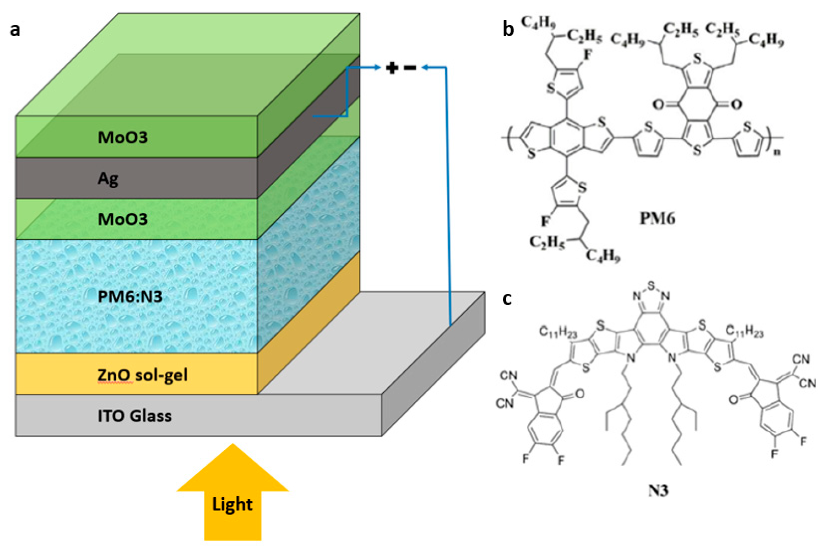
2.1. Materials Preparation
2.2. Device Fabrication
2.3. Device Characterisation
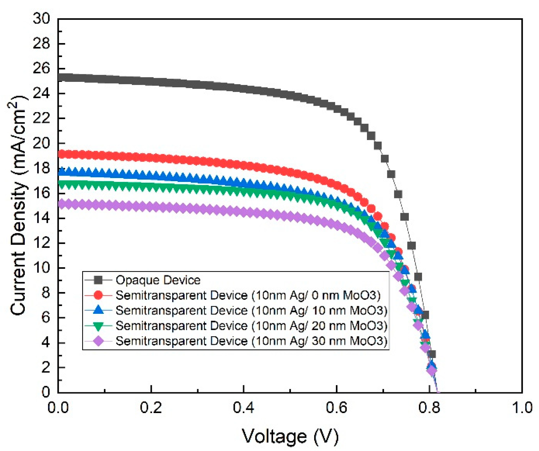
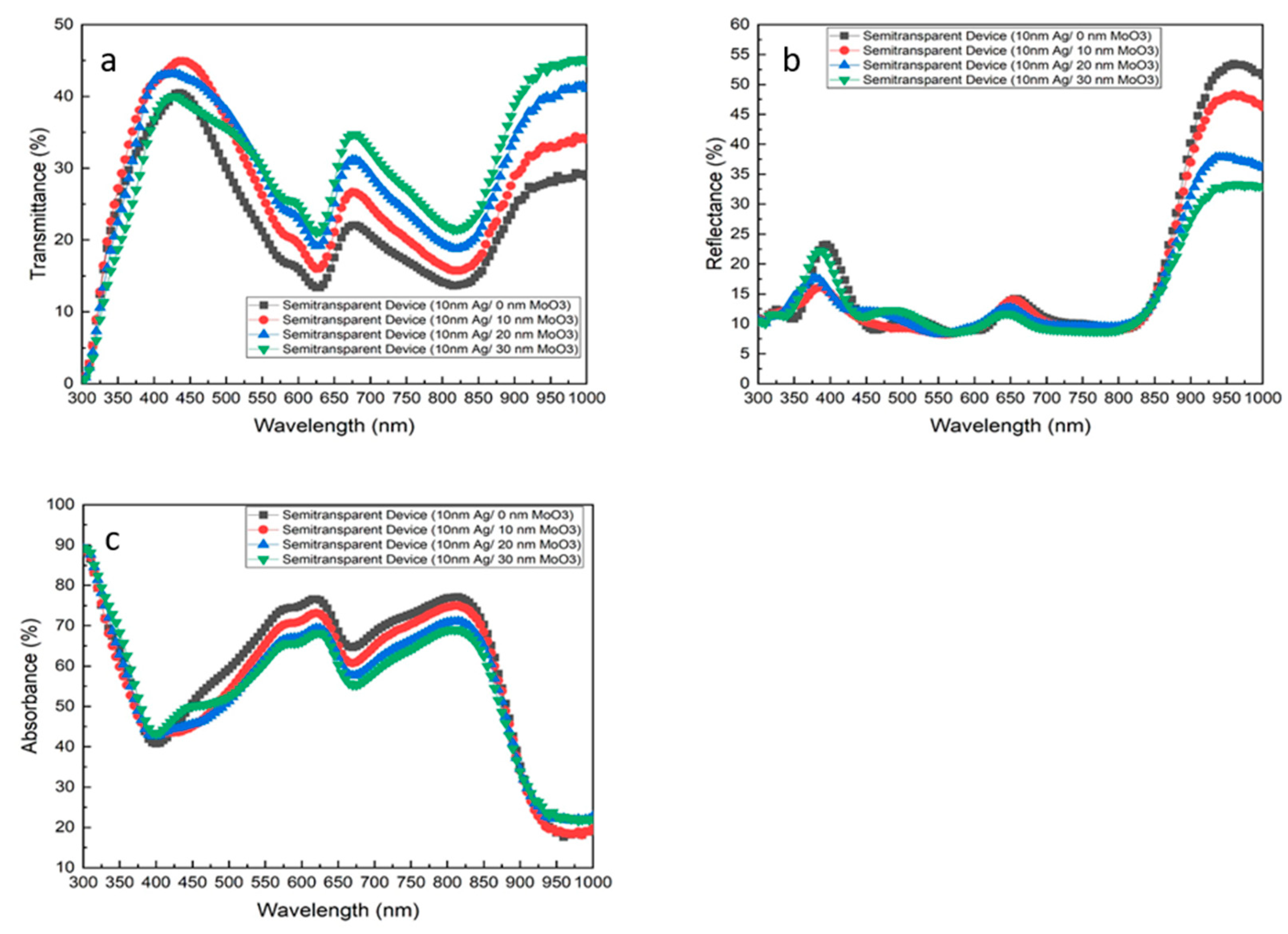
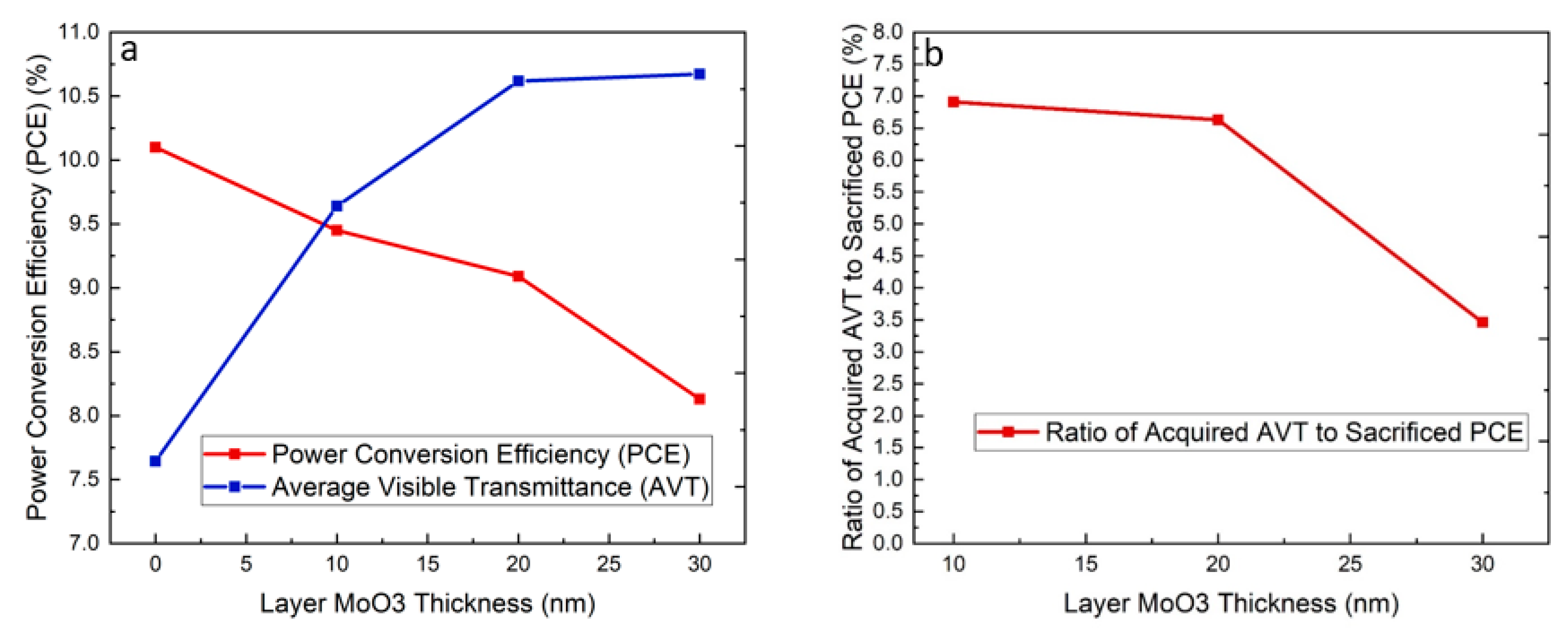
3. Results and Discussion
4. Colour Rendering Index
5. Conclusions
Author Contributions
Funding
Acknowledgments
Conflicts of Interest
References
- Guo, W.; Xu, Z.; Zhang, F.; Xie, S.; Xu, H.; Liu, X.Y. Recent development of transparent conducting Oxide-Free flexible Thin-Film solar cells. Adv. Funct. Mater. 2016, 26, 8855–8884. [Google Scholar] [CrossRef]
- Forrest, S.R. The path to ubiquitous and low-cost organic electronic appliances on plastic. Nature 2004, 428, 911–918. [Google Scholar] [CrossRef]
- Kaltenbrunner, M.; White, M.S.; Glowacki, E.D.; Sekitani, T.; Someya, T.; Sariciftci, N.S.; Bauer, S. Ultrathin and lightweight organic solar cells with high flexibility. Nat. Commun. 2012, 3, 770. [Google Scholar] [CrossRef] [PubMed]
- Duan, L.; Meng, X.; Zhang, Y.; Yi, H.; Jin, K.; Haque, F.; Xu, C.; Xiao, Z.; Ding, L.; Uddin, A. Comparative analysis of burn-in photo-degradation in non-fullerene COi8DFIC acceptor based high-efficiency ternary organic solar cells. Mater. Chem. Front. 2019, 3, 1085–1096. [Google Scholar] [CrossRef]
- Duan, L.; Uddin, A. Progress in Stability of Organic Solar Cells. Adv. Sci. 2020, 7, 1903259. [Google Scholar] [CrossRef] [PubMed]
- Duan, L.; Zhang, Y.; Yi, H.; Haque, F.; Deng, R.; Guan, H.; Zou, Y.; Uddin, A. Trade-Off between Exciton Dissociation and Carrier Recombination and Dielectric Properties in Y6-Sensitized Nonfullerene Ternary Organic Solar Cells. Energy Technol. 2019, 8, 1900924. [Google Scholar] [CrossRef]
- Wadsworth, A.; Moser, M.; Marks, A.; Little, M.S.; Gasparini, N.; Brabec, C.J.; Baran, D.; McCulloch, I. Critical review of the molecular design progress in non-fullerene electron acceptors towards commercially viable organic solar cells. Chem. Soc. Rev. 2019, 48, 1596–1625. [Google Scholar] [CrossRef]
- Liu, Q.; Jiang, Y.; Jin, K.; Qin, J.; Xu, J.; Li, W.; Xiong, J.; Liu, J.; Xiao, Z.; Sun, K. 18% Efficiency organic solar cells. Sci. Bull. 2020, 65, 272–275. [Google Scholar] [CrossRef]
- Li, Z.; Klein, T.R.; Kim, D.H.; Yang, M.; Berry, J.J.; Van Hest, M.F.A.M.; Zhu, K. Scalable fabrication of perovskite solar cells. Nat. Rev. Mater. 2018, 3, 18017. [Google Scholar] [CrossRef]
- Chen, K.-S.; Salinas, J.-F.; Yip, H.-L.; Huo, L.; Hou, J.; Jen, A.K.-Y. Semi-transparent polymer solar cells with 6% PCE, 25% average visible transmittance and a color rendering index close to 100 for power generating window applications. Energy Environ. Sci. 2012, 5, 9551–9557. [Google Scholar] [CrossRef]
- Betancur, R.; Romero-Gomez, P.; Martínez-Otero, A.; Elias, X.; Maymó, M.; Martorell, J. Transparent polymer solar cells employing a layered light-trapping architecture. Nat. Photonics 2013, 7, 995–1000. [Google Scholar] [CrossRef]
- Chang, C.Y.; Zuo, L.; Yip, H.L.; Li, C.Z.; Li, Y.; Hsu, C.S.; Cheng, Y.J.; Chen, H.; Jen, A.K.Y. Highly Efficient Polymer Tandem Cells and Semitransparent Cells for Solar Energy. Adv. Energy Mater. 2013, 4, 1301645. [Google Scholar] [CrossRef]
- Tian, X.; Zhang, Y.; Hao, Y.; Cui, Y.; Wang, W.; Shi, F.; Wang, H.; Wei, B.; Huang, W. Semitransparent inverted organic solar cell with improved absorption and reasonable transparency perception based on the nanopatterned MoO3/Ag/MoO3 anode. J. Nanophotonics 2015, 9, 093043. [Google Scholar] [CrossRef]
- Ameri, T.; Dennler, G.; Waldauf, C.; Azimi, H.; Seemann, A.; Forberich, K.; Hauch, J.; Scharber, M.; Hingerl, K.; Brabec, C.J. Fabrication, optical modeling, and color characterization of semitransparent bulk-heterojunction organic solar cells in an inverted structure. Adv. Funct. Mater. 2010, 20, 1592–1598. [Google Scholar] [CrossRef]
- Joseph, B.; Pogrebnaya, T.; Kichonge, B. Semitransparent building-integrated photovoltaic: Review on energy performance, challenges, and future potential. Int. J. Photoenergy 2019, 2019, 5214150. [Google Scholar] [CrossRef]
- Xiong, Y.; Ravishankar, E.; Swift, J.; Ade, H.; Booth, R.; Charles, M.; Henry, R.; O′Connor, B.; Rech, J.; Saravitz, C. Semi-transparent organic solar cells for greenhouse application (Conference Presentation). In Organic, Hybrid, and Perovskite Photovoltaics XX; International Society for Optics and Photonics: Bellingham, WA, USA, 2019; p. 110940N. [Google Scholar]
- Cho, J.M.; Lee, S.K.; Moon, S.-J.; Jo, J.; Shin, W.S. MoO3/Ag/MoO3 top anode structure for semitransparent inverted organic solar cells. Curr. Appl. Phys. 2014, 14, 1144–1148. [Google Scholar] [CrossRef]
- Upama, M.B.; Wright, M.; Elumalai, N.K.; Mahmud, M.A.; Wang, D.; Chan, K.H.; Xu, C.; Haque, F.; Uddin, A. High performance semitransparent organic solar cells with 5% PCE using non-patterned MoO3/Ag/MoO3 anode. Curr. Appl. Phys. 2017, 17, 298–305. [Google Scholar] [CrossRef]
- Tao, C.; Xie, G.; Liu, C.; Zhang, X.; Dong, W.; Meng, F.; Kong, X.; Shen, L.; Ruan, S.; Chen, W. Semitransparent inverted polymer solar cells with MoO3/Ag/MoO3 as transparent electrode. Appl. Phys. Lett. 2009, 95, 206. [Google Scholar] [CrossRef]
- Upama, M.B.; Mahmud, A.; Yi, H.; Elumalai, N.K.; Conibeer, G.; Wang, D.; Xu, C.; Uddin, A. Low-temperature processed efficient and colourful semitransparent perovskite solar cells for building integration and tandem applications. Org. Electron. 2019, 65, 401–411. [Google Scholar] [CrossRef]
- Guillén, C.; Herrero, J. ITO/metal/ITO multilayer structures based on Ag and Cu metal films for high-performance transparent electrodes. Sol. Energy Mater. Sol. Cells 2008, 92, 938–941. [Google Scholar] [CrossRef]
- Jeong, D.-N.; Lee, D.-K.; Seo, S.; Lim, S.Y.; Zhang, Y.; Shin, H.; Cheong, H.; Park, N.-G. Perovskite Cluster-Containing Solution for Scalable D-Bar Coating toward High-Throughput Perovskite Solar Cells. ACS Energy Lett. 2019, 4, 1189–1195. [Google Scholar] [CrossRef]
- Upama, M.B.; Wright, M.; Elumalai, N.K.; Mahmud, A.; Wang, D.; Xu, C.; Uddin, A. High-efficiency semitransparent organic solar cells with non-fullerene acceptor for window application. ACS Photonics 2017, 4, 2327–2334. [Google Scholar] [CrossRef]
- Jiang, Y.; Almansouri, I.; Huang, S.; Young, T.; Li, Y.; Peng, Y.; Hou, Q.; Spiccia, L.; Bach, U.; Cheng, Y.-B.; et al. Optical analysis of perovskite/silicon tandem solar cells. J. Mater. Chem. C 2016, 4, 5679–5689. [Google Scholar] [CrossRef]
- Yu, W.; Jia, X.; Long, Y.; Shen, L.; Liu, Y.; Guo, W.; Ruan, S. Highly efficient semitransparent polymer solar cells with color rendering index approaching 100 using one-dimensional photonic crystal. ACS Appl. Mater. Interfaces 2015, 7, 9920–9928. [Google Scholar] [CrossRef] [PubMed]
- Li, X.; Budai, J.; Liu, F.; Howe, J.Y.; Zhang, J.; Wang, X.-J.; Gu, Z.; Sun, C.; Meltzer, R.S.; Pan, Z. New yellow Ba0.93Eu0.07Al2O4 phosphor for warm-white light-emitting diodes through single-emitting-center conversion. Light Sci. Appl. 2013, 2, e50. [Google Scholar] [CrossRef]
- Yan, C.; Barlow, S.; Wang, Z.; Yan, H.; Jen, A.K.-Y.; Marder, S.R.; Zhan, X. Non-fullerene acceptors for organic solar cells. Nat. Rev. Mater. 2018, 3, 1–19. [Google Scholar] [CrossRef]
- Chen, W.; Zhang, Q. Recent progress in non-fullerene small molecule acceptors in organic solar cells (OSCs). J. Mater. Chem. C 2017, 5, 1275–1302. [Google Scholar] [CrossRef]
- Jia, B.; Wu, Y.; Zhao, F.; Yan, C.; Zhu, S.; Cheng, P.; Mai, J.; Lau, T.-K.; Lu, X.; Su, C.-J. Rhodanine flanked indacenodithiophene as non-fullerene acceptor for efficient polymer solar cells. Sci. China Ser. B Chem. 2017, 60, 257–263. [Google Scholar] [CrossRef]
- Jiang, K.; Wei, Q.; Lai, J.Y.L.; Peng, Z.; Kim, H.K.; Yuan, J.; Ye, L.; Ade, H.; Zou, Y.; Yan, H. Alkyl chain tuning of small molecule acceptors for efficient organic solar cells. Joule 2019, 3, 3020–3033. [Google Scholar] [CrossRef]
- Yuan, J.; Zhang, Y.; Zhou, L.; Zhang, G.; Yip, H.-L.; Lau, T.-K.; Lu, X.; Zhu, C.; Peng, H.; Johnson, P.A. Single-junction organic solar cell with over 15% efficiency using fused-ring acceptor with electron-deficient core. Joule 2019, 3, 1140–1151. [Google Scholar] [CrossRef]
- Duan, L.; Zhang, Y.; He, M.; Deng, R.; Yi, H.; Wei, Q.; Zou, Y.; Uddin, A. Burn-In Degradation Mechanism Identified for Small Molecular Acceptor-Based High-Efficiency Nonfullerene Organic Solar Cells. ACS Appl. Mater. Interfaces 2020, 12, 27433–27442. [Google Scholar] [CrossRef] [PubMed]
- Duan, L.; Yi, H.; Wang, Z.; Zhang, Y.; Haque, F.; Sang, B.; Deng, R.; Uddin, A. Semitransparent organic solar cells based on PffBT4T-2OD with a thick active layer and near neutral colour perception for window applications. Sustain. Energy Fuels 2019, 3, 2456–2463. [Google Scholar] [CrossRef]
- Street, R.A.; Schoendorf, M.; Roy, A.; Lee, J.H. Interface state recombination in organic solar cells. Phys. Rev. B 2010, 81, 205307. [Google Scholar] [CrossRef]
- Brus, V.V.; Lee, J.; Luginbuhl, B.R.; Ko, S.J.; Bazan, G.C.; Nguyen, T.Q. Solution-Processed Semitransparent Organic Photovoltaics: From Molecular Design to Device Performance. Adv. Mater. 2019, 31, 1900904. [Google Scholar] [CrossRef]
- Yang, D.; Sano, T.; Sasabe, H.; Yang, L.; Ohisa, S.; Chen, Y.; Huang, Y.; Kido, J. Colorful squaraines dyes for efficient solution-processed all small-molecule semitransparent organic solar cells. ACS Appl. Mater. Interfaces 2018, 10, 26465–26472. [Google Scholar] [CrossRef]
- Li, Y.; Xu, G.; Cui, C.; Li, Y. Flexible and semitransparent organic solar cells. Adv. Energy Mater. 2017, 8, 1701791. [Google Scholar] [CrossRef]
- Colsmann, A.; Puetz, A.; Bauer, A.; Hanisch, J.; Ahlswede, E.; Lemmer, U. Efficient semi-transparent organic solar cells with good transparency color perception and rendering properties. Adv. Energy Mater. 2011, 1, 599–603. [Google Scholar] [CrossRef]
- Romero-Gomez, P.; Betancur, R.; Martinez-Otero, A.; Elias, X.; Mariano, M.; Romero, B.; Arredondo, B.; Vergaz, R.; Martorell, J. Enhanced stability in semi-transparent PTB7/PC71BM photovoltaic cells. Sol. Energy Mater. Sol. Cells 2015, 137, 44–49. [Google Scholar] [CrossRef][Green Version]


| Devices | Voc (V) | Jsc (mA/cm2) | FF(%) | PCE(%) | Rs (Ω) | Rsh (Ω) |
|---|---|---|---|---|---|---|
| Opaque Device (100 nm Ag/0 nm MoO3) | 0.82 ± 0.00 | 25.29 ± 0.71 | 66.91 ± 1.40 | 13.79 ± 0.34 | 131 ± 18 | 18,444 ± 822 |
| Semi-transparent Device (10 nm Ag/0 nm MoO3) | 0.80 ± 0.00 | 19.15 ± 0.31 | 64.92 ± 1.10 | 9.96 ± 0.10 | 144 ± 9 | 18,511 ± 3111 |
| Semi-transparent Device (10 nm Ag/10 nm MoO3) | 0.79 ± 0.00 | 17.68 ± 0.45 | 65.41 ± 0.45 | 9.18 ± 0.23 | 147 ± 4 | 19,200 ± 1244 |
| Semi-transparent Device (10 nm Ag/20 nm MoO3) | 0.81 ± 0.00 | 16.79 ± 0.17 | 65.46 ± 1.79 | 8.86 ± 0.20 | 191 ± 24 | 25,089 ± 1822 |
| Semi-transparent Device (10 nm Ag/30 nm MoO3) | 0.80 ± 0.01 | 15.15 ± 0.53 | 64.67 ± 2.70 | 7.84 ± 0.19 | 207 ± 24 | 23,333 ± 4933 |
| Devices | AVT |
| Opaque Device | 0.00% |
| Semitransparent Device (10 nm Ag/0 nm MoO3) | 24.45% |
| Semitransparent Device (10 nm Ag/10 nm MoO3) | 28.94% |
| Semitransparent Device (10 nm Ag/20 nm MoO3) | 31.14% |
| Semitransparent Device (10 nm Ag/30 nm MoO3) | 31.26% |
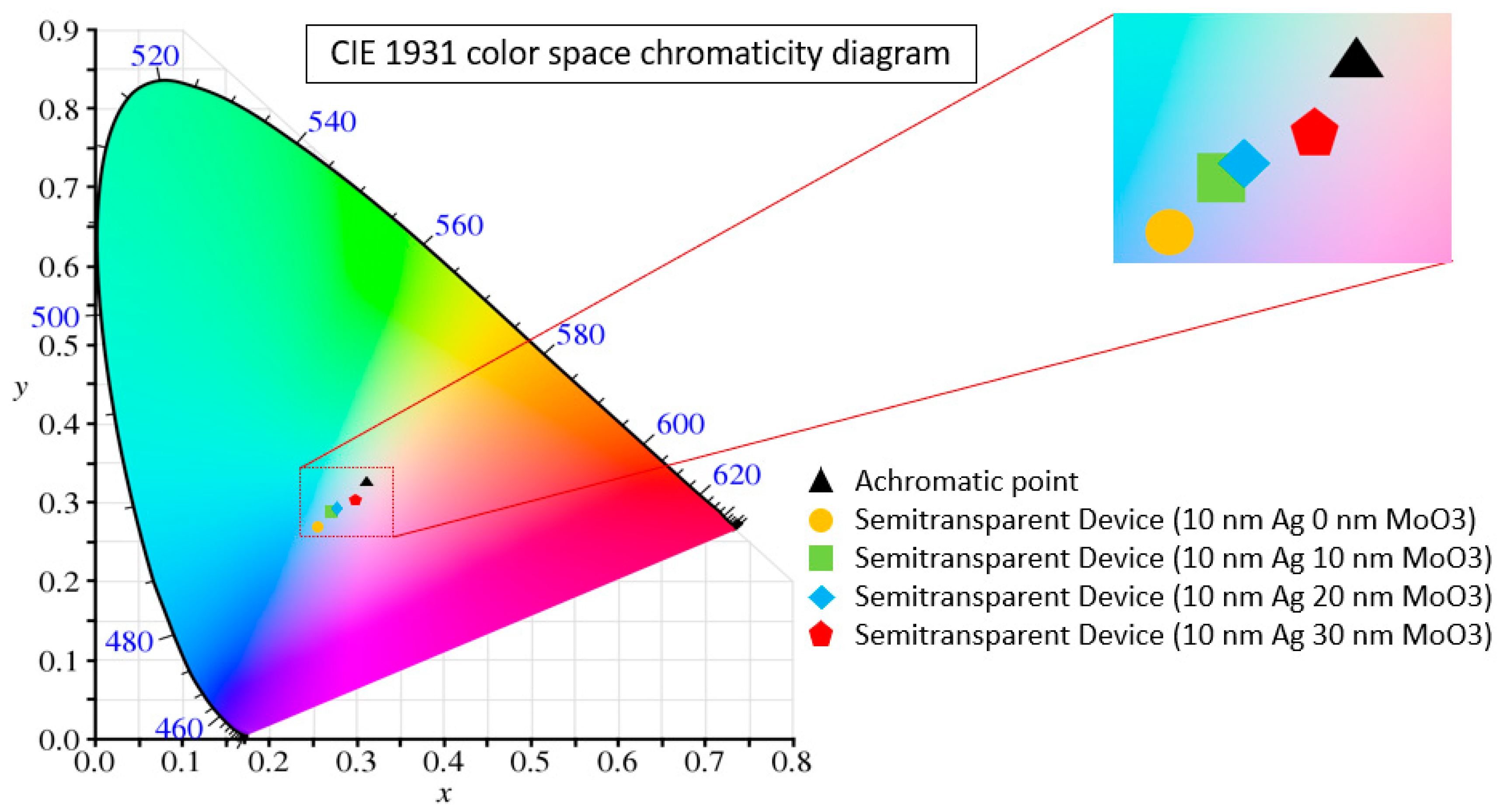
| Devices | x | y | CRI |
|---|---|---|---|
| Semitransparent Device (10 nm Ag/0 nm MoO3) | 0.2536 | 0.2692 | 97.3 |
| Semitransparent Device (10 nm Ag/10 nm MoO3) | 0.2702 | 0.2843 | 97.0 |
| Semitransparent Device (10 nm Ag/20 nm MoO3) | 0.2828 | 0.2942 | 95.4 |
| Semitransparent Device (10 nm Ag/30 nm MoO3) | 0.2994 | 0.3039 | 92.1 |
© 2020 by the authors. Licensee MDPI, Basel, Switzerland. This article is an open access article distributed under the terms and conditions of the Creative Commons Attribution (CC BY) license (http://creativecommons.org/licenses/by/4.0/).
Share and Cite
Chang, L.; Duan, L.; Sheng, M.; Yuan, J.; Yi, H.; Zou, Y.; Uddin, A. Optimising Non-Patterned MoO3/Ag/MoO3 Anode for High-Performance Semi-Transparent Organic Solar Cells towards Window Applications. Nanomaterials 2020, 10, 1759. https://doi.org/10.3390/nano10091759
Chang L, Duan L, Sheng M, Yuan J, Yi H, Zou Y, Uddin A. Optimising Non-Patterned MoO3/Ag/MoO3 Anode for High-Performance Semi-Transparent Organic Solar Cells towards Window Applications. Nanomaterials. 2020; 10(9):1759. https://doi.org/10.3390/nano10091759
Chicago/Turabian StyleChang, Lichun, Leiping Duan, Ming Sheng, Jun Yuan, Haimang Yi, Yingping Zou, and Ashraf Uddin. 2020. "Optimising Non-Patterned MoO3/Ag/MoO3 Anode for High-Performance Semi-Transparent Organic Solar Cells towards Window Applications" Nanomaterials 10, no. 9: 1759. https://doi.org/10.3390/nano10091759
APA StyleChang, L., Duan, L., Sheng, M., Yuan, J., Yi, H., Zou, Y., & Uddin, A. (2020). Optimising Non-Patterned MoO3/Ag/MoO3 Anode for High-Performance Semi-Transparent Organic Solar Cells towards Window Applications. Nanomaterials, 10(9), 1759. https://doi.org/10.3390/nano10091759