Article

Multi-Channel Exploration of O Adatom on TiO2(110) Surface by Scanning Probe Microscopy

1
Key Laboratory of Instrumentation Science and Dynamic Measurement, School of Instrument and Electronics, North University of China, Taiyuan 030051, China
2
Department of Applied Physics, Graduate School of Engineering, Osaka University, 2-1 Yamadaoka, Suita, Osaka 565-0871, Japan
*
Author to whom correspondence should be addressed.
Nanomaterials 2020, 10(8), 1506; https://doi.org/10.3390/nano10081506
Submission received: 8 July 2020 / Revised: 22 July 2020 / Accepted: 29 July 2020 / Published: 31 July 2020
(This article belongs to the Special Issue Characterization of Nanocrystalline Materials)

Abstract

:
We studied the O2 dissociated state under the different O2 exposed temperatures with atomic resolution by scanning probe microscopy (SPM) and imaged the O adatom by simultaneous atomic force microscopy (AFM)/scanning tunneling microscopy (STM). The effect of AFM operation mode on O adatom contrast was investigated, and the interaction of O adatom and the subsurface defect was observed by AFM/STM. Multi-channel exploration was performed to investigate the charge transfer between the adsorbed O and the TiO2(110) by obtaining the frequency shift, tunneling current and local contact potential difference at an atomic scale. The tunneling current image showed the difference of the tunneling possibility on the single O adatom and paired O adatoms, and the local contact potential difference distribution of the O-TiO2(110) surface institutively revealed the charge transfer from TiO2(110) surface to O adatom. The experimental results are expected to be helpful in investigating surface/interface properties by SPM.

1. Introduction

Scanning probe microscopy (SPM) has developed as a powerful tool for exploring the surface properties and surface dynamic process at an atomic scale on a semiconductor or insulator [1,2,3,4,5,6,7,8,9,10]. For example, atomic manipulation has been realized, and surface chemical reactions have been observed with atomic resolution by atomic force microscopy (AFM). Based on AFM, Kelvin probe force microscopy (KPFM) was developed to characterize the contact potential difference (CPD) between the substrate and cantilever tip. CPD originates from the difference of the work functions and is specifically referred to as the local CPD (LCPD) in atomic-resolution KPFM [11,12]. To date, different modes of KPFM have been successfully used to simultaneously measure surface structures and LCPD, and the surface potential of TiO2(110) was measured [13,14,15,16,17,18,19]. Local density of states (LDOS) gives significant information of the electronic structure of the surface, which is measured by scanning tunneling microscopy (STM). Combining AFM/STM techniques has been developed to investigate the surface structure and LDOS [20,21,22]. Simultaneous measurement of tunneling current and LCPD is useful to explore the surface properties and surface reaction process, but it cannot be achieved by the conventional KPFM due to the regulation of DC bias voltage. To simultaneously characterize the electronic structure and LCPD, we previously proposed a method to achieve the frequency shift (∆f), average tunneling current (<It>) and LCPD by the KPFM without DC bias voltage feedback, and this method was successfully performed on the rutile TiO2(110) surface [19]. Hence, based on AFM, multi-channel exploration has the potential to explore the charge transfer of the interface and to unravel physical features for understanding the surface catalytic process.
Oxygen molecular interaction with TiO2 has attracted much attention and has become a prototypical model due to its importance in many surface reactions. Molecular oxygen acts as the main oxidizing reagent in many catalytic reactions and is used as an electron scavenger, which is believed to facilitate surface reactions. The adsorption and dissociation of O2 on the rutile TiO2(110) surface at low and room temperatures have been well characterized by STM experimental and theoretical study, where the oxygen molecular adsorbed on the Ti5c site or the surface bridging oxygen vacancies (Ov) and the oxygen adatom (Oad) along the fivefold-coordinated Ti5c site is formed [23,24]. Importantly, it is believed that chemical adsorption and dissociation of O2 on the TiO2 surface accompanied by the charge transfer and the activation of O2 dissociation are key factors in the reaction process, which is importantly related to their charge state. Therefore, multi-channel exploring of the state of Oad on TiO2(110) surface is useful in understanding its fundamental mechanism.
In this study, we first showed the dissociation state of Oad on the TiO2(110) surface under the different O2-exposed temperatures by AFM, and then we characterized the Oad by simultaneous AFM/STM, which would provide complementary information in recording the topographic and tunneling current signals. Finally, simultaneous measurements of frequency shift, tunneling current and LCPD images on the O-TiO2(110) surface are taken by SPM. The tunneling current contrast and surface potential difference were analyzed to explore the charge transfer between the Oad and TiO2 surface. The experimental results and methods are useful in characterizing the other nanomaterials.

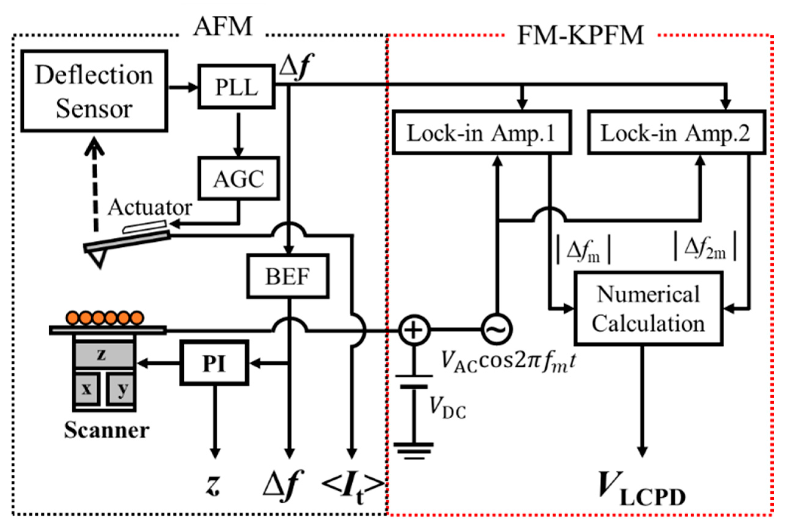
2. Experimental Details

Experiments were performed with a home-built no contact (NC)-AFM system under ultrahigh vacuum conditions (3 × 10⁻¹¹ Torr) at 78 K, which was operated in frequency modulation (FM). An AFM cantilever was oscillated at a constant amplitude and at its resonant frequency by automatic gain control (AGC). AFM/STM simultaneous measurements can be carried out in two ways, and force signal and tunneling current are recorded in the separated channel. When the frequency shift was operated as the feedback signal, topographic and <It> images were simultaneously recorded and <It> contained crosstalk of tip motion. When measurements were taken in the constant height mode, frequency shift and <It> could be simultaneously obtained. In this mode, two signals were independently measured, so they did not contain the artificial signal. The comparison of two operation modes will be shown in the results section. Figure 1 shows the experimental setup for simultaneous measurements of topography, <It> and LCPD. Topography and <It> images were obtained by AFM, and LCPD images were recorded by FM-KPFM in the constant height mode. The equation for VLCPD was derived as follows; details can be found in Ref. [18,19]:
V LCPD = V DC sgn ( α m ) V ac 4 | Δ f m | | Δ f 2 m | T ( f 2 m ) T ( f m )
Here, VDC is the dc voltage. The parameter sgn(αm) is known by the phase difference between Vac and |∆fm|. |∆fm| and |∆f2m| are the fm and f2m components of ∆f, respectively. The T(fm) and T(f2m) are the transfer functions of the phase-locked-loop (PLL).
The signal frequency shift was obtained by the phase locked loop (PLL) and divided into two parts. One was applied to adjust the tip–sample interaction with a band elimination filter (BEF), and the other was connected to FM-KPFM by feeding it into the lock-in amplifiers. An ac bias voltage was obtained by an oscillator and acted as the reference signal. The fm and f2m components of the frequency shift were detected by two lock-in amplifiers. As shown in Figure 1, <It> was recorded in a separate channel from the tip to cancel the crosstalk, and bias voltage was applied to the sample.
The commercial Ir-coated cantilever (Nanosensors SD-T10L100, f0 ~800 kHz) was used in the current study. The cantilever tip was first degassed at approximately 650 K for 30 min and then cleaned by Ar ion bombardment to remove the contaminants, prior to the measurements. Features of the surface structure were related to the charge states of the tip apex, and a stable tip was essential to accurately characterize the surface structure and properties in the experiment [25,26]. The imaging mode became stable in AFM experiments when the metal-coated Si cantilever was employed in the experiments [27,28,29].
The TiO2(110) sample surface (provided by Furuuchi Chemical Corporation, Hyogo, Japan) was prepared by several cycles of Ar ion sputtering and subsequent annealing at 1000 K for 20 min. After that, the freshly cleaned surface was exposed to O2 in the preparation chamber and then transferred into the observation chamber. AFM images were taken after the sample temperature decreased to 78 K.

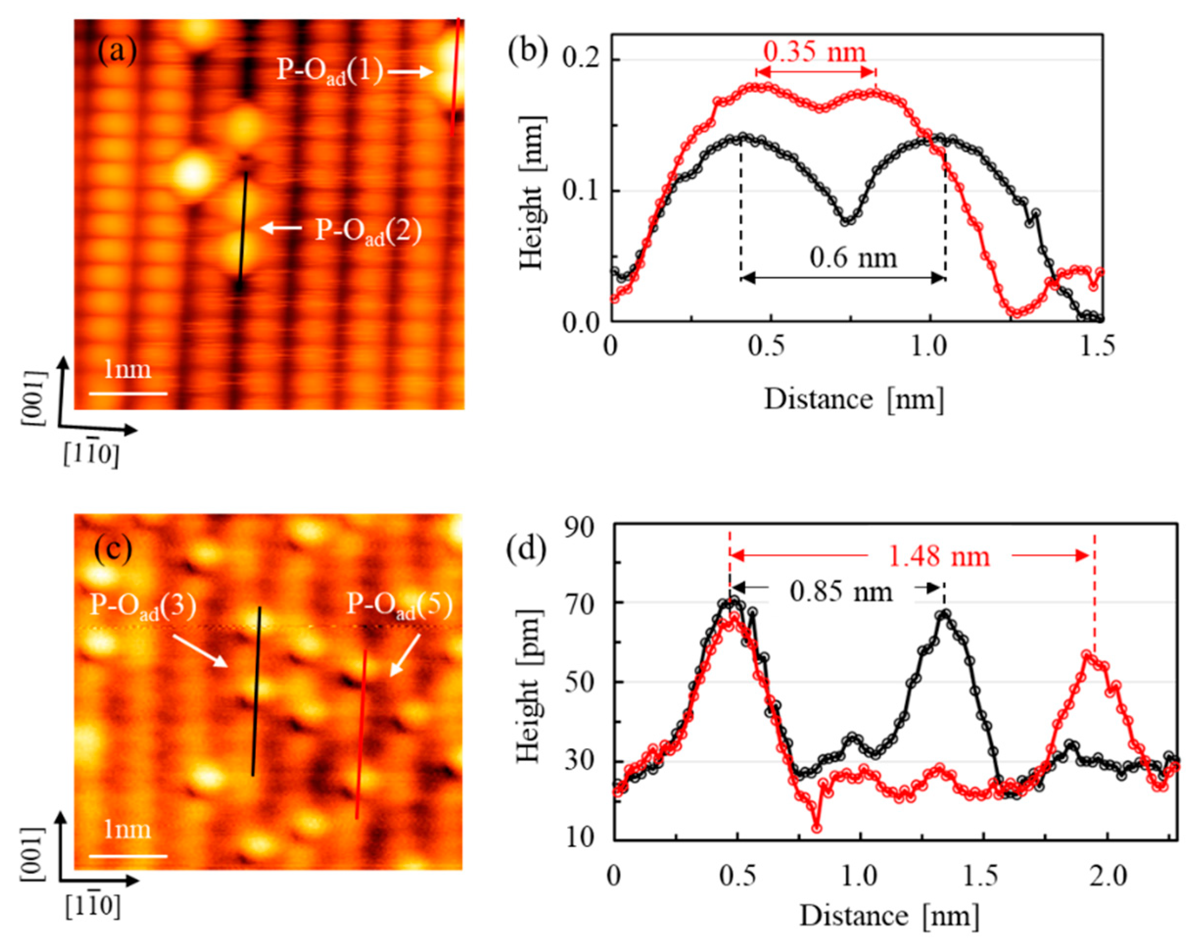
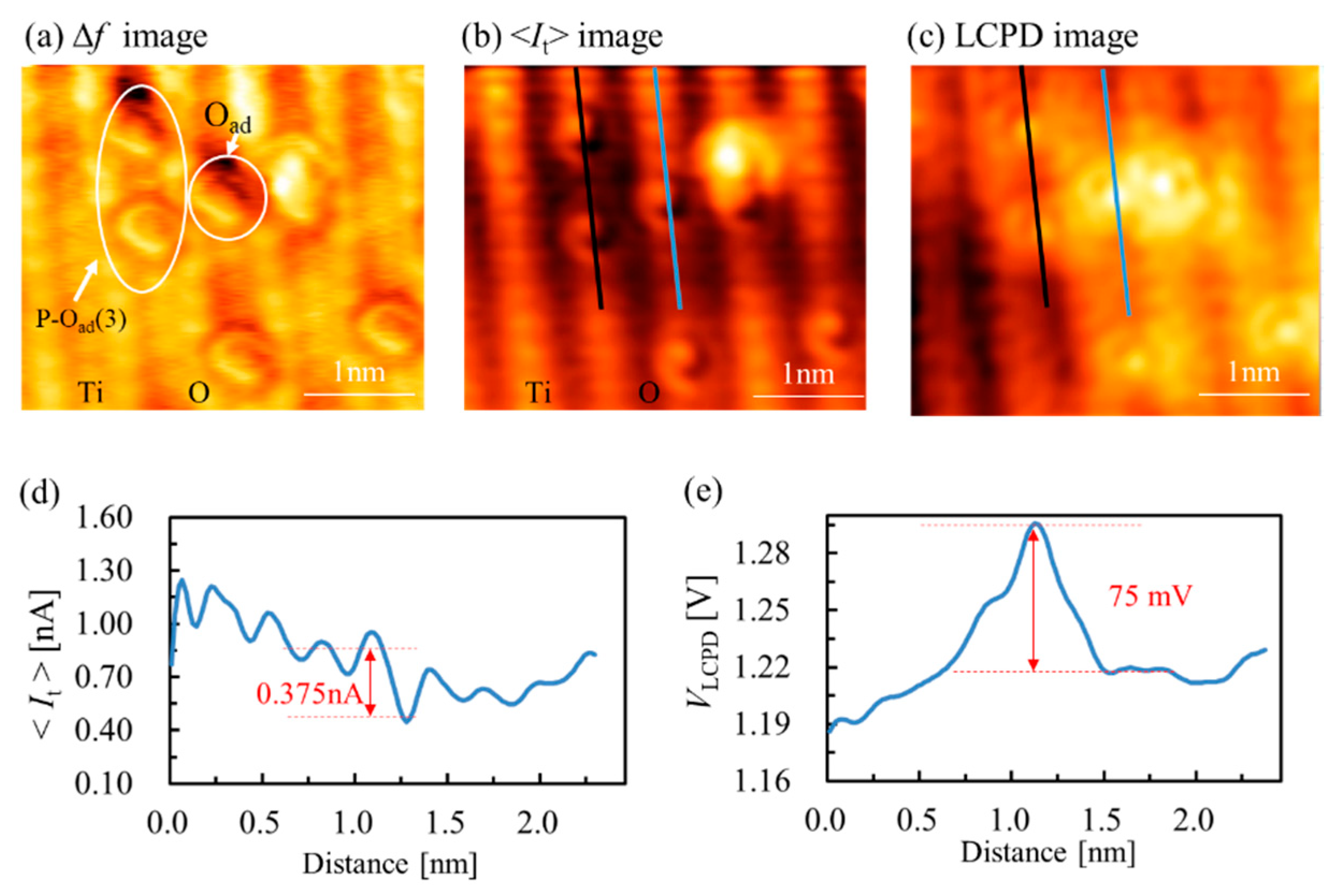
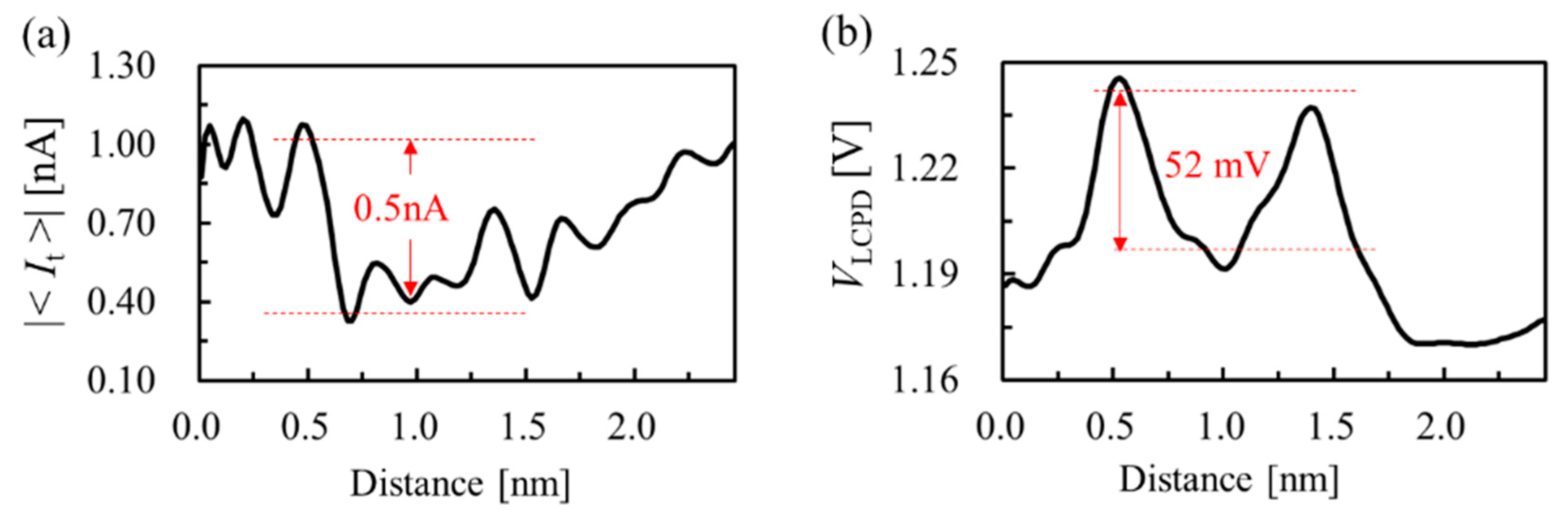
3. Results and Discussion

We first introduced the surface structure model of rutile O-TiO2 (110)-(1 × 1) and O2 dissociation state at room temperature (RT) and 400 K. Figure 2a shows a ball model of the rutile O-TiO2 (110)-(1 × 1) surface, which consists of alternating Ti5c rows and sixfold-coordinated Ti6c rows surrounded by in-plane threefold-coordinated O3c rows and bridging twofold-coordinated O2c rows. The single Oad (Oad: light green ball) formed by O2 dissociation at the Ov site indicated that one O atom healed Ov and the other located at the Ti5c site, and paired Oad resulted from O2 dissociation at the Ti5c site.
As reported in the previous literature [30,31,32], atomic contrast in the AFM image depended on the tip apex polarity, and surface defects were used as markers to distinguish the imaging mode. Hole and protrusion modes usually appeared in the imaging modes. When the tip apex was positively charged, the O2c row was bright on the image due to the larger attractive force between the tip and the negative O2c row. Surface defects were imaged as dark holes, which is called the hole mode [28,29]. When the tip apex was negatively charged, the contrast was inverted compared with that in the hole mode, and H atoms appeared as brighter spots than the OV defects, which is called the protrusion mode. Figure 2b shows the topography image of the O-TiO2(110)-(1 × 1) surface recorded in the hole mode. According to the experiment, bridging O2c and Ti5c rows were imaged as bright and dark features, respectively, and the bright spots on the Ti5c rows are Oad. As introduced before, the single Oad (denoted by the white dotted circle) was attributed to O2 dissociation at the Ov site, and paired Oad separated by three lattice distances (denoted by the white dotted oval circle) was the result of O2 dissociation at the Ti5c site.
Figure 3 shows two AFM topographic images of the rutile O-TiO2(110)-(1 × 1) surface exposed to O2 at RT and 400 K, respectively, and the corresponding line profiles along the Oad. The contrast is the same as Figure 2b. O2c and Ti5c rows are imaged as bright and dark features, respectively, and the bright spots on the Ti5c rows are Oad. Here, paired Oad separated by one lattice constant is denoted as the P-Oad(1). As shown in Figure 3a,b and Figure 2b, single Oad, P-Oad(1), P-Oad(2) and P-Oad(3) are observed when O2 is exposed to the TiO2 surface at room temperature (RT). As introduced before, single Oad was attributed to O2 dissociation at the Ov site, and paired Oad was the result of O2 dissociation at the Ti5c site. In our results, a single O adatom was the distinctly dominant state of Oad, when the exposure temperature was at RT. P-Oad(2) is the second preferred state. Density functional theory (DFT) showed the P-Oad(2) configuration was the most preferred structure at RT, and further Oad diffusion (P-Oad(2) to P-Oad(3)) was hindered by a barrier of 1.3 eV [24]. In addition, the separation of P-Oad(1) to P-Oad(2) was exothermic by 0.4 eV theoretically. P-Oad(1) and P-Oad(3) configurations were observed in our experiments, but they were rare because separation of Oad is the result of a balance between Coulombic repulsion of two Oad and is thermally driven, and P-Oad(1) and P-Oad(3) configurations can be generated.
When the sample was exposed to O2 conditions beyond 350 K, dissociated O2 could overcome the diffusion barrier forming the P-Oad(3) structure [33]. The number of paired Oad distinctly increased on the O2-exposed surface at 400 K, and the states of the paired Oad were mainly P-Oad(3) and P-Oad(5) configurations, shown in Figure 3c,d. Under high temperatures for the O2-exposed surface (>400 K), the Ti interstitials (Tiint) can diffuse from the bulk to the near-surface region via an interstitial diffusion mechanism [34]. The concentration and distribution of Tiint in the near-surface region can vary significantly, depending on the level of bulk reduction. Current experiments suggest that the excess charge on these paired Oad is mainly provided by the Tiint rather than Ov in determining the adsorption behavior when the O2-exposed surface temperatures went beyond 400 K. Our results demonstrate that O2 dissociatively adsorbed on the rutile TiO2(110)-(1 × 1) surface when the temperature of O2 exposure was at or beyond RT, and results are consistent with the conventional STM observations [24,33]. Next, we explored the Oad on TiO2 surface by AFM/STM.
The four images in Figure 4 are obtained in the same area of the O-TiO2(110) surface. Figure 4a and 4b experimentally show simultaneously recorded topographic (Z) and <It> images recorded in the constant frequency shift mode. In the topographic image (Figure 4a), the atomic contrast is the same as that in Figure 3a, in that the bright and dark rows are the O2c and Ti5c rows, respectively. A bright spot marked by the dashed white circle is Oad. Figure 4b demonstrates the corresponding tunneling current image. Usually, the empty state is imaged at positive sample bias voltage in STM, so O2c and Ti5c rows are imaged as dark and bright rows, respectively, where the contrast of O2c and Ti5c rows is reversed compared with the topographic image. The dark spot marked by the white dashed circle is Oad, and this is different from the conventional STM image of O-TiO2(110), which is caused by the crosstalk of tip motion. When the tip moves on the Oad site, the additional attractive force acts in the tip–sample interaction, and the tip has to retract in order to keep a constant frequency shift. Thus, tunneling current dramatically decreases, and the contrast of Oad becomes a dark spot in <It> image. The bright spot marked by an oval circle is due to subsurface defects, which was not probed in Figure 4a, ever reported by our group or other groups [19,22]. Figure 4c is the ∆f image and Figure 4d is the corresponding tunneling current image, recorded in the constant height mode. Compared with Figure 4a,b, the image contrast is the same, except the Oad in Figure 4d. Oad is imaged as bright spot in the <It> image due to elimination of the crosstalk between topography and <It> signals in the constant height mode. A bright spot and two weak bright spots (denoted by the white square) are observed in Figure 4d, and they are Oad and subsurface defects. It indicates the subsurface defect is not repulsive to Oad. Therefore, AFM/STM is a useful technique to investigate the interaction of the adsorbate and substrate, and constant height operation is necessary. Next, we investigated the Oad by AFM/STM/KPFM.
Figure 5 shows frequency shift, tunneling current and local contact potential difference images with atomic resolution and corresponding line profiles along the single Oad. In the experiment, the measurement was performed in the constant height mode to prevent crosstalk between the signals of the frequency shift and tunneling current. In the Δf image shown in Figure 5a, O2c and Ti5c rows are simultaneously observed as bright rows with super high resolution, and Oad is imaged as the bright spot. In the <It> image (see Figure 5b), the contrast was the same as in Figure 5a, except O rows are imaged as dark, which is consistent with the previous studies by conventional STM in that the conduction band of TiO2 is dominated by Ti 3d states, and bright features are usually assigned to the empty Ti 3d states of Ti5c ions under positive sample bias voltage, even though they lie lower than the bridging O2c rows [35]. The tunneling current value on Oad was higher than that on the Ti5c rows, and the current difference between the Oad and Ti5c row was about 0.375 nA. The contrast in STM images depends on the different contributions of Ti 3d and O 2p states and their different decay as a function of the tip–sample separation [36]. Oad is higher than O2c and Ti5c rows in surface geometry, and Oad finally appeared as bright on the image. It was clearly observed that there was some depression around the Oad, and this was due to the decreased numbers of empty states near the conduction band for tunneling, which resulted from the negatively charged Oad [24]. This phenomenon was more pronounced in paired Oad, as shown in the following tunneling current line profile. In the VLCPD image (see Figure 5c), the imaging contrast was the reverse of that in the image, except for the Oad. The relative value of VLCPD between the Ti5c and O2c sites was approximately 28 mV from the line profile (not shown here), and this was in good agreement with our previous studies [18,19]. VLCPD had a higher value on the Oad than on the proximate Ti5c rows, and the relative value of CPD between the Oad and Ti5c row was about 75 mV. It intuitively suggests the electrons transferred from TiO2 to Oad.
As shown in Figure 6, line profiles are plotted along the paired Oad. The current difference between the Oad and adjacent Ti5c row was about 0.5 nA. The depression between the paired Oad was very pronounced due to the combined effect in the corresponding line profile. The surface potential distribution was also different around the single O adatom and paired Oad. The potential difference was 52 mV, as shown in Figure 6b. This indicates the charge state of Oad is different, and excess electrons around the paired Oad are shared by the paired Oad resulting in that the relative value of CPD between the Oad and Ti5c row is lower. Therefore, multi-channel exploration demonstrates the powerful ability to explore surface properties with SPM.

4. Conclusions

We studied the O2 dissociated state under different O2-exposed sample surfaces with high resolution, and we investigated the electron charge transfer between the adsorbed O and TiO2 substrate with multi-channel exploration. We observed the interaction between Oad and the subsurface, and we confirmed the electron charge transfer from the TiO2 surface to the adsorbed O upon O2 dissociation on the TiO2(110) surface by tunneling current and local contact potential difference. Our results demonstrated that multi-channel exploration was able to obtain the surface structures and charge transfers between the adsorbate and substrate, and this is expected to be useful for investigating the surface properties and charge transfer phenomena at the interface.

Author Contributions

Conceptualization and methodology, H.F.W., Y.S. and Y.J.L.; investigation, H.F.W.; data curation, H.F.W.; writing—original draft preparation, H.F.W.; writing—review and editing, H.F.W.; supervision, Y.S. and Y.J.L.; project administration, H.F.W. and Y.J.L.; funding acquisition, H.F.W. and Y.J.L. All authors have read and agreed to the published version of the manuscript.

Funding

This research is supported by Osaka University’s International Joint Research Promotion Program (J171013014, J171013007 and Ja19990011), National Key Research and Development Program of China (2017YFE0130200, 2018YFF01012502), and National Science Foundation of China (51727808, 61727804, 61874100, 51905500). This work was also supported by Natural Science Foundation of Shanxi Province of China (201901D211253, 201901D111011(ZD)) and Scientific and Technological Innovation Programs of Higher Education Institutions in Shanxi (STIP 2019L0582).

Acknowledgments

The authors would like to thank colleagues from North University of China and Osaka University for providing good suggestions regarding the manuscript.

Conflicts of Interest

The authors declare no conflict of interest.

References

  1. Sugimoto, Y.; Pou, P.; Custance, O.; Jelinek, P.; Abe, M.; Perez, R.; Morita, S. Complex patterning by vertical interchange atom manipulation using atomic force microscopy. Science 2008, 322, 413–417. [Google Scholar] [CrossRef] [PubMed]
  2. Gross, L.; Mohn, F.; Moll, N.; Liljeroth, P.; Meyer, G. The chemical structure of a molecule resolved by atomic force microscopy. Science 2009, 325, 1110–1114. [Google Scholar] [CrossRef] [PubMed] [Green Version]
  3. Zhang, J.; Chen, P.C.; Yuan, B.K.; Ji, W.; Cheng, Z.; Qiu, X.H. Real-space identification of intermolecular bonding with atomic force microscopy. Science 2013, 342, 611–614. [Google Scholar] [CrossRef] [PubMed] [Green Version]
  4. Guo, J.; Meng, X.Z.; Chen, J.; Peng, J.B.; Sheng, J.M.; Li, X.Z.; Xu, L.M.; Shi, J.R.; Wang, E.G.; Jiang, Y. Real-space imaging of interfacial water with submolecular resolution. Nat. Mater. 2014, 13, 184–189. [Google Scholar] [CrossRef] [PubMed]
  5. Bamidele, J.; Lee, S.H.; Kinoshita, Y.; Turansky, R.; Naitoh, Y.; Li, Y.J.; Sugawara, Y.; Stich, I.; Kantorovich, L. Vertical atomic manipulation with dynamic atomic-force microscopy without tip change via a multi-step mechanism. Nat. Commun. 2014, 5, 4476. [Google Scholar] [CrossRef] [PubMed] [Green Version]
  6. Jiang, P.; Bao, X.; Salmeron, M. Catalytic reaction processes revealed by scanning probe microscopy. Acc. Chem. Res. 2015, 48, 1524–1531. [Google Scholar] [CrossRef] [PubMed]
  7. Kim, H.; Kyhm, K.; Taylor, R.A.; Kim, J.S.; Song, J.D.; Park, S. Optical shaping of the polarization anisotropy in a laterally coupled quantum dot dimer. Light Sci. Appl. 2020, 9, 100. [Google Scholar] [CrossRef]
  8. Jiang, S.; Zhang, X.; Zhang, Y.; Hu, C.; Zhang, R.; Zhang, Y.; Liao, Y.; Smith, Z.J.; Dong, Z.; Hou, J.G. Subnanometer-resolved chemical imaging via multivariate analysis of tip-enhanced Raman maps. Light Sci. Appl. 2017, 9, e17098. [Google Scholar] [CrossRef] [Green Version]
  9. Wen, H.F.; Zhang, Q.; Yuuki, A.; Miyazaki, M.; Naitoh, Y.; Li, Y.J.; Sugawara, Y. Direct visualization of oxygen reaction with paired hydroxyl on TiO2110 surface at 78 K by atomic force microscopy. J. Phys. Chem. C 2018, 122, 17395–17399. [Google Scholar] [CrossRef]
  10. Adachi, Y.; Wen, H.; Zhang, Q.; Miyazaki, M.; Sugawara, Y.; Sang, H.; Brndiar, J.; Kantorovich, L.; Štich, I.; Li, Y.J. Tip-induced control of charge and molecular bonding of oxygen atoms on the rutile TiO2110 surface with atomic force microscopy. ACS Nano 2019, 13, 6917–6924. [Google Scholar] [CrossRef]
  11. Melitz, W.; Shen, J.; Kummel, A.C.; Lee, S. Kelvin probe force microscopy and its application. Surf. Sci. Rep. 2011, 66, 1–27. [Google Scholar] [CrossRef]
  12. Wandelt, K. The local work function: Concept and implications. Appl. Surf. Sci. 1997, 111, 1–10. [Google Scholar] [CrossRef]
  13. Albrecht, T.R.; Grütter, P.; Horne, D.; Rugar, D. Frequency modulation detection using high-Q cantilevers for enhanced force microscope sensitivity. J. Appl. Phys. 1991, 69, 668–673. [Google Scholar] [CrossRef] [Green Version]
  14. Sugawara, Y.; Kou, L.; Ma, Z.; Kamijo, T.; Naitoh, Y.; Li, Y.J. High potential sensitivity in heterodyne amplitude-modulation Kelvin probe force microscopy. Appl. Phys. Lett. 2012, 100, 223104. [Google Scholar] [CrossRef]
  15. Ma, Z.M.; Kou, L.; Naitoh, Y.; Li, Y.J.; Sugawara, Y. The stray capacitance effect in Kelvin probe force microscopy using FM, AM and heterodyne. Nanotechnology 2013, 24, 225701. [Google Scholar] [CrossRef]
  16. Ziegler, D.; Stemmer, A. Force gradient sensitive detection in lift-mode Kelvin probe force microscopy. Nanotechnology 2011, 22, 075501. [Google Scholar] [CrossRef]
  17. Takeuchi, O.; Ohrai, Y.; Yoshida, S.; Shigekawa, H. Kelvin Probe Force Microscopy without Bias-Voltage Feedback. Jpn. J. Appl. Phys. 2007, 46, 5626–5630. [Google Scholar] [CrossRef]
  18. Kou, L.; Ma, Z.; Li, Y.J.; Naitoh, Y.; Komiyama, M.; Sugawara, Y. Surface potential imaging with atomic resolution by frequency-modulation Kelvin probe force microscopy without bias voltage feedback. Nanotechnology 2015, 26, 165701. [Google Scholar] [CrossRef]
  19. Wen, H.F.; Li, Y.J.; Arima, E.; Naitoh, Y.; Sugawara, Y.; Xu, R.; Cheng, Z.H. Investigation of tunneling current and local contact potential difference on the TiO2(110) surface by AFM/KPFM at 78 K. Nanotechnology 2017, 28, 105704. [Google Scholar] [CrossRef]
  20. Ashino, M.; Sugawara, Y.; Morita, S.; Ishikawa, M. Atomic resolution noncontact atomic force and scanning tunneling microscopy of TiO2(110)-(1 × 1) and (1 × 2): Simultaneous imaging of surface structures and electronic states. Phys. Rev. Lett. 2001, 86, 4334–4337. [Google Scholar] [CrossRef]
  21. Sugimoto, Y.; Nakajima, Y.; Sawada, D.; Morita, K.I.; Abe, M.; Morita, S. Simultaneous AFM and STM measurements on the Si(111)-(7 × 7) surface. Phys. Rev. B 2010, 81, 245322. [Google Scholar] [CrossRef]
  22. Baykara, M.Z.; Mönig, H.; Schwendemann, T.C.; Ünverdi, Ö.; Altman, E.I.; Schwarz, U.D. Three-dimensional interaction force and tunneling current spectroscopy of point defects on rutile TiO2(110). Appl. Phys. Lett. 2016, 108, 071601. [Google Scholar] [CrossRef]
  23. Wang, Z.T.; Deskins, N.A.; Lyubinetsky, I. Direct imaging of site-specific photocatalytical reactions of O2 on TiO2(110). J. Phys. Chem. Lett. 2012, 3, 102. [Google Scholar] [CrossRef]
  24. Du, Y.; Deskins, N.A.; Zhang, Z.; Dohnalek, Z.; Dupuis, M.; Lyubinetsky, I. Formation of O adatom pairs and charge transfer upon O2 dissociation on reduced TiO2(110). Phys. Chem. Chem. Phys. 2010, 12, 6337–6344. [Google Scholar] [CrossRef] [PubMed]
  25. Naitoh, Y.; Kinoshita, Y.; Li, Y.J.; Kageshima, M.; Sugawara, Y. The influence of a Si cantilever tip with/without tungsten coating on noncontact atomic force. Nanotechnology 2009, 20, 264011. [Google Scholar] [CrossRef]
  26. Li, Y.J.; Wen, H.F.; Naitoh, Y.; Sugawara, Y. Stable contrast mode on TiO2110 surface with metal-coated tip using AFM. Ultramicroscopy 2018, 191, 51–55. [Google Scholar] [CrossRef]
  27. Zhang, Q.; Li, Y.J.; Wen, H.F.; Adachi, Y.; Miyazaki, M.; Sugawara, Y.; Xu, R.; Cheng, Z.H.; Brndiar, J.; Kantorovich, L.; et al. Measurement and manipulation of the charge state of an adsorbed oxygen adatom on the rutile TiO2(110)-(1 × 1) surface by nc-AFM and KPFM. J. Am. Chem. Soc. 2018, 140, 15668–15674. [Google Scholar] [CrossRef] [Green Version]
  28. Wen, H.F.; Yuuki, A.; Zhang, Q.; Miyazaki, M.; Li, Y.J.; Sugawara, Y. Identification of atomic defects and adsorbate on rutile TiO2(110)-(1 × 1) surface by atomic force microscopy. J. Phys. Chem. C 2019, 123, 25756–25760. [Google Scholar] [CrossRef]
  29. Wen, H.F.; Zhang, Q.; Yuuki, A.; Miyazaki, M.; Sugawara, Y.; Li, Y.J. Contrast inversion of O adatom on rutile TiO2(110)-(1 × 1) surface by atomic force microscopy imaging. App. Surf. Sci. 2020, 505, 144623. [Google Scholar] [CrossRef]
  30. Lauritsen, J.V.; Foster, A.S.; Olesen, G.H.; Christensen, M.C.; Kühnle, A.; Helveg, S.; Rostrup-Niesen, J.R.; Clausen, B.S.; Reichling, M.; Besenbacher, F. Chemical identification of point defects and adsorbates on a metal oxide surface by atomic force microscopy. Nanotechnology 2006, 17, 3436. [Google Scholar] [CrossRef] [Green Version]
  31. Yurtsever, A.; Sugimoto, Y.; Abe, M.; Morita, S. NC-AFM imaging of the TiO2110-1×1 surface at low temperature. Nanotechnology 2010, 21, 165702. [Google Scholar] [CrossRef] [PubMed]
  32. Bechstein, R.; González, C.; Schütte, J.; Jelínek, P.; Pérez, R.; Kühnle, A. ‘All-inclusive’ imaging of the rutileTiO2(110) surface using NC-AFM. Nanotechnology 2009, 20, 505703. [Google Scholar] [CrossRef] [Green Version]
  33. Lira, E.; Hansen, J.Ø.; Huo, P.; Bechstein, R.; Galliker, P.; Lægsgaard, E.; Hammer, B.; Wendt, S.; Besenbacher, F. Dissociative and molecular oxygen chemisorption channels on reduced rutile TiO2(110): An STM and TPD study. Surf. Sci. 2010, 604, 1945–1960. [Google Scholar] [CrossRef]
  34. Wendt, S.; Sprunger, P.T.; Lira, E.; Madsen, G.K.; Li, Z.; Hansen, J.Ø.; Matthiesen, J.; Blekinge-Rasmussen, A.; Lægsgaard, E.; Hammer, B.; et al. The role of interstitial sites in the Ti3d defect state in the band gap of titania. Science 2008, 320, 1755. [Google Scholar] [CrossRef] [PubMed] [Green Version]
  35. Minato, T.; Sainoo, Y.; Kim, Y.; Kato, H.S.; Aika, K.I.; Kawai, M.; Zhao, J.; Petek, H.; Huang, T.; He, W.; et al. The electronic structure of oxygen atom vacancy and hydroxyl impurity defects on titanium dioxide 110 surface. J. Chem. Phys. 2009, 130, 124502. [Google Scholar] [CrossRef]
  36. Woolcot, T.; Teobaldi, G.; Pang, C.L.; Beglitis, N.S.; Fisher, A.J.; Hofer, W.A.; Thornton, G. Scanning tunneling microscopy contrast mechanisms for TiO2. Phys. Rev. Lett. 2012, 109, 156105. [Google Scholar] [CrossRef]
Figure 1. Experimental setup of AFM/FM-KPFM for simultaneous measurements of topography, <It> and LCPD.
Nanomaterials 10 01506 g001
Figure 2. (a) Ball model of the rutile O-TiO2(110)-(1 × 1) surface. (Ti5c: orange balls, O3c: dark blue balls, O2c: gray balls, Oad: light green balls) (b) AFM image of O-TiO2(110)-(1 × 1) surface. Bright and dark rows are O2c and Ti5c rows, respectively, and bright spot is Oad. (f0 = 807 kHz, Q = 23620, ∆f = −70 Hz, VDC = 0.6 V and A = 500 pm, image size: 6.3 × 5.3 nm2).
Nanomaterials 10 01506 g002
Figure 3. (a) AFM images on TiO2(110) surface. (f0 = 802 kHz, Q = 13001, ∆f = −80 Hz, VDC = 0.4 V, A = 500 pm, 5 × 5 nm2, O2 exposure at RT). (b) Line profiles along the oxygen adatoms in (a). (c) AFM images on TiO2(110) surface. (f0 = 795 kHz, Q = 6329, ∆f = −231 Hz, VDC = 0.4 V, A = 500 pm, 4.5 × 5 nm2, O2 exposure at 400K). (d) Line profiles along the oxygen adatoms in (c).
Nanomaterials 10 01506 g003
Figure 4. (a,b) Topographic and corresponding tunneling current images of O-TiO2(110) surface obtained in the constant frequency shift mode. There is crosstalk between topography and <It> signals and Oad is imaged dark spot in <It> image. (c,d) frequency shift and corresponding tunneling current images of O-TiO2(110) surface obtained in the constant height mode. The crosstalk between topography and <It> signals is eliminated.
Nanomaterials 10 01506 g004
Figure 5. Multiple images of TiO2(110) surface with atomic resolution and corresponding line profiles. (a) Frequency shift (∆f) image, (b) tunneling current (<It>) image and (c) local contact potential difference (VLCPD) image. (d,e) The line profiles along the blue line on the surface in (b,c). (f0 = 805 kHz, Q = 27623, ∆f = −260 Hz, VDC = 1.3 V, VAC = 1.5 V, A = 500 pm, size: 3.5 × 3.2 nm2).
Nanomaterials 10 01506 g005
Figure 6. The line profiles along the dark line on the surface in Figure 5b,c. (a) Tunneling current and (b) local contact potential difference line profiles along the paired O adatoms.
Nanomaterials 10 01506 g006

