Article

Investigation of WO3 Electrodeposition Leading to Nanostructured Thin Films

Dipartimento di Fisica e Astronomia “Ettore Majorana”,Università di Catania, and CNR-IMM, via S. Sofia 64, 95123 Catania, Italy
*
Author to whom correspondence should be addressed.
Nanomaterials 2020, 10(8), 1493; https://doi.org/10.3390/nano10081493
Submission received: 1 July 2020 / Revised: 23 July 2020 / Accepted: 27 July 2020 / Published: 30 July 2020
(This article belongs to the Section Synthesis, Interfaces and Nanostructures)

Abstract

:
Nanostructured WO3 represents a promising material for electrochromic and sensing devices. In this scenario, electrodeposition is a promising low-cost approach for careful production. The electrodeposition of tungsten oxide film from a peroxo-tungstic-acid (PTA) solution is investigated. WO3 is synthetized onto Indium doped Tin Oxide (ITO) substrates, in a variety of shapes, from a fragmentary, thin layer up to a thick continuous film. Samples were investigated by scanning electron (SEM) and atomic force microscopy (AFM), Rutherford backscattering spectrometry (RBS), X-ray Diffraction analysis (XRD), energy gap measurement. Electrodeposition current curves are compared with characterization results to model the growth process. Early stages of electrodeposition are characterized by a transient cathodic current revealing an instantaneous nucleation followed by a diffusion limited process. A quantitative analysis of W deposition rate and current at working electrode validates a microscopic model for WO3 electrodeposition driving the process towards nanostructured versus continuous WO3 film.

1. Introduction

WO3 is an n-type semiconductor successfully used for many applications, such as in electrochromic [1,2,3] and sensing devices [4,5,6], thanks to its excellent chromic properties, inherent electrical conductivity and excellent sensitivity and selectivity toward CO [4], NO2 [5], NH3 [7], H2S [8] gases. Recently, nanostructured WO3 gained large scientific interest because of improved performances, with respect to bulk material [9,10,11,12,13,14]. In this scenario, the development of facile and repeatable synthesis of nanostructured WO3 can be an effective tool for exploitation of this interesting semiconductor as an active sensing material.
There are many techniques to synthesize nanostructured WO3: sputtering [15], thermal evaporation [16], sol-gel [17], electrodeposition [18] and hydrothermal [19]. Among them, the electrodeposition represents a promising approach since it combines low temperature, high control, and low-cost [20,21,22,23,24,25]. Typically, the used electrolyte is a peroxo-tungstic-acid (PTA) solution, which produces WO3 by an electroreduction process in acidic conditions. A long electrodeposition process leads to cracked WO3 films; still, the early stage of synthesis is disregarded in the literature despite the great potentialities in producing nanostructures. Understanding the growth kinetics at early stages is of paramount importance for WO3 nanostructure synthesis by electrodeposition. Pongoddi et al. reported on the electrodeposition of WO3 nanostructured thin films for gas sensing, by using a seed layer made by spin coating a WO3 sol [20]. In this case, the role of electrodeposition in the nucleation process cannot be extracted as the seed layer plays a crucial role. Kwong et al. studied WO3 films (thicker than 250 nm) prepared by electrodeposition with an aqueous solution of peroxotungstic acid at varying tungsten concentrations [25]. Even if a detailed investigation of the early stage of electrodeposition is missing, they concluded that the growth kinetics of the films start with an impingement/percolation of WO3 grains (80 nm in size). A detailed investigation of early stages during WO3 electrodeposition, with short times and cathodic potential variation, is truly missing despite that it can be extremely useful for nanostructures synthesis.
In this paper the electrodeposition process is quantitatively investigated, particularly at the early stages, for a careful synthesis of WO3 thin films. The electrodeposition potential and times are largely spanned, and morphological and compositional analyses were conducted to model the WO3 growth kinetics at early stages, which are the most interesting ones for WO3 nanostructures synthesis control.

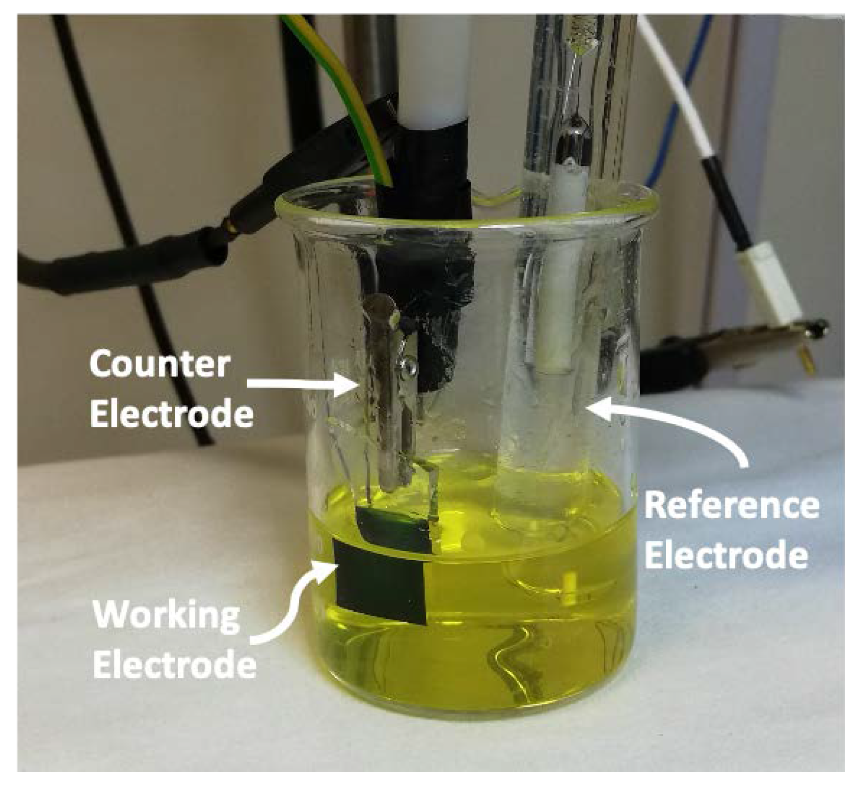
2. Materials and Methods

2.1. Chemicals

Samples were synthesized by using an electrodeposition technique with a peroxo-tungstic-acid (PTA) solution (6.5 g of W metallic powder in a mixture of 40 mL of H2O2 (30%) and 4 mL of deionized water) [18]. As this reaction is exothermic, the PTA solution was constantly stirred for 24 h in a cold bath (between 0–10 °C). The obtained colorless solution was filtered with a 0.1 μm filter and refluxed for 6 h at 55 °C in order to remove H2O2 in excess. Then, dilution with an equal volume of anhydrous absolute ethanol was operated to prevent precipitation of peroxo complexes [10], yielding a yellow-colored PTA solution (Figure 1) with a pH of 1.24. Once cooled at room temperature, the solution was used as electrolyte during electrodeposition in a three-electrode electrochemical cell (Figure 1), with an Ag/AgCl electrode as the reference electrode, a platinum wire as the counter electrode, and an Indium-Tin-Oxide (ITO) coated glass as the working electrode. The ITO substrates were cut in 1 cm × 2 cm pieces and then washed with deionized water. An area of 1 × 1 cm2 was immersed in the PTA solution. Immersed area of each sample was measured after the process, in order to have comparable current density values. To prevent PTA degradation, the solution was stored at 4 °C between different synthesis and discarded one week after preparation.
Films were deposited under potentiostatic condition, by varying deposition time (td) and applied potential (−Vd) for different samples. Just after electrodeposition, the samples, promptly rinsed with deionized water, were dark blue, but fully bleached in 1 day at room atmosphere.

2.2. Characterization

The WO3 electrodeposition was carried out by using a Versastat 4 potentiostat (Ametek, Berwyn, PA, USA) in a three-electrode setup (Figure 1). All measurements were performed at room temperature and atmospheric pressure. The morphological analyses were carried out by a scanning electron microscope (SEM) Gemini Field Emission SEM Carl Zeiss SUPRATM 25 (FEG-SEM, Carl Zeiss Microscopy GmbH, Jena, Germany). The transmittance spectra were obtained by using a UV-VIS-NIR spectrophotometer Varian Cary 500 (Varian Inc., Palo Alto, CA, USA). Atomic Force Microscopy (AFM) studies were carried out by a Bruker-Innova microscope (Bruker Corporation, Billerica, MA, USA) operating in contact mode and employing ultra-sharpened Si tips (MSNL−10 from Bruker, with anisotropic geometry, radius of curvature ∼2 nm, tip height ∼2.5 μm, front angle ∼15°, back angle ∼25°, side angle 22.5°). The Si tips were substituted as soon as a resolution loose was observed during the AFM images acquisition. Each AFM image was acquired using a scan rate of 0.3 Hz and acquiring 512 × 512 lines. The acquired AFM images were analyzed using the SPMLABANALYSES V7.00 software. The WO3 films were also analyzed by X-ray diffraction using a Bruker DiscoverTM diffractometer (Bruker Corporation, Billerica, MA, USA) equipped with thin film attachments and a K α Cu source. For the determination of W and O content, Rutherford backscattering spectrometry (RBS, 2.0 MeV He+ beam at normal incidence) with a 165° backscattering angle was employed, by using a 3.5 MV HVEE Singletron accelerator (High Voltage Engineering Europa, The Netherlands). RBS spectra were analyzed using XRump software (Thompson M., Windows (95-Win7)-Genplot and RUMP, Available online, http://www.genplot.com/download.htm).

3. Results and Discussion

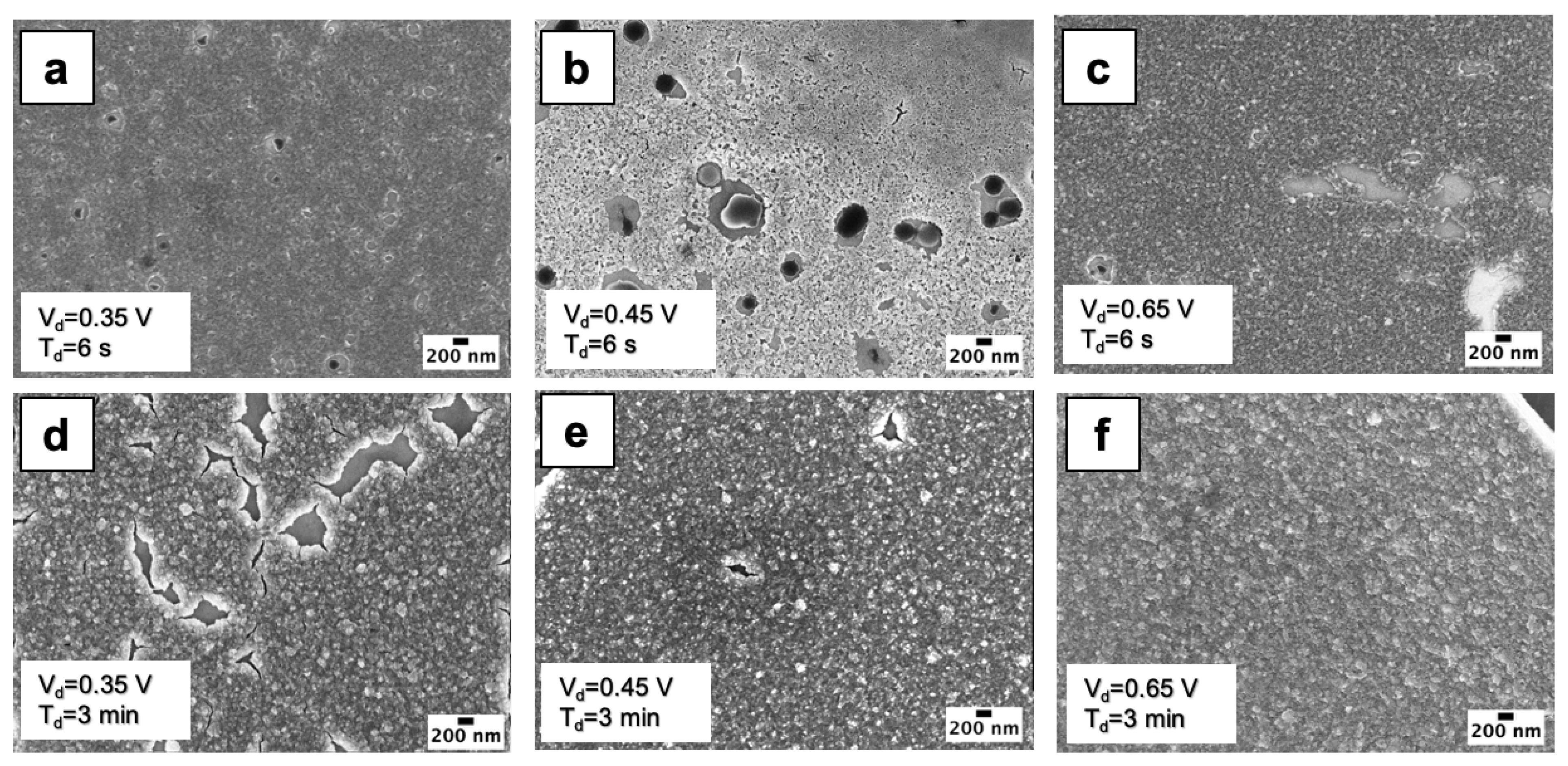
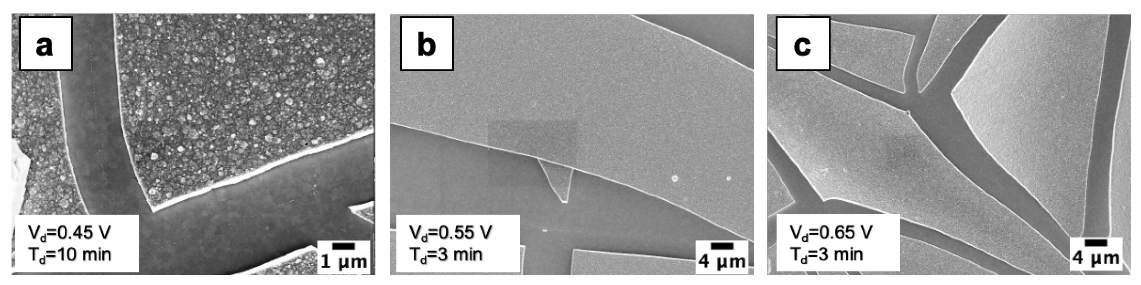
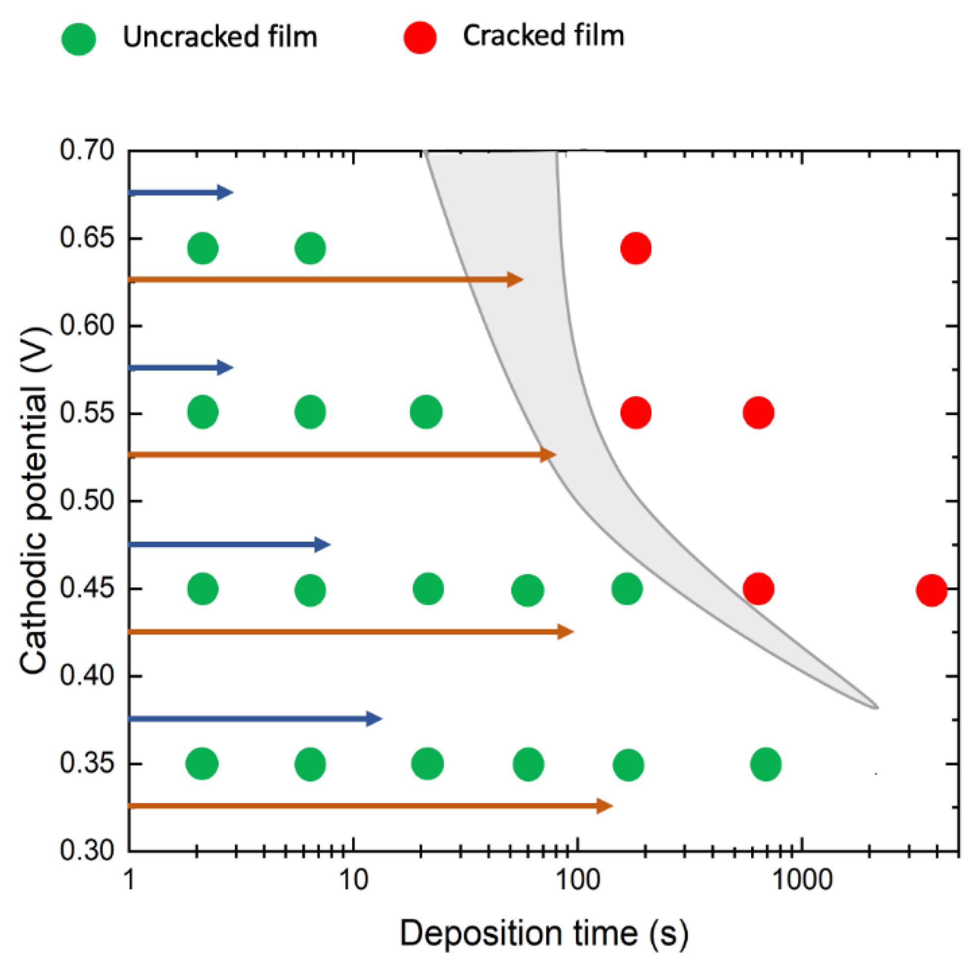
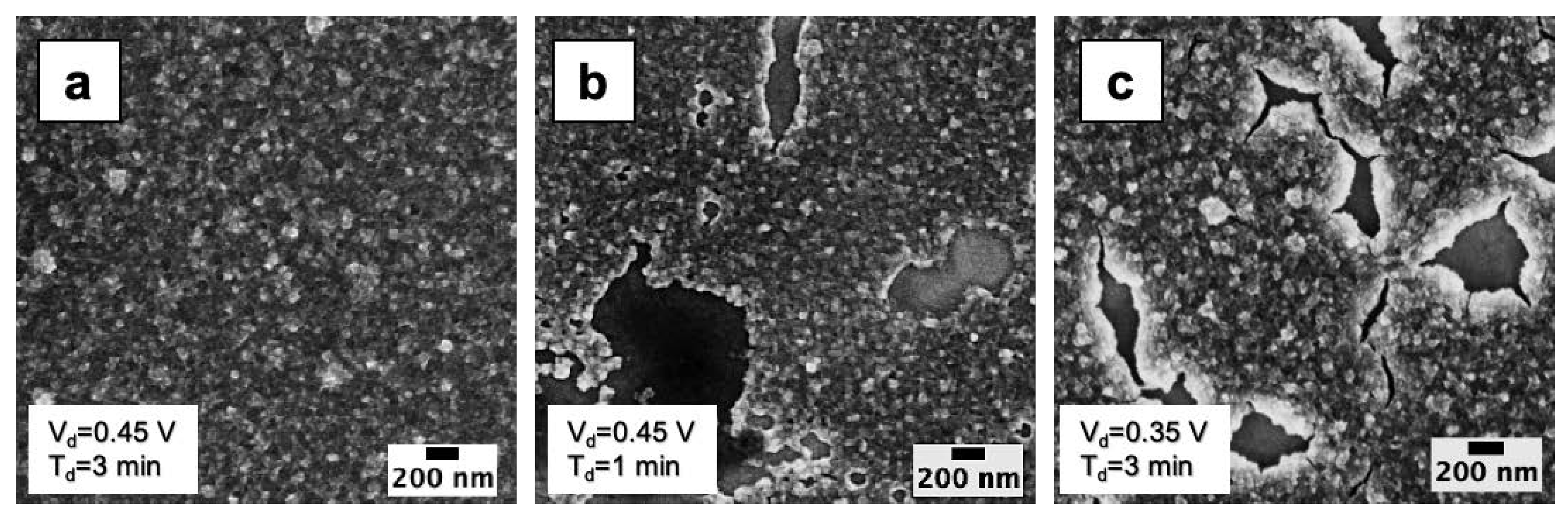
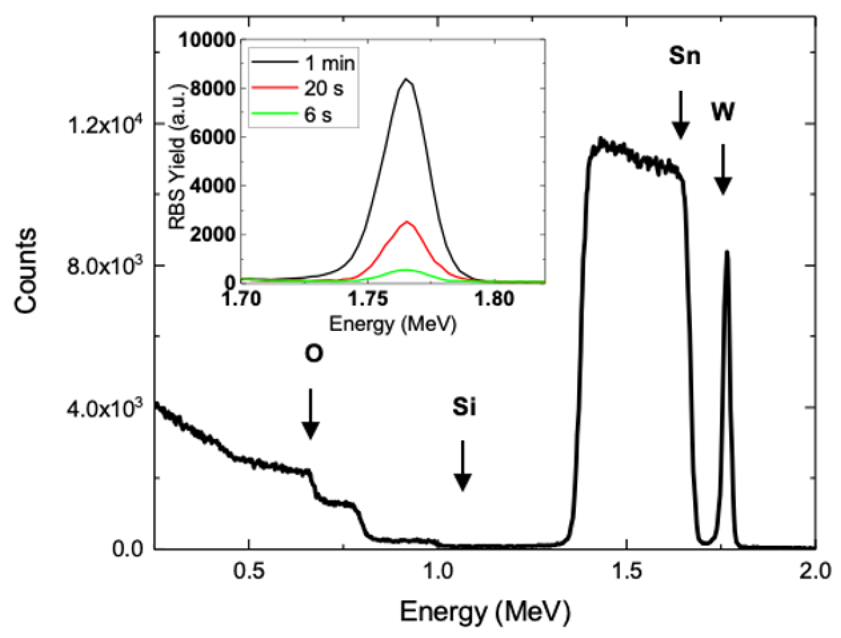
3.1. Morphological Analyses

Figure 2 shows high magnification SEM images of electrodeposited films, obtained by using different electrodeposition parameters: Vd = 0.35 V and td = 6 s (a), Vd = 0.45 V and td = 6 s (b), Vd = 0.65 V and td = 6 s (c), Vd = 0.35 V and td = 3 min (d), Vd = 0.45 V and td = 3 min (e), Vd = 0.65 V and td = 3 min (f). By observing the high magnification SEM images (Figure 2a–f) a specific common pattern can be seen, revealing that WO3 film is made of nanograins with an average lateral size of 50 nm, regardless of Vd and td. Figure S1 shows the AFM image of the sample deposited at Vd = 0.45 V for 6 s and the relative AFM line profile. The obtained size distribution confirms that the height of these nanograins is around 50 nm. Joining the AFM and SEM data we can assume that WO3 film is composed of 50 nm sized nanograins.
Figure 3a–c show SEM images of samples with broken WO3 films, with clear µm sized islands. The electrodeposition parameters used for these samples are the following: (a) Vd = 0.45 V and td = 10 min, (b) Vd = 0.55 V and td = 3 min and (c) Vd = 0.65 V and td = 3 min. The film breaking is probably caused by high mechanical stress, due to lattice mismatch, for thick WO3 film [14,26]. Thus, while for low Vd and td the films are continuous (e.g., Vd = 0.45 V for td < 10 min or Vd = 0.65 V for td < 3 min), increasing Vd and/or td leads to cracked films, as visible at Vd = 0.45 V td = 10 min (Figure 3a) or at Vd = 0.55 V td = 3 min, as well as at Vd = 0.65 V td = 3 min (Figure 3c). The WO3 islands formed after the film cracking possess the same pattern (Figure 2f), meaning that also for longer electrodeposition times WO3 nanograins are present.
For investigating the early stage growth kinetics, an uncracked film deposition is needed, thus it was useful to correlate electrodeposition parameters (Vd and td) with occurrence of film cracking. In order to do this, all samples were analyzed by SEM and placed in a deposition map (Figure 4) as a function of Vd and td. The uncracked (cracked) films are reported with green (red) balls. It is possible to individuate a border (grey colored region) between cracked and uncracked films, allowing to choose the parameter combination leading to desired WO3 films. As expected, the higher the potential is, the shorter the time to get uncracked films. In literature, to investigate the electrodeposition of WO3 films, a cathodic potential of 0.45 V for 10 min is often used [26,27]. From Figure 4 we observe that these parameters lead to cracked film, even if this combination lies very close to the border. In Figure 3a we show that using Vd = 0.45 V and td = 10 min leads to quite large (tens of µm) islands.
Even if small differences in concentration of PTA solution and/or in lab procedures can affect the border line position in our deposition map, we preferred to stay well apart from that border in order to proceed with a quantitative investigation of growth kinetics of WO3 film. Thus, in the following, only uncracked samples will be considered.
Figure S2 shows the Tauc plot obtained from a transmittance spectrum of a sample deposited with Vd = 0.45 V for 3 min. Such a combination of parameters allows to have a WO3 film thick enough to create a homogeneous film, but uncracked (Figure 4). The linear fit (red line) to Tauc plot gives information about the band gap [28], which results in 3.37 ± 0.01 eV. No correlation between the band gap value and the electrodeposition parameters is found, since the measured optical band gap in several samples ranges between 3.35 and 3.38 eV, regardless of the electrodeposition parameters. This value suggests that the film is amorphous, according to the data reported in the literature [10]. The XRD pattern of this film is reported in Figure S3, showing only peaks related to the ITO substrate and confirming the amorphous phase of the electrodeposited WO3 films.

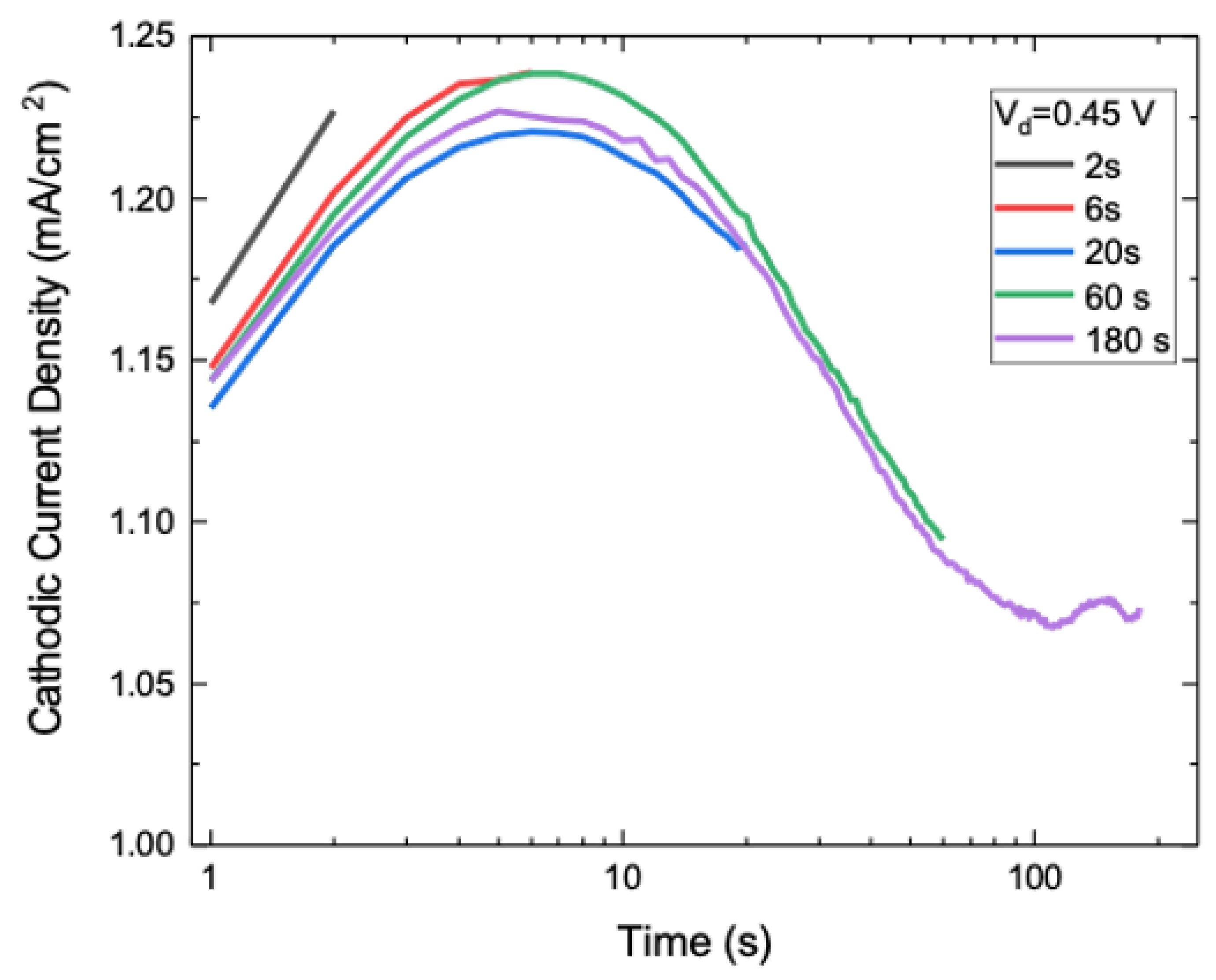
3.2. Nucleation and Growth of WO3 Films

During electrodeposition, the cathodic (negative) current is acquired as a function of time, giving insights into the kinetics of the process. As an example, in Figure 5 (lin-log scale) we report the transient of cathodic current density for five samples obtained at Vd = 0.45 V, by varying td from 2 s to 180 s. The same current transient is showed by all samples, as expected, with an increase up to a maximum (Im) at 7 s (tm) and a decrease leading to a plateau after around 100 s (ts). The measured value for current density is quite in agreement with those reported by Kwong et al. [25] at similar cathodic potential, still in our case a clear transient with a bell shape is observed.
During the first 100 s, the current shows a variation of more than 20% in its value and such a feature tells about early stage kinetics of the electrodeposition process. It should be noted that similar trends also occur for other cathodic potentials (Figure S4) with a time extent of transient lower at higher cathodic potential.
In order to account for the current transient, we considered the Sharifker–Hills model (S-H model) [29], which describes the film growth process during electrodeposition in terms of nucleation and diffusion processes. According to the S-H model, nucleation can be instantaneous or progressive. In the instantaneous case, all nucleation centers are speedily formed as electrodeposition starts and nuclei density remains constant from there on. A diffusive region starts to grow up around each nucleus leading to current increase; as soon as diffusion regions overlap each other, at t = tm, a current decrease occurs, because of the transition from convergent to linear diffusion. In the progressive nucleation, nuclei are continuously formed during growth, so that nuclei density increases linearly with time. Also in this case, a transition from convergent to linear regime is obtained at t = tm.
In Figure 6, kinetics transients for instantaneous and progressive nucleations, as described by the S-H model, are reported as normalized current, according to the following relation:
I 2 I m 2 = 1.9542 t / t m { 1 exp [ 1.2564 ( t / t m ) ] } 2
for instantaneous nucleation and
I 2 I m 2 = 1.2254 t / t m { 1 exp [ 2.3367 ( t / t m ) 2 ] } 2
for progressive nucleation [29]. It is evident that for progressive nucleation, a steeper current increase is observed in comparison to the instantaneous case, allowing to discriminate nucleation type. In the same figure we reported the experimental current transient of our sample, as an example, deposited with a cathodic potential of 0.35 V for 3 min. Our experimental transient curve shows a trend compatible with the instantaneous nucleation process. For t > tm, the experimental curve results slightly higher than the theoretical one, probably because of a more efficient diffusion process. Similar comparison was done for all experimental current transients, confirming that WO3 electrodeposition is characterized by an instantaneous nucleation process, probably ascribed to the ITO substrate in which the surface could drive a fast formation of WO3 nuclei. The instantaneous nucleation could also be confirmed by the evidence that the WO3 film is composed of 50 nm sized grains (Figure 2a–f), regardless of the cathodic potential or growth time.
In order to study the electrodeposition kinetics, it is useful to observe high resolution SEM images (Figure 7) referring to early stage growth. At cathodic potential of 0.45 V, tm and ts are 7 s and 100 s, respectively, thus we found, as expected, a full coverage of substrate only after 100 s (Figure 7a), while at 60 s the electrodeposited WO3 (Figure 7b) presents many holes (200 nm sized) waiting to be filled by prolonging the growth. By reducing the cathodic potential to 0.35 V, a depositon of 3 min (Figure 7c) gives a similar result to the 60 s-0.45 V sample, with many holes surrounded by the growing WO3. Thus, we can assume that the electrodeposition transient proceeds with the growth of isolated grains up to tm, then merging of grains occurs roughly up to ts, and an almost continuous film is achieved after ts. Such considerations are useful to drive the deposition of a nanostructured versus continuous WO3 film, as for times between tm and ts, the uncomplete substrate coverage, leading to the observed holes, could increase the surface over volume ratio of W oxide.

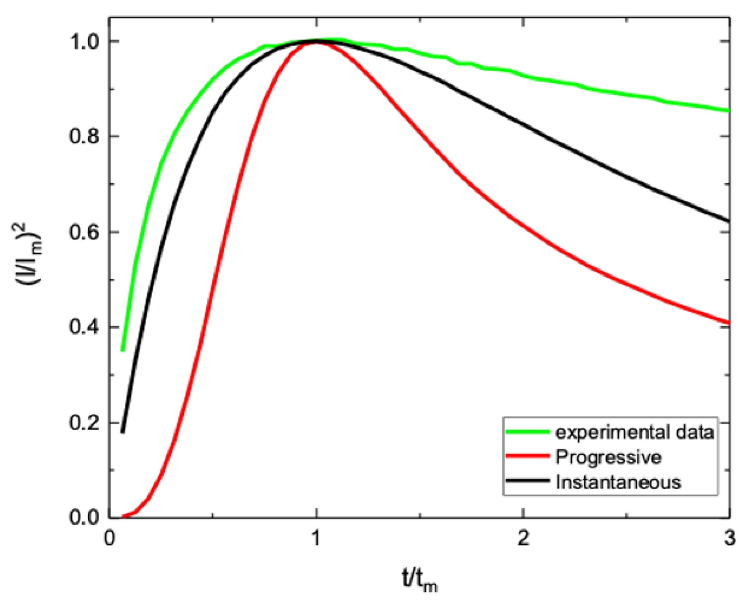
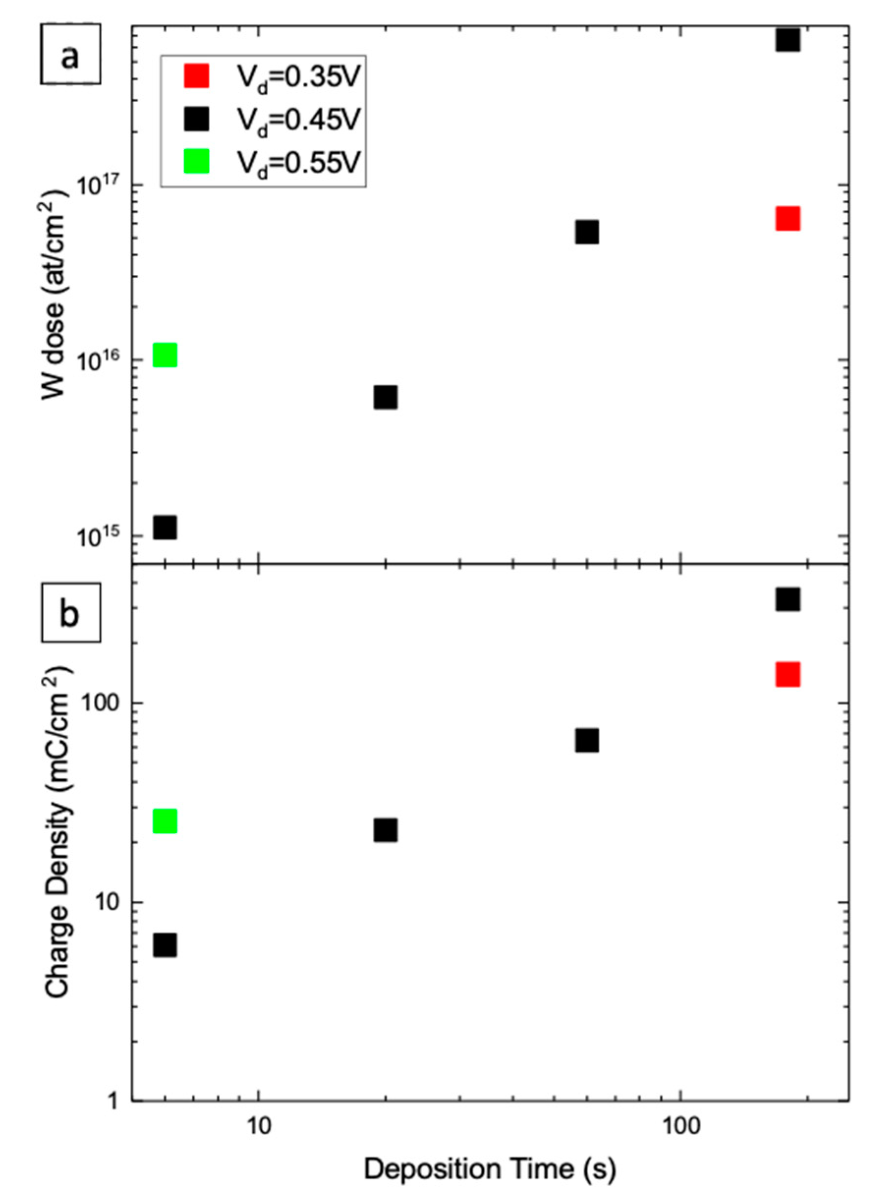
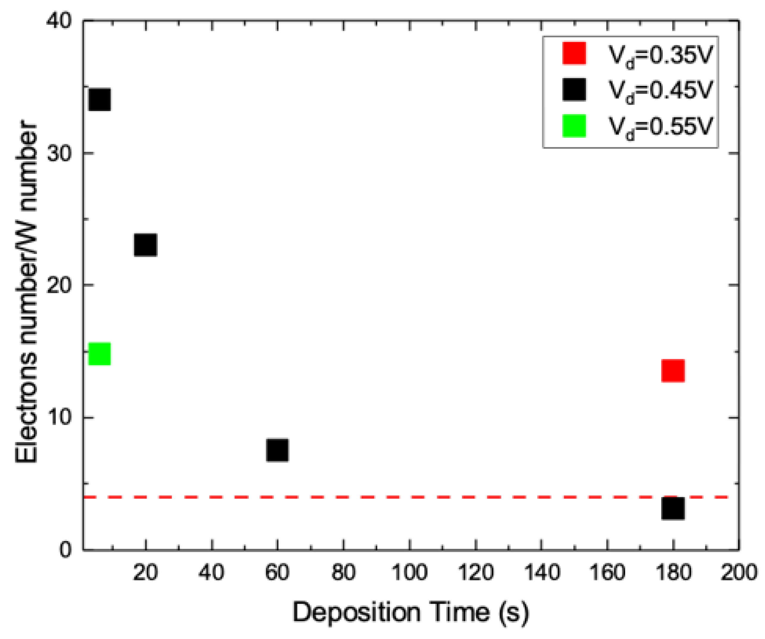
3.3. Model for WO3 Electrodeposition

Figure 8 shows the RBS spectra of samples deposited at 0.45 V for 60 s. The arrows indicate the energy of He ions backscattered by W (1.836 MeV), Sn (1.752 MeV), Si (1.138 MeV) or O (731.8 keV) atoms on the surface of analyzed films. The signals for W and O are present as expected, while Sn (present in the ITO) and Si (glass below ITO) ones appear at lower energy since they are buried below WO3 and ITO films, respectively. The inset reports only the W signal at increasing deposition times. The area below the W peak quantifies the W dose on the analyzed sample. The result of such exercise is reported in Figure 9a for different deposition parameters. The O content of the WO3 film is more challenging because of the overlapping of the RBS signal related to underlying layers (ITO and glass). To overcome this, RBS spectra in the glancing configuration were acquired to enhance backscattering from the surface (Figure S5). A W:O = 1:3 stoichiometry was obtained by comparing the O and W dose in selected samples.
Figure 9a (log-log scale) reports the dose of W in electrodeposited films as a function of td. An increase with time of W dose is visible for 0.45 V. At lower and higher cathodic potential, a corresponding lower and higher W dose is found, as expected. As far as the W deposition rate is concerned, at 6 s an average value of 1.7 × 10¹⁴ at./cm2 s is obtained, while at 180 s, the average rate increases to 4 × 10¹⁵ at./cm2 s. Figure 9b shows the time variation of electrical charge exchanged at working electrode per unit area of WO3 film (obtained as time integral of current density). These last data follow the same trend observed in Figure 9a and roughly agree with W dose, suggesting that with increasing current an increasing deposition rate occurs. In order to correlate these data with the growth kinetics, a model for the WO3 electrodeposition is needed.
According to Meulenkamp, electrodeposition of WO3 from a PTA solution proceeds via a reduction process, starting with PTA dissociation [30]
2 W + 10 H 2 O 2 W 2 O 11 2 + 2 H + + 9 H 2 O
and followed by reduction of the peroxotungstate ion W2O112− towards WO3 formation [30]
W 2 O 11 2 + ( 2 + 2 x ) H + + 2 xe 2 WO 3 + 2 + 2 x 2 H 2 O + 8 2 x 4 O 2
In the last reaction, x is the number of electrons exchanged to deposit a single WO3 unit, thus relating the current at the working electrode to the deposition rate. According to the above chemical reaction, x = 0 or 4 leads to high or null O2 production. A high (low) value of x is related to a low (high) effectiveness of current versus deposition rate, since a large (small) current exchanged at the working electrode is required to proceed with WO3 deposition. Meulenkamp experimentally showed that x ranges between 1 and 3.5 [30].
Figure 10 reports the x value measured per each sample. This value is the ratio between W dose (Figure 9a) and charge exchanged at the working electrode (Figure 9b). For a cathodic potential of 0.45 V, a decreasing trend for x is clearly visible with time, starting from x = 34 at the beginning, and reaching x = 3.12 only at 180 s, well after ts. This reveals that for the whole transient the effectiveness of current versus deposition rate is very low. In fact, at early stage the W deposition rate is quite low in comparison to longer times, but it requires a current higher than at longer times. It is worth noting that x reaches a value which is in accordance with the reaction (2) as soon as the transient ends up, i.e., at ts. After the current transient, the growth of WO3 film proceeds with an effective use of exchanged charges at the working electrode. In comparison to 0.45 V, higher or lower cathodic potentials leads to lower or higher x values for the same deposition time. This evidence confirms that the effectiveness of current is potential dependent as the current transient is.
After the transient, the WO3 deposition seems to be compatible with the following reaction:
W 2 O 11 2 + 10 H + + 8 e 2 W O 3 + 5 H 2 O
for which no O2 production is needed. For longer times, the x value saturates and a constant chemical reaction like the above one can describe the WO3 electrodeposition. At the early stage, some auxiliary process must be invoked to account for the larger current observed. Actually, during the transient an evident color change of samples is observed, which can be caused by an H intercalation [1,2], made even more effective by the holes present in the WO3 layer (Figure 7). The H intercalation is a reduction process, which can explain the quite larger current and the very high x value observed during the transient.

4. Conclusions

The electrodeposition of WO3 film from a PTA solution was investigated at different cathodic potentials (0.35–0.65 V) and deposition times (2–1800 s). At long times and/or high cathodic potential, a broken WO3 film is obtained. Several combinations of electrodeposition parameters (deposition map) have been used to investigate the film synthesis and its morphology (continuous or broken films). The growth kinetics before breaking were deeply investigated. The electrodeposition of a WO3 film proceeds with an initial transient stage, with partial coverage of the substrate and a time-dependent current, followed by a steady state stage leading to continuous film and constant current. The WO3 electrodeposition on ITO substrates shows an instantaneous nucleation and is diffusion-controlled, producing nanostructured films (50 nm sized grains) with 1:3 W:O stoichiometry. A quantitative analysis compared the current at the working electrode to the W deposition rate, validating a chemical reaction underlying the microscopic mechanism for WO3 deposition at longer times. At the early stages of deposition, a larger current is observed despite a reduced W deposition rate, and a possible H intercalation process is discussed. The reported modeling of the electrodeposition process can be suitable for a controlled synthesis of WO3 nanostructures.

Supplementary Materials

The following are available online at https://www.mdpi.com/2079-4991/10/8/1493/s1, Figure S1: (a) AFM image of the sample deposited by applying Vd = 0.45 V for 6 s. The blue line identifies the region in which the line spectrum showed in (b) is obtained, Figure S2: Tauc plot of sample deposited at Vd = 0.45 V for 3 min. The red line is the linear fit, Figure S3: XRD pattern of the sample deposited by applying Vd = 0.45 V for 3 min. The peaks are related to the ITO presence in the substrate, Figure S4: Current transients recorded during the samples electrodeposition by applying different Vd for 3 min. The dotted lines allow to individuate the different ts for the different Vd values, Figure S5: RBS spectrum, of the sample deposited by using Vd = 0.45 V for 1 min, acquired in glancing configuration. The red line is the line of the background, which was subtracted in order to individuate the peak related to the O content (green line).

Author Contributions

Conceptualization, S.M. and E.B.; investigation, G.M., F.R., S.M. and E.B.; methodology, G.M., S.M. and E.B.; supervision, S.M. and E.B.; writing—original draft, G.M.; writing—review and editing, G.M., F.R., S.M. and E.B. All authors have read and agreed to the published version of the manuscript.

Funding

This work was supported by “programma ricerca di Ateneo UNICT 2020-22 linea 2”, by PRIN 2017 “CLEAN-Valorizing Sustainable Plastics through a CLEver use of NANoparticles” 20174FSRZS_003 and by “PON MIUR ADAS +” (ARS01_00459).

Acknowledgments

The authors wish to thank A. Alberti (CNR-IMM Catania, Italy) for useful discussions and experimental XRD contribution and G. Pantè, C. Percolla and S. Tatì (CNR-IMM Catania, Italy) for technical support.

Conflicts of Interest

The authors declare no conflict of interest.

References

  1. Deb, S.K. Opportunities and challenges in science and technology of WO3 for electrochromic and related applications. Sol. Energy Mater. Sol. Cells 2008, 92, 245–258. [Google Scholar] [CrossRef]
  2. Granqvist, C.G. Electrochromic tungsten oxide films: review of progress 1993–1998. Sol. Energy Mater. Sol. Cells 2000, 60, 201–262. [Google Scholar] [CrossRef]
  3. Thummavichai, K.; Xia, Y.; Zhu, Y. Recent progress in chromogenic research of tungsten oxides towards energy-related applications. Prog. Mater. Sci. 2017, 88, 281–324. [Google Scholar] [CrossRef]
  4. Ahsan, M.; Tesfamichael, T.; Ionescu, M.; Bell, J.; Motta, N. Low temperature CO sensitive nanostructured WO3 thin films doped with Fe. Sens. Actuators B Chem. 2012, 162, 14–21. [Google Scholar] [CrossRef] [Green Version]
  5. Kida, T.; Nishiyama, A.; Hua, Z.; Suematsu, K.; Yuasa, M.; Shimanoe, K. WO3 nanolamella gas sensor: porosity control using SnO2 nanoparticles for enhanced NO2 sensing. Langmuir 2014, 30, 2571–2579. [Google Scholar] [CrossRef]
  6. Ponzoni, A.; Comini, E.; Ferroni, M.; Sberveglieri, G. Nanostructured WO3 deposited by modified thermal evaporation for gas-sensing applications. Thin Solid Films 2005, 490, 81–85. [Google Scholar] [CrossRef]
  7. Grace, P.S.; Devadasan, J.J.; Jeyadheepan, K.; Thangam, G.J. Room temperature NH3-sensing properties of WO3 thin films synthesized by microprocessor controlled spray pyrolysis. IOSR J. Appl. Phys. 2017, 3, 52–56. [Google Scholar] [CrossRef]
  8. Shi, J.; Cheng, Z.; Gao, L.; Zhang, Y.; Xu, J.; Zhao, H. Facile synthesis of reduced graphene oxide/hexagonal WO3 nanosheets composites with enhanced H2S sensing properties. Sens. Actuators B Chem. 2016, 230, 736–745. [Google Scholar] [CrossRef]
  9. Kalantar-zadeh, K.; Fry, B. Nanotechnology-Enabled Sensors; Springer Science & Business Media: Medford, MA, USA, 2007. [Google Scholar]
  10. Zheng, H.; Ou, J.Z.; Strano, M.S.; Kaner, R.B.; Mitchell, A.; Kalantar-zadeh, K. Nanostructured tungsten oxide-properties, synthesis, and applications. Adv. Funct. Mater. 2011, 21, 2175–2196. [Google Scholar] [CrossRef]
  11. Lee, S.H.; Deshpande, R.; Parilla, P.A.; Jones, K.M.; To, B.; Mahan, A.H.; Dillon, A.C. Crystalline WO3 nanoparticles for highly improved electrochromic applications. Adv. Mater. 2006, 18, 763–766. [Google Scholar] [CrossRef]
  12. Karakurt, İ.; Boneberg, J.; Leiderer, P. Electrochromic switching of WO3 nanostructures and thin films. Appl. Phys. A 2006, 83, 1–3. [Google Scholar] [CrossRef] [Green Version]
  13. Nah, Y.C.; Ghicov, A.; Kim, D.; Schmuki, P. Enhanced electrochromic properties of self-organized nanoporous WO3. Electrochem. commun. 2008, 10, 1777–1780. [Google Scholar] [CrossRef]
  14. Kim, Y.O.; Yu, S.H.; Ahn, K.S.; Lee, S.K.; Kang, S.H. Enhancing the photoresponse of electrodeposited WO3 film: Structure and thickness effect. J. Electroanal. Chem. 2005, 752, 25–32. [Google Scholar] [CrossRef]
  15. Lemire, C.; Lollman, D.B.; Al Mohammad, A.; Gillet, E.; Aguir, K. Reactive RF magnetron sputtering deposition of WO3 thin films. Sens. Actuators B Chem. 2005, 84, 43–48. [Google Scholar] [CrossRef]
  16. Hong, K.; Xie, M.; Wu, H. Tungsten oxide nanowires synthesized by a catalyst-free method at low temperature. Nanotechnology 2006, 17, 4830. [Google Scholar] [CrossRef]
  17. Djaoued, Y.; Priya, S.; Balaji, S. Low temperature synthesis of nanocrystalline WO3 films by sol-gel process. J. Non Cryst. Solids 2008, 354, 673–679. [Google Scholar] [CrossRef]
  18. Deepa, M.; Kar, M.; Agnihotry, S.A. Electrodeposited tungsten oxide films: annealing effects on structure and electrochromic performance. Thin Solid Films 2004, 468, 32–42. [Google Scholar] [CrossRef]
  19. Kalhori, H.; Ranjbar, M.; Salamati, H.; Coey, J.M.D. Flower-like nanostructures of WO3: Fabrication and characterization of their in-liquid gasochromic effect. Sens. Actuators B Chem. 2016, 225, 535–543. [Google Scholar] [CrossRef]
  20. Poongodi, S.; Kumar, P.S.; Mangalaraj, D.; Ponpandian, N.; Meena, P.; Masuda, Y.; Lee, C. Electrodeposition of WO3 nanostructured thin films for electrochromic and H2S gas sensor applications. J. Alloys Compd. 2017, 719, 71–81. [Google Scholar] [CrossRef]
  21. Deepa, M.; Srivastava, A.K.; Sood, K.N.; Agnihotry, S.A. Nanostructured mesoporous tungsten oxide films with fast kinetics for electrochromic smart windows. Nanotechnology 2006, 17, 2625. [Google Scholar] [CrossRef]
  22. More, A.J.; Patil, R.S.; Dalavi, D.S.; Mali, S.S.; Hong, C.K.; Gang, M.G.; Patil, P.S. Electrodeposition of nano-granular tungsten oxide thin films for smart window application. Mater. Lett. 2014, 134, 298–301. [Google Scholar] [CrossRef]
  23. Baeck, S.H.; Jaramillo, T.; Stucky, G.D.; McFarland, E.W. Controlled electrodeposition of nanoparticulate tungsten oxide. Nano Lett. 2002, 2, 831–834. [Google Scholar] [CrossRef]
  24. Vijayakumar, E.; Yun, Y.H.; Quy, V.H.V.; Lee, Y.H.; Kang, S.H.; Ahn, K.S.; Lee, S.W. Development of tungsten trioxide using pulse and continuous electrodeposition and its properties in electrochromic devices. J. Electrochem. Soc. 2019, 166, D86. [Google Scholar] [CrossRef]
  25. Kwong, W.L.; Savvides, N.; Sorrel, C.C. Electrodeposited nanostructured WO3 thin films for photoelectrochemical applications. Electrochim. Acta 2012, 75, 371–380. [Google Scholar] [CrossRef]
  26. Leftheriotis, G.; Yianoulis, P. Development of electrodeposited WO3 films with modified surface morphology and improved electrochromic properties. Solid State Ionics 2008, 179, 2192–2197. [Google Scholar] [CrossRef]
  27. Srivastava, A.K.; Deepa, M.; Singh, S.; Kishore, R.; Agnihotry, S.A. Microstructural and electrochromic characteristics of electrodeposited and annealed WO3 films. Solid State Ionics 2005, 176, 1161–1168. [Google Scholar] [CrossRef]
  28. Raciti, R.; Bahariqushchi, R.; Summonte, C.; Aydinli, A.; Terrasi, A.; Mirabella, S. Optical bandgap of semiconductor nanostructures: methods for experimental data analysis. J. Appl. Phys. 2017, 121, 234304. [Google Scholar] [CrossRef]
  29. Scharifker, B.; Hills, G. Theoretical and experimental studies of multiple nucleation. Electrochim. Acta 1983, 28, 879–889. [Google Scholar] [CrossRef]
  30. Meulenkamp, E.A. Mechanism of WO3 Electrodeposition from Peroxy-Tungstate Solution. J. Electrochem. Soc. 1997, 144, 1664. [Google Scholar] [CrossRef]
Figure 1. Experimental setup for the electrodeposition of WO3 films. It is possible to distinguish the working electrode, the counter electrode and the reference electrode. They are immersed into the peroxo-tungstic acid (PTA) solution.
Nanomaterials 10 01493 g001
Figure 2. SEM images of electrodeposited WO3 by using: (a) Vd = 0.35 V and td = 6 s; (b) Vd = 0.45 V and td = 6 s; (c) Vd = 0.65 V and td = 6 s; (d) Vd = 0.35 V and td = 3 min; (e) Vd = 0.45 V and td = 3 min; (f) Vd = 0.65 V and td = 3 min. It is possible to observe the characteristic pattern with nanograins (50 nm lateral size) regardless of Vd and td.
Nanomaterials 10 01493 g002
Figure 3. SEM images of electrodeposited WO3 by using: (a) Vd = 0.45 V and td = 10 min; (b) Vd = 0.55 V and td = 3 min; (c) Vd = 0.65 V and td = 3 min.
Nanomaterials 10 01493 g003
Figure 4. Deposition map: each electrodeposited sample is reported here as a function of Vd and td. The WO3 films are reported as green or red dots if they result uncracked or cracked, respectively. Per each deposition at fixed Vd, two arrows indicate the time extent to get the maximum current (tm, blue arrow) or the saturation current (ts, orange arrow) measured during the electrodeposition (see Figure 5).
Nanomaterials 10 01493 g004
Figure 5. Current transients recorded during the samples electrodeposition at Vd = 0.45 V.
Nanomaterials 10 01493 g005
Figure 6. Comparison between the experimental data (green curve) and the theoretical data of the Sharifker–Hills model for instantaneous and progressive nucleation (black and red curve, respectively). The experimental curve is related to electrodeposition of WO3 by using Vd = 0.35 V and td = 3 min.
Nanomaterials 10 01493 g006
Figure 7. High resolution SEM images of the samples deposited by applying (a) 0.45 V for 3 min, (b) 0.45 V for 1 min and (c) 0.35 V for 3 min.
Nanomaterials 10 01493 g007
Figure 8. Rutherford backscattering spectrometry (RBS) spectra of electrodeposited WO3. The normal configuration is used for the determination of W dose from the integration of the peak related to the W presence for the sample deposited by using Vd = 0.45 V for 1 min; Inset: W peak of samples deposited by using Vd = 0.45 V for 6 s, 20 s and 1 min.
Nanomaterials 10 01493 g008
Figure 9. (a) W dose obtained from RBS spectra as a function of td for different Vd values; (b) charge density obtained from the integration of the current transient as a function of td for different Vd values.
Nanomaterials 10 01493 g009
Figure 10. Exchanged electrons during the deposition of a single W atom for the samples deposited at different Vd for different td.
Nanomaterials 10 01493 g010

