Conductive Atomic Force Microscopy of Semiconducting Transition Metal Dichalcogenides and Heterostructures


Abstract
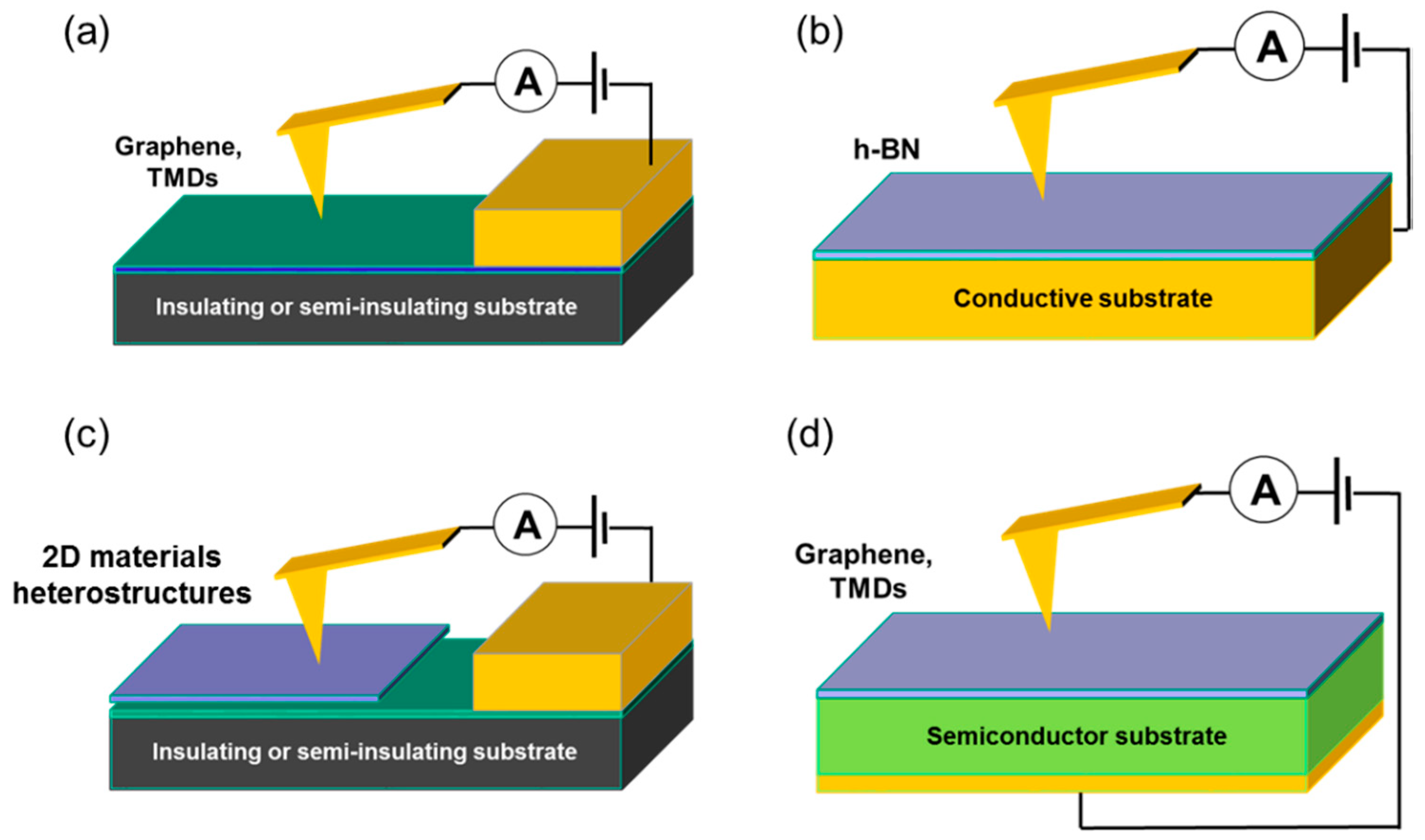
:1. Introduction
2. Schottky Barrier Height Mapping at Metal/TMDs Junction
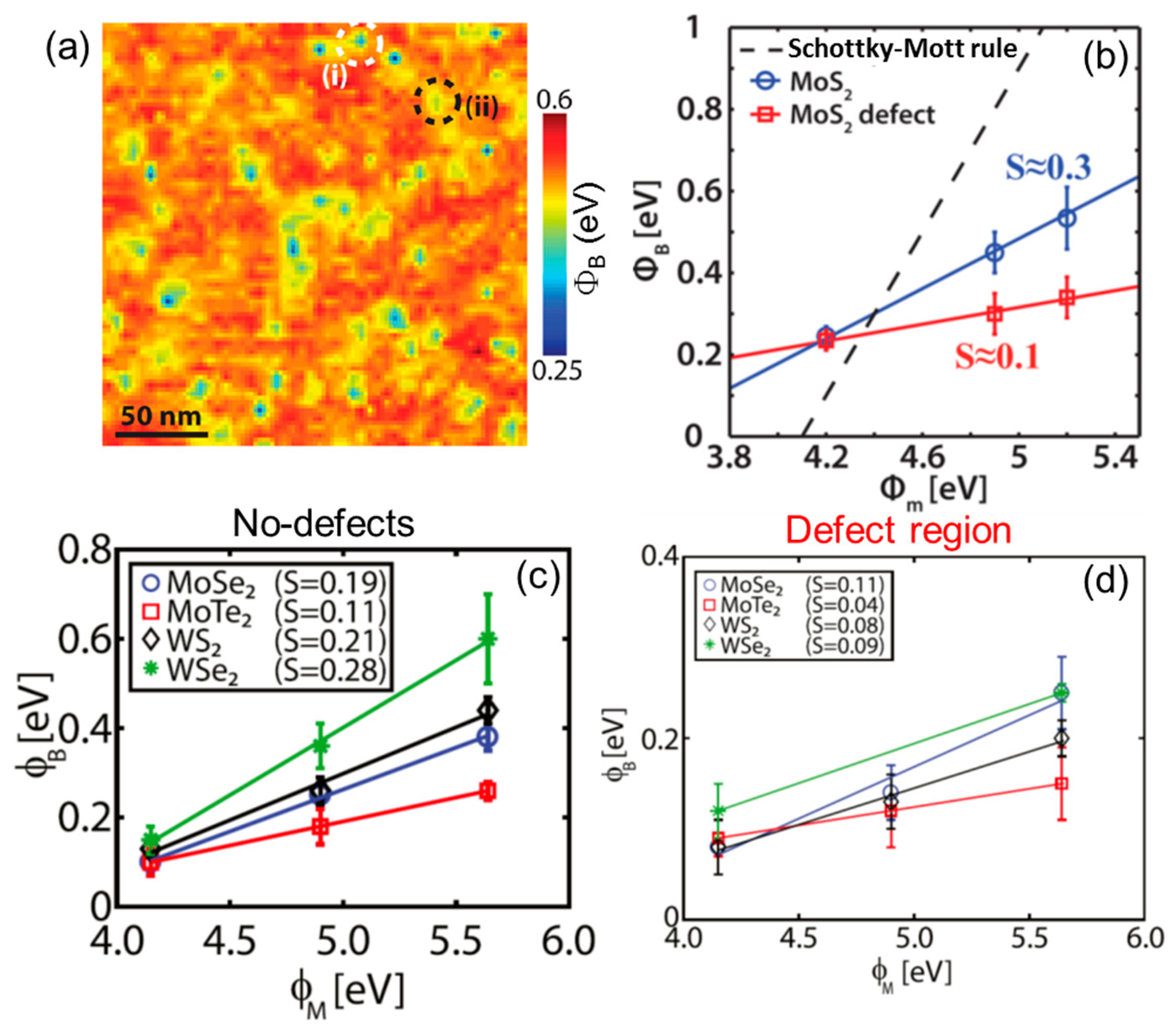
2.1. C-AFM Investigations of Fermi Level Pinning in TMDs
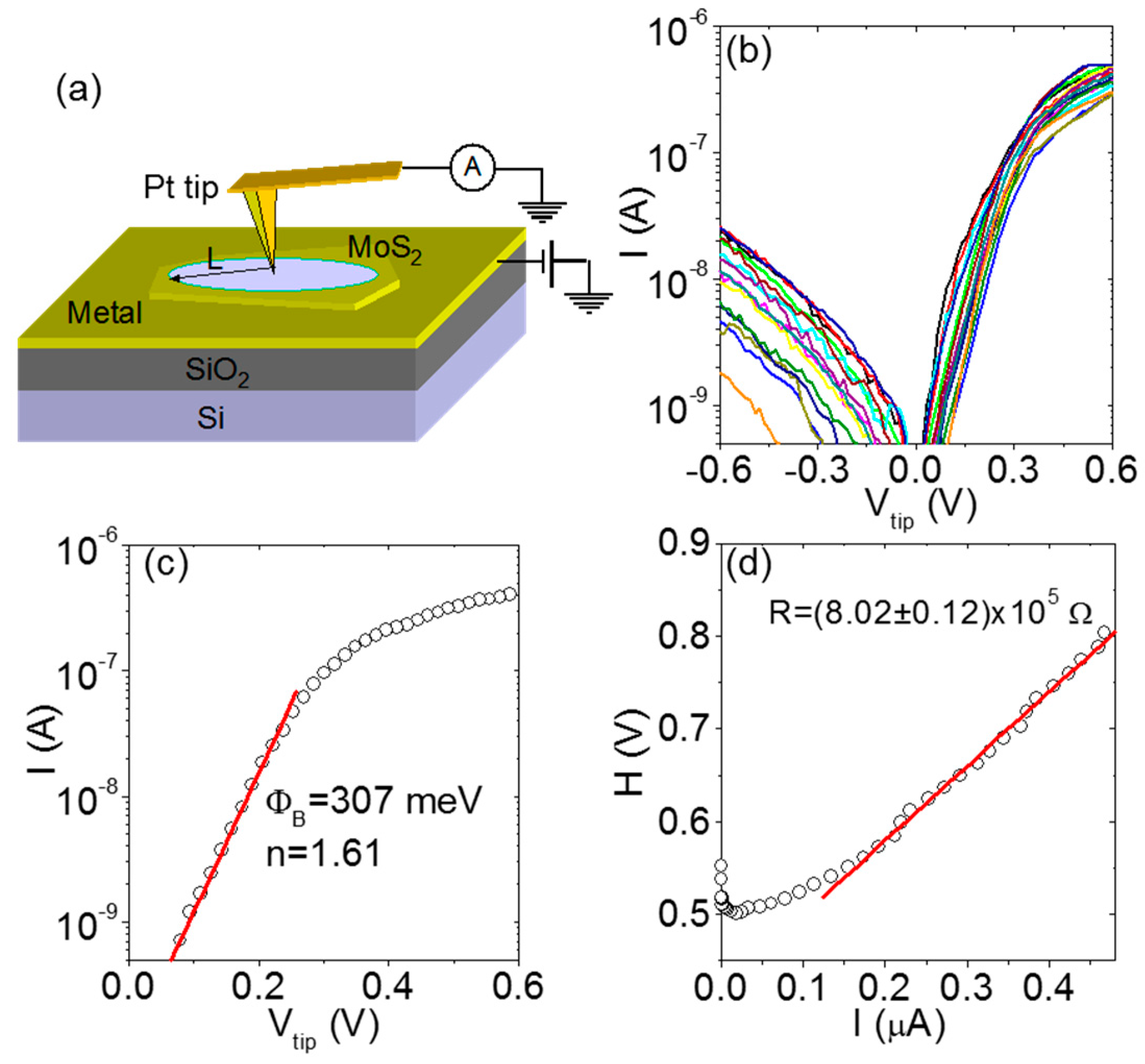
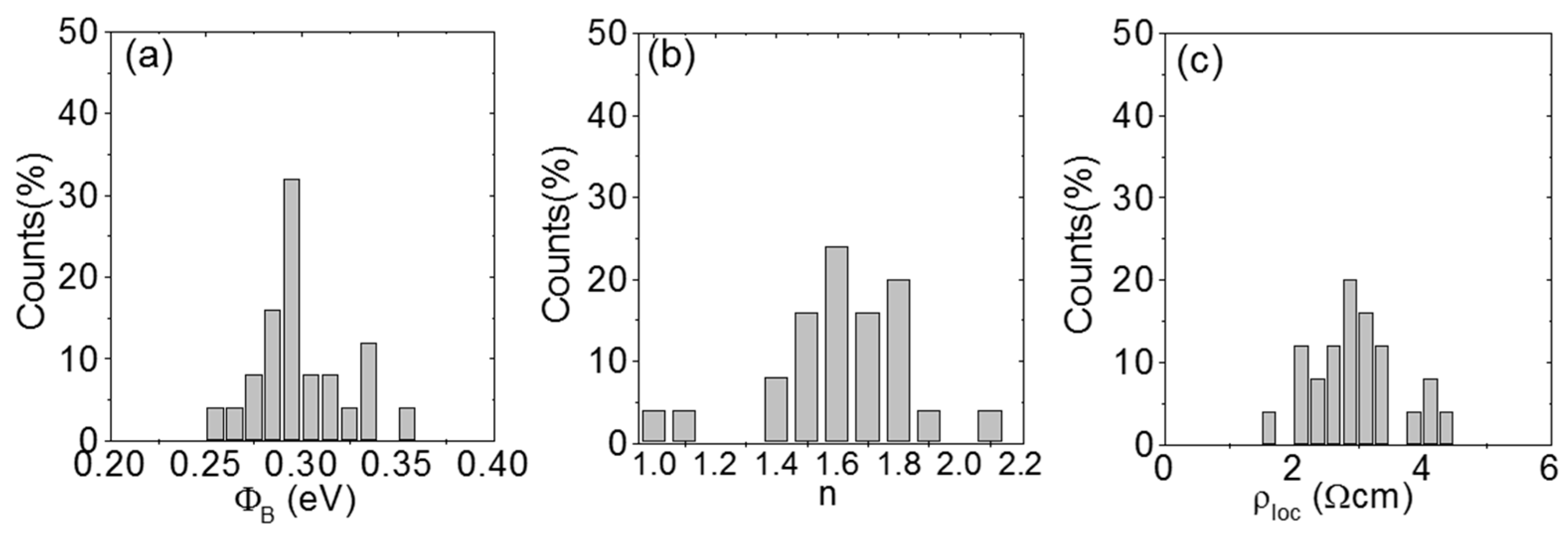
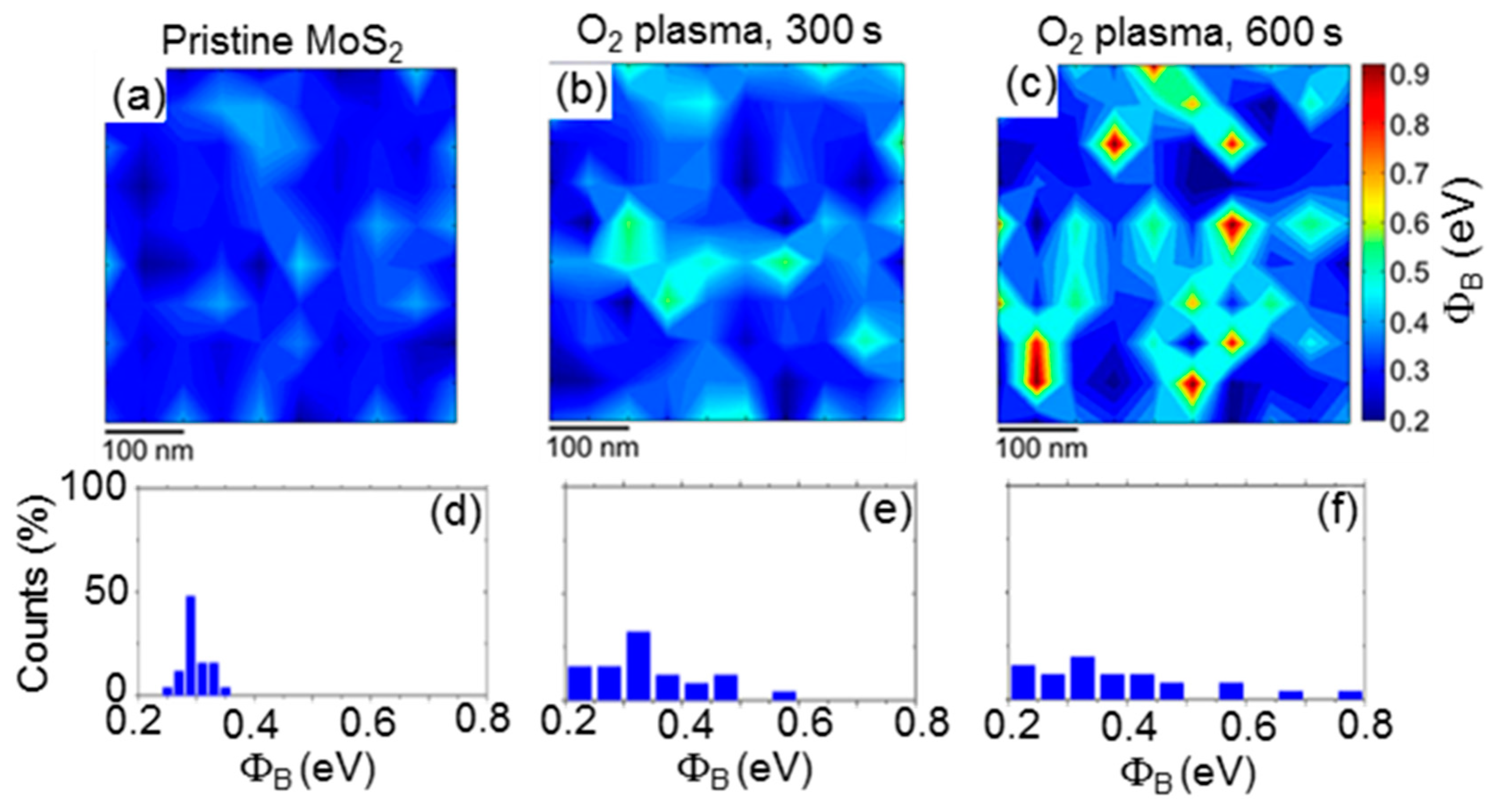
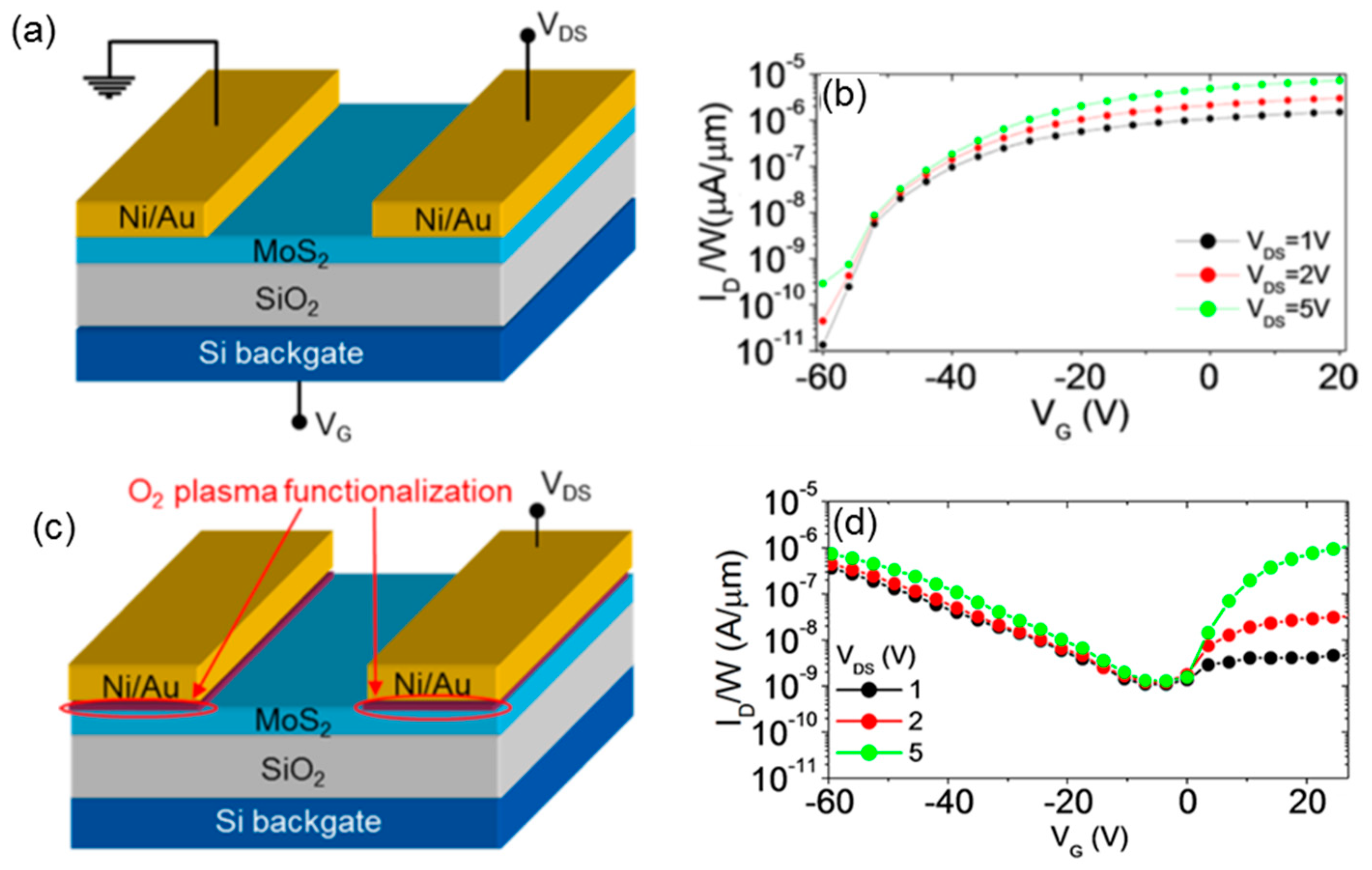
2.2. Nanoscale Mapping of MoS2 Schottky Barrier Tuned by Oxygen Plasma Treatments
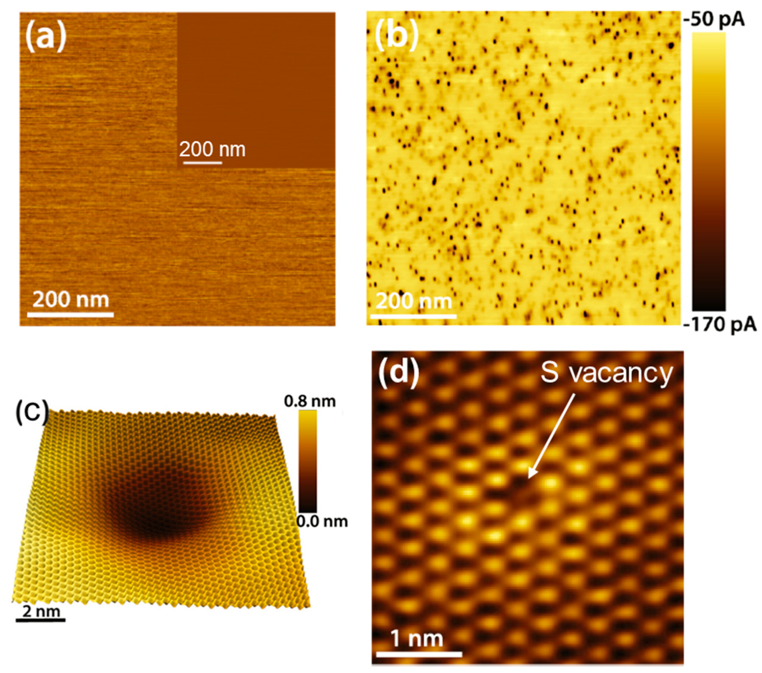
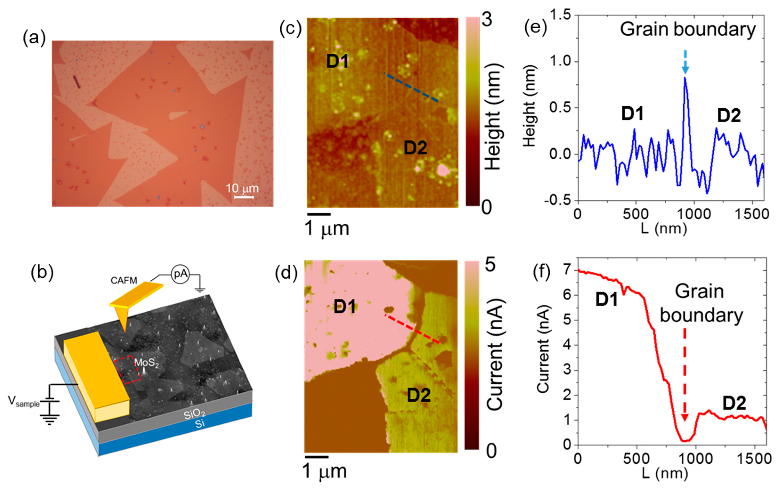
3. Local Resistance Mapping at Grain Boundaries in CVD Grown MoS2
4. Local Transport Properties in TMD Lateral and Vertical Heterojunctions
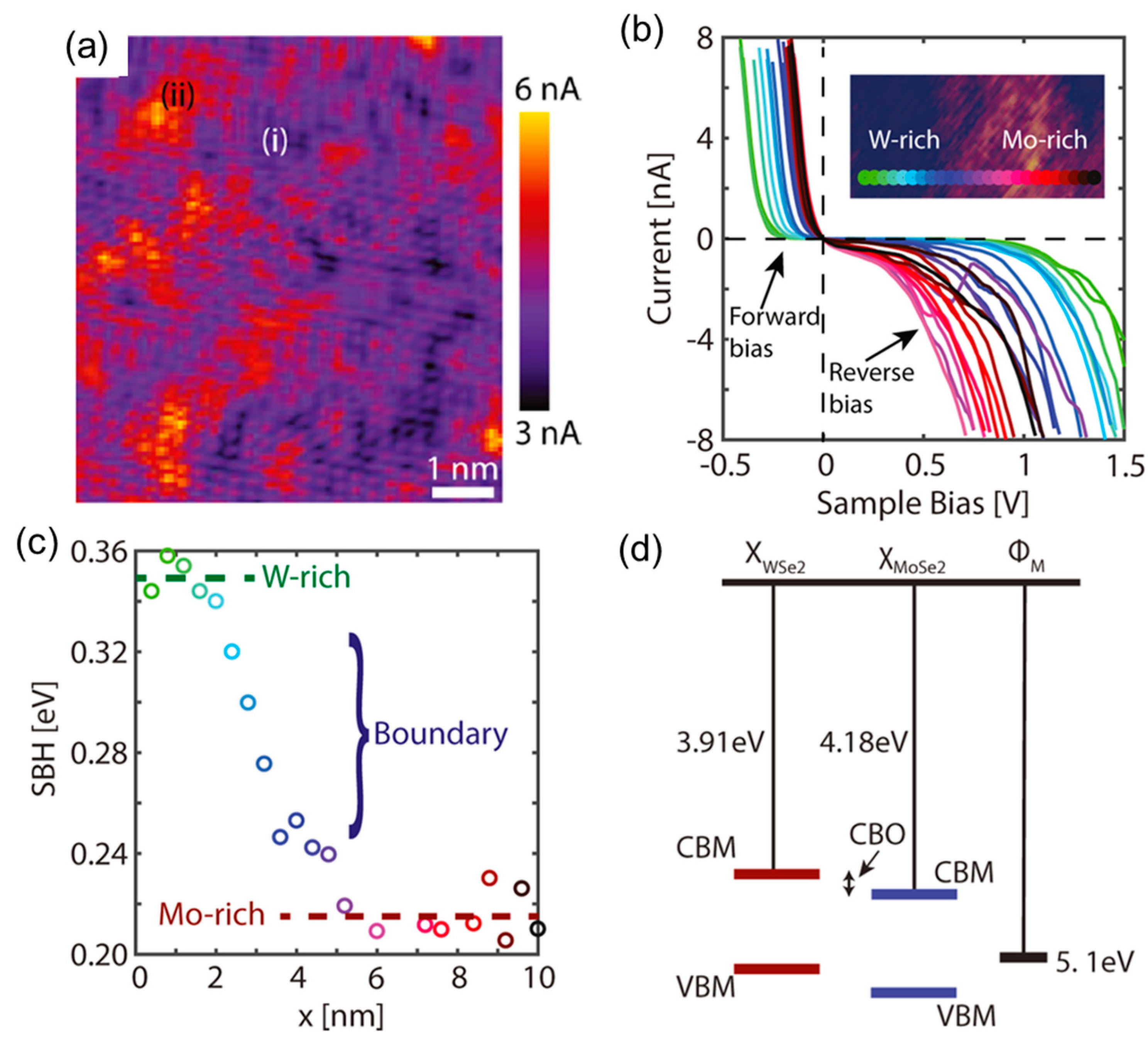
4.1. Lateral Heterojunctions of TMDs
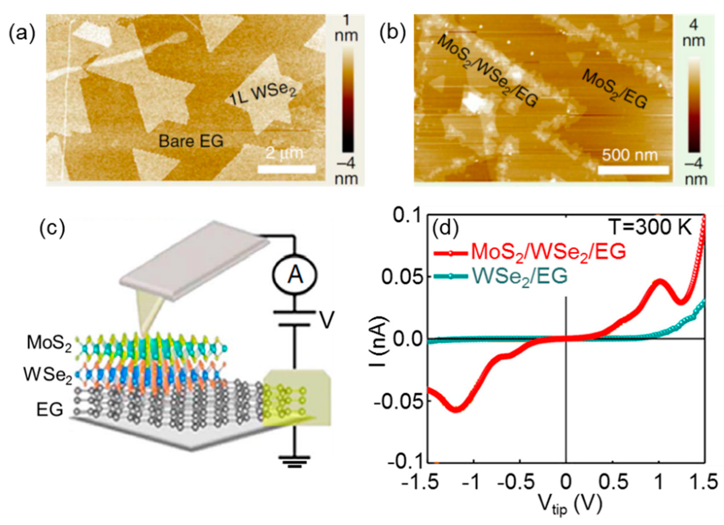
4.2. Vertical Heterostructures of TMDs
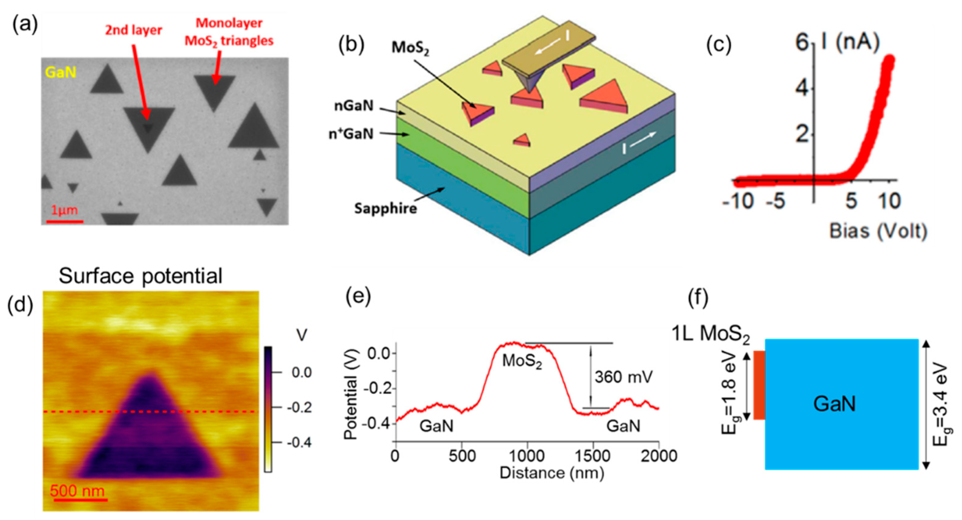
4.3. Vertical Heterostructures of TMDs with Bulk Semiconductors
5. Conclusions and Perspectives
Author Contributions
Funding
Acknowledgments
Conflicts of Interest
References
- Wang, Q.H.; Kalantar-Zadeh, K.; Kis, A.; Coleman, J.N.; Strano, M.S. Electronics and Optoelectronics of Two-Dimensional Transition Metal Dichalcogenides. Nat. Nanotechnol. 2012, 7, 699. [Google Scholar] [CrossRef]
- Duan, X.; Wang, C.; Pan, A.; Yu, R.; Duan, X. Two-Dimensional Transition Metal Dichalcogenides as Atomically Thin Semiconductors: Opportunities and Challenges. Chem. Soc. Rev. 2015, 44, 8859–8876. [Google Scholar] [CrossRef]
- Splendiani, A.; Sun, L.; Zhang, Y.; Li, T.; Kim, J.; Chim, C.-Y.; Galli, G.; Wang, F. Emerging Photoluminescence in Monolayer MoS2. Nano Lett. 2010, 10, 1271–1275. [Google Scholar] [CrossRef] [PubMed]
- Radisavljevic, B.; Radenovic, A.; Brivio, J.; Giacometti, V.; Kis, A. Single-Layer MoS2 Transistors. Nat. Nanotechnol. 2011, 6, 147–150. [Google Scholar] [CrossRef]
- Kim, S.; Konar, A.; Hwang, W.S.; Lee, J.H.; Lee, J.; Yang, J.; Jung, C.; Kim, H.; Yoo, J.B.; Choi, J.Y.; et al. High-Mobility and Low-Power Thin-Film Transistors Based on Multilayer MoS2 Crystals. Nat. Commun. 2012, 3, 1011. [Google Scholar] [CrossRef] [PubMed] [Green Version]
- Li, M.-Y.; Su, S.-K.; Wong, H.-S.P.; Li, L.-J. How 2D semiconductors could extend Moore’s law. Nature 2019, 567, 169–170. [Google Scholar] [CrossRef] [PubMed]
- Desai, S.B.; Madhvapathy, S.R.; Sachid, A.B.; Llinas, J.P.; Wang, Q.; Ahn, G.H.; Pitner, G.; Kim, M.J.; Bokor, J.; Hu, C.; et al. MoS2 Transistors with 1-Nanometer Gate Lengths. Science 2016, 354, 99–102. [Google Scholar] [CrossRef] [PubMed] [Green Version]
- Nourbakhsh, A.; Zubair, A.; Sajjad, R.N.; Tavakkoli, K.G.A.; Chen, W.; Fang, S.; Ling, X.; Kong, J.; Dresselhaus, M.S.; Kaxiras, E.; et al. MoS2 Field-Effect Transistor with Sub-10 nm Channel Length. Nano Lett. 2016, 16, 7798–7806. [Google Scholar] [CrossRef]
- Alam, K.; Lake, R.K. Monolayer MoS2 Transistors Beyond the Technology Road Map. IEEE Trans. Electron Devices 2012, 59, 3250–3254. [Google Scholar] [CrossRef]
- Geim, A.K.; Grigorieva, I.V. Van der Waals heterostructure. Nature 2013, 499, 419–425. [Google Scholar] [CrossRef]
- Giannazzo, F.; Greco, G.; Roccaforte, F.; Sonde, S.S. Vertical transistors based on 2D materials: Status and prospects. Crystals 2018, 8, 70. [Google Scholar] [CrossRef] [Green Version]
- Lin, Y.-C.; Ghosh, R.K.; Addou, R.; Lu, N.; Eichfeld, S.M.; Zhu, H.; Li, M.-Y.; Peng, M.X.; Kim, J.; Li, L.-J.; et al. Atomically thin resonant tunnel diodes built from synthetic van der Waals heterostructures. Nat. Commun. 2015, 6, 7311. [Google Scholar]
- Gong, Y.; Lin, J.; Wang, X.; Shi, G.; Lei, S.; Lin, Z.; Zou, X.; Ye, G.; Vajtai, R.; Yakobson, B.I.; et al. Vertical and in-plane heterostructures from WS2/MoS2 monolayers. Nat. Mater. 2014, 13, 1135–1142. [Google Scholar]
- Giannazzo, F. Engineering 2D heterojunctions with dielectrics. Nat. Electron. 2019, 2, 54–55. [Google Scholar]
- Lee, Y.-H.; Zhang, X.Q.; Zhang, W.; Chang, M.T.; Lin, C.T.; Chang, K.D.; Yu, Y.C.; Wang, J.T.; Chang, C.S.; Li, L.J.; et al. Synthesis of large-area MoS2 atomic layers with chemical vapor deposition. Adv. Mater. 2012, 24, 2320–2325. [Google Scholar] [CrossRef] [Green Version]
- Yu, Y.; Li, C.; Liu, Y.; Su, L.; Zhang, Y.; Cao, L. Controlled scalable synthesis of uniform, high-quality monolayer and few-layer MoS2 Films. Sci. Rep. 2013, 3, 1866. [Google Scholar] [CrossRef]
- Zhan, Y.; Liu, Z.; Najmaei, S.; Ajayan, P.; Lou, J. Large-area vapor-phase growth and characterization of MoS2 atomic layers on a SiO2 substrate. Small 2014, 8, 966–971. [Google Scholar] [CrossRef] [Green Version]
- Dumcenco, D.; Ovchinnikov, D.; Marinov, K.; Lazic, P.; Gibertini, M.; Marzari, N.; Lopez Sanchez, O.; Kung, Y.-C.; Krasnozhon, D.; Chen, M.-W.; et al. Large-Area Epitaxial Monolayer MoS2. ACS Nano 2015, 9, 4611–4620. [Google Scholar] [CrossRef]
- Ruzmetov, D.; Zhang, K.; Stan, G.; Kalanyan, B.; Bhimanapati, G.R.; Eichfeld, S.M.; Burke, R.A.; Shah, P.B.; O’Regan, T.P.; Crowne, F.J.; et al. Vertical 2D/3D Semiconductor Heterostructures Based on Epitaxial Molybdenum Disulfide and Gallium Nitride. ACS Nano 2016, 10, 3580–3588. [Google Scholar] [CrossRef]
- Kang, K.; Xie, S.; Huang, L.; Han, Y.; Huang, P.Y.; Mak, K.F.; Kim, C.-J.; Muller, D.; Park, J. High-mobility three-atom-thick semiconducting films with wafer-scale homogeneity. Nature 2015, 520, 656–660. [Google Scholar] [CrossRef]
- Yang, P.; Zou, X.; Zhang, Z.; Hong, M.; Shi, J.; Chen, S.; Shu, J.; Zhao, L.; Jiang, S.; Zhou, X.; et al. Batch production of 6-inch uniform monolayer molybdenum disulfide catalyzed by sodium in glass. Nat. Commun. 2018, 9, 979. [Google Scholar] [CrossRef] [PubMed]
- Tan, L.K.; Liu, B.; Teng, J.H.; Guo, S.; Low, H.Y.; Loh, K.P. Atomic layer deposition of a MoS2 film. Nanoscale 2014, 6, 10584. [Google Scholar] [CrossRef] [PubMed]
- Barton, A.T.; Yue, R.; Anwar, S.; Zhu, H.; Peng, X.; McDonnell, S.; Lu, N.; Addou, R.; Colombo, L.; Kim, M.J.; et al. Transition metal dichalcogenide and hexagonal boron nitride heterostructures grown by molecular beam epitaxy. Microelectron. Eng. 2015, 147, 306–309. [Google Scholar] [CrossRef] [Green Version]
- Serna, M.I.; Yoo, S.H.; Moreno, S.; Xi, Y.; Oviedo, J.P.; Choi, H.; Alshareef, H.N.; Kim, M.J.; Minary-Jolandan, M.; Quevedo-Lopez, M.A. Large-Area Deposition of MoS2 by Pulsed Laser Deposition with In Situ Thickness Control. ACS Nano 2016, 10, 6054–6061. [Google Scholar] [CrossRef] [PubMed] [Green Version]
- Radisavljevic, B.; Whitwick, M.B.; Kis, A. Integrated circuits and logic operations based on single-layer MoS2. Nano Lett. 2011, 5, 9934–9938. [Google Scholar] [CrossRef] [PubMed]
- Fang, H.; Chuang, S.; Chang, T.C.; Takei, K.; Takahashi, T.; Javey, A. High-Performance Single Layered WSe2 p-FETs with Chemically Doped Contacts. Nano Lett. 2012, 12, 3788–3792. [Google Scholar] [CrossRef] [PubMed] [Green Version]
- Roy, T.; Tosun, M.; Kang, J.K.; Sachid, A.B.; Desai, S.B.; Hettick, M.; Hu, C.C.; Javey, A. Field-Effect Transistors Built from All Two-Dimensional Material Components. ACS Nano 2014, 8, 6259–6264. [Google Scholar] [CrossRef]
- Yu, L.; Zubair, A.; Santos, E.J.G.; Zhang, X.; Lin, Y.; Zhang, Y.; Palacios, T. High performance WSe2 complementary metal oxide semiconductor technology and integrated circuits. Nano Lett. 2015, 15, 4928–4934. [Google Scholar] [CrossRef] [Green Version]
- Giannazzo, F.; Fisichella, G.; Greco, G.; Di Franco, S.; Deretzis, I.; La Magna, A.; Bongiorno, C.; Nicotra, G.; Spinella, C.; Scopelliti, M.; et al. Ambipolar MoS2 Transistors by Nanoscale Tailoring of Schottky Barrier Using Oxygen Plasma Functionalization. ACS Appl. Mater. Interfaces 2017, 9, 23164–23174. [Google Scholar] [CrossRef]
- Cui, X.; Shih, E.-M.; Jauregui, L.A.; Chae, S.H.; Kim, Y.D.; Li, B.; Seo, D.; Pistunova, K.; Yin, J.; Park, J.-H.; et al. Low-Temperature Ohmic Contact to Monolayer MoS2 by van der Waals Bonded Co/h-BN Electrodes. Nano Lett. 2017, 17, 4781–4786. [Google Scholar] [CrossRef]
- Wachter, S.; Polyushkin, D.K.; Bethge, O.; Mueller, T. A microprocessor based on a two-dimensional semiconductor. Nat. Commun. 2017, 8, 14948. [Google Scholar] [CrossRef] [PubMed] [Green Version]
- Zubair, A.; Nourbakhsh, A.; Hong, J.-Y.; Qi, M.; Song, Y.; Jena, D.; Kong, J.; Dresselhaus, M.; Palacios, T. Hot Electron Transistor with van der Waals Base-Collector Heterojunction and High- Performance GaN Emitter. Nano Lett. 2017, 17, 3089–3096. [Google Scholar] [CrossRef]
- Wang, Y.; Kim, J.C.; Wu, R.J.; Martinez, J.; Song, X.; Yang, J.; Zhao, F.; Mkhoyan, A.; Jeong, H.Y.; Chhowalla, M. Van der Waals contacts between three-dimensional metals and two-dimensional semiconductors. Nature 2019, 568, 70–74. [Google Scholar] [CrossRef]
- Giannazzo, F.; Raineri, V.; Rimini, E. Transport properties of graphene with nanoscale lateral resolution. In Scanning Probe Microscopy in Nanoscience and Nanotechnology; Bhushan, B., Ed.; Springer: Berlin/Heidelberg, Germany, 2011; Volume 2. [Google Scholar]
- Giannazzo, F.; Sonde, S.; Raineri, V.; Rimini, E. Irradiation damage in graphene on SiO2 probed by local mobility measurements. Appl. Phys. Lett. 2009, 95, 263109. [Google Scholar]
- Giannazzo, F.; Sonde, S.; Raineri, V.; Rimini, E. Screening Length and Quantum Capacitance in Graphene by Scanning Probe Microscopy. Nano Lett. 2009, 9, 23. [Google Scholar] [CrossRef] [PubMed]
- Sonde, S.; Giannazzo, F.; Vecchio, C.; Yakimova, R.; Rimini, E.; Raineri, V. Role of graphene/substrate interface on the local transport properties of the two-dimensional electron gas. Appl. Phys. Lett. 2010, 97, 132101. [Google Scholar] [CrossRef] [Green Version]
- Giannazzo, F.; Sonde, S.; Lo Nigro, R.; Rimini, E.; Raineri, V. Mapping the Density of Scattering Centers Limiting the Electron Mean Free Path in Graphene. Nano Lett. 2011, 11, 4612–4618. [Google Scholar] [CrossRef]
- Wu, D.; Li, X.; Luan, L.; Wu, X.; Li, W.; Yogeesh, M.N.; Ghosh, R.; Chu, Z.; Akinwande, D.; Niu, Q.; et al. Uncovering Edge States and Electrical Inhomogeneity in MoS2 Field-Effect Transistors. Proc. Natl. Acad. Sci. USA 2016, 113, 8583–8588. [Google Scholar] [CrossRef] [Green Version]
- Giannazzo, F.; Fisichella, G.; Greco, G.; Fiorenza, P.; Roccaforte, F. Conductive Atomic Force Microscopy of Two-Dimensional Electron Systems: From AlGaN/GaN Heterostructures to Graphene and MoS2. In Conductive Atomic Force Microscopy: Applications in Nanomaterials; Lanza, M., Ed.; WILEY-VCH Verlag: Weinheim, Germany, 2017; Chapter 7; pp. 163–186. [Google Scholar]
- Lanza, M. Conductive Atomic Force Microscopy: Applications in Nanomaterials; Wiley-VCH Verlag: Weinheim, Germany, 2017. [Google Scholar]
- Giannazzo, F.; Greco, G.; Roccaforte, F.; Mahata, C.; Lanza, M. Conductive AFM of 2D Materials and Heterostructures for Nanoelectronics. In Electrical Atomic Force Microscopy for Nanoelectronics; Celano., U., Ed.; Springer: Berlin, Germany, 2019; Chapter 10; pp. 303–350. [Google Scholar]
- Hui, F.; Lanza, M. Scanning probe microscopy for advanced nanoelectronics. Nat. Electron. 2019, 2, 221. [Google Scholar] [CrossRef]
- Giannazzo, F.; Fisichella, G.; Piazza, A.; Agnello, S.; Roccaforte, F. Nanoscale Inhomogeneity of the Schottky Barrier and Resistivity in MoS2 Multilayers. Phys. Rev. B 2015, 92, 081307(R). [Google Scholar] [CrossRef]
- Bampoulis, P.; van Bremen, R.; Yao, Q.; Poelsema, B.; Zandvliet, H.J.W.; Sotthewes, K. Defect Dominated Charge Transport and Fermi Level Pinning in MoS2/Metal Contacts. ACS Appl. Mater. Interfaces 2017, 9, 19278–19286. [Google Scholar] [CrossRef] [PubMed] [Green Version]
- Giannazzo, F.; Deretzis, I.; La Magna, A.; Roccaforte, F.; Yakimova, R. Electronic transport at monolayer-bilayer junctions in epitaxial graphene on SiC. Phys. Rev. B 2012, 86, 235422. [Google Scholar] [CrossRef]
- Nicotra, G.; Ramasse, Q.M.; Deretzis, I.; La Magna, A.; Spinella, C.; Giannazzo, F. Delaminated Graphene at Silicon Carbide Facets: Atomic Scale Imaging and Spectroscopy. ACS Nano 2013, 7, 3045–3052. [Google Scholar] [CrossRef] [PubMed]
- Vasic, B.; Zurutuza, A.; Gajic, R. Spatial variation of wear and electrical properties across wrinkles in chemical vapour deposition graphene. Carbon 2016, 102, 304–310. [Google Scholar] [CrossRef]
- Fisichella, G.; Schilirò, E.; Di Franco, S.; Fiorenza, P.; Lo Nigro, R.; Roccaforte, F.; Ravesi, S.; Giannazzo, F. Interface Electrical Properties of Al2O3 Thin Films on Graphene Obtained by Atomic Layer Deposition with an in Situ Seedlike Layer. ACS Appl. Mater. Interfaces 2017, 9, 7761–7771. [Google Scholar] [CrossRef]
- Schilirò, E.; Lo Nigro, R.; Roccaforte, F.; Deretzis, J.; La Magna, A.; Armano, A.; Agnello, S.; Pecz, B.; Ivanov, I.G.; Giannazzo, F. Seed-Layer-Free Atomic Layer Deposition of Highly Uniform Al2O3 Thin Films onto Monolayer Epitaxial Graphene on Silicon Carbide. Adv. Mater. Interfaces 2019, 6, 1900097. [Google Scholar] [CrossRef]
- Britnell, L.; Gorbachev, R.V.; Jalil, R.; Belle, B.D.; Schedin, F.; Katsnelson, M.I.; Eaves, L.; Morozov, S.V.; Mayorov, A.S.; Peres, N.M.R.; et al. Electron Tunneling through Ultrathin Boron Nitride Crystalline Barriers. Nano Lett. 2012, 12, 1707–1710. [Google Scholar] [CrossRef] [Green Version]
- Lee, G.H.; Yu, Y.J.; Lee, C.G.; Dean, C.; Shepard, K.L.; Kim, P.; Hone, J. Electron tunneling through atomically flat and ultrathin hexagonal boron nitride. Appl. Phys. Lett. 2011, 99, 243114. [Google Scholar] [CrossRef] [Green Version]
- Hui, F.; Fang, W.; Leong, W.S.; Kpulun, T.; Wang, H.; Yang, H.Y.; Villena, M.A.; Harris, G.; Kong, J.; Lanza, M. Electrical Homogeneity of Large-Area Chemical Vapor Deposited Multilayer Hexagonal Boron Nitride Sheets. ACS Appl. Mater. Interfaces. 2017, 9, 39895–39900. [Google Scholar] [CrossRef] [Green Version]
- Sonde, S.; Giannazzo, F.; Raineri, V.; Yakimova, R.; Huntzinger, J.-R.; Tiberj, A.; Camassel, J. Electrical properties of the graphene/4H-SiC (0001) interface probed by scanning current spectroscopy. Phys. Rev. B 2009, 80, 241406. [Google Scholar] [CrossRef]
- Bouhafs, C.; Zakharov, A.A.; Ivanov, I.G.; Giannazzo, F.; Eriksson, J.; Stanishev, V.; Kühne, P.; Iakimov, T.; Hofmann, T.; Schubert, M.; et al. Multi-scale investigation of interface properties, stacking order and decoupling of few layer graphene on C-face 4H-SiC. Carbon 2017, 116, 722–732. [Google Scholar] [CrossRef] [Green Version]
- Fisichella, G.; Greco, G.; Roccaforte, F.; Giannazzo, F. Current transport in graphene/AlGaN/GaN vertical heterostructures probed at nanoscale. Nanoscale 2014, 6, 8671–8680. [Google Scholar] [CrossRef] [PubMed]
- Lince, J.R.; Carré, D.J.; Fleischauer, P.D. Schottky-Barrier Formation on a Covalent Semiconductor without Fermi-Level Pinning: The Metal-MoS2(0001) Interface. Phys. Rev. B 1987, 36, 1647–1656. [Google Scholar] [CrossRef] [PubMed]
- Das, S.; Chen, H.-Y.; Penumatcha, A.V.; Appenzeller, J. High Performance Multi-layer MoS2 Transistors with Scandium Contacts. Nano Lett. 2012, 13, 100. [Google Scholar] [CrossRef] [PubMed]
- Guo, Y.; Liu, D.; Robertson, J. 3D Behavior of Schottky Barriers of 2D Transition-Metal Dichalcogenides. ACS Appl. Mater. Interfaces 2015, 7, 25709. [Google Scholar] [CrossRef] [PubMed] [Green Version]
- Kim, C.; Moon, I.; Lee, D.; Choi, M.S.; Ahmed, F.; Nam, S.; Cho, Y.; Shin, H.-J.; Park, S.; Yoo, W.J. Fermi Pinning at Electrical Metal Contacts of Monolayer Molybdenum Dichalcogenides. ACS Nano 2017, 11, 1588–1596. [Google Scholar] [CrossRef]
- Gong, C.; Colombo, L.; Wallace, R.M.; Cho, K. The Unusual Mechanism of Partial Fermi Level Pinning at Metal-MoS2 Interfaces. Nano Lett. 2014, 14, 1714. [Google Scholar] [CrossRef]
- Giannazzo, F.; Fisichella, G.; Piazza, A.; Di Franco, S.; Greco, G.; Agnello, S.; Roccaforte, F. Impact of Contact Resistance on the Electrical Properties of MoS2 Transistors at Practical Operating Temperatures. Beilstein J. Nanotechnol. 2017, 8, 254–263. [Google Scholar] [CrossRef] [Green Version]
- Das, S.; Prakash, A.; Salazar, R.; Appenzeller, J. Toward Low-Power Electronics: Tunneling Phenomena in Transition Metal Dichalcogenides. ACS Nano 2014, 8, 1681–1689. [Google Scholar] [CrossRef]
- Giannazzo, F.; Fisichella, G.; Piazza, A.; Di Franco, S.; Greco, G.; Agnello, S.; Roccaforte, F. Effect of Temperature–Bias Annealing on the Hysteresis and Subthreshold Behavior of Multilayer MoS2 Transistors. Phys. Status Solidi RRL 2016, 10, 797–801. [Google Scholar] [CrossRef]
- Lin, Y.-F.; Xu, Y.; Wang, S.-T.; Li, S.-L.; Yamamoto, M.; Aparecido-Ferreira, A.; Li, W.; Sun, H.; Nakaharai, S.; Jian, W.-B.; et al. Ambipolar MoTe2 Transistors and Their Applications in Logic Circuits. Adv. Mater. 2014, 26, 3263–3269. [Google Scholar] [CrossRef] [PubMed]
- Heine, V. Theory of Surface States. Phys. Rev. 1965, 138, A1689. [Google Scholar] [CrossRef]
- Hasegawa, H.; Ohno, H. Unified Disorder Induced Gap State Model for Insulator-Semiconductor and Metal-Semiconductor Interfaces. J. Vac. Sci. Technol. B Microelectron. Process. Phenom. 1986, 4, 1130–1138. [Google Scholar] [CrossRef]
- McDonnell, S.; Addou, R.; Buie, C.; Wallace, R.M.; Hinkle, C.L. Defect-Dominated Doping and Contact Resistance in MoS2. ACS Nano 2014, 8, 2880–2888. [Google Scholar] [CrossRef] [PubMed]
- Bampoulis, P.; Sotthewes, K.; Siekman, M.H.; Zandvliet, H.J.W. Local Conduction in MoxW1−xSe2: The Role of Stacking Faults, Defects, and Alloying. ACS Appl. Mater. Interfaces 2018, 10, 13218–13225. [Google Scholar] [CrossRef] [Green Version]
- Smyth, C.M.; Addou, R.; McDonnell, S.; Hinkle, C.L.; Wallace, R.M. Contact Metal–MoS2 Interfacial Reactions and Potential Implications on MoS2-Based Device Performance. J. Phys. Chem. C 2016, 120, 14719–14729. [Google Scholar] [CrossRef]
- Kim, C.; Lee, K.Y.; Moon, I.; Issarapanacheewin, S.; Yoo, W.J. Metallic contact induced van der Waals gap in a MoS2 FET. Nanoscale 2019, 11, 18246. [Google Scholar] [CrossRef]
- Cheung, S.K.; Cheung, N.W. Extraction of Schottky diode parameters from forward current-voltage characteristics. Appl. Phys. Lett. 1986, 49, 85. [Google Scholar]
- Card, H.; Rhoderick, E.H. Studies of tunnel MOS diodes II. Thermal equilibrium considerations. J. Phys. D 1971, 4, 1589. [Google Scholar]
- Aguilera, L.; Polspoel, W.; Volodin, A.; Van Haesendonck, C.; Porti, M.; Vandervorst, W.; Nafria, M.; Aymerich, X. Influence of vacuum environment on conductive atomic force microscopy measurements of advanced metal-oxide-semiconductor gate dielectrics. J. Vac. Sci. Technol. B 2008, 26, 1445. [Google Scholar] [CrossRef]
- Sotthewes, K.; van Bremen, R.; Dollekamp, E.; Boulogne, T.; Nowakowski, K.; Kas, D.; Zandvliet Harold, J.W.; Bampoulis, P. Universal Fermi-Level Pinning in Transition-Metal Dichalcogenides. J. Phys. Chem. C 2019, 123, 5411. [Google Scholar] [CrossRef] [PubMed] [Green Version]
- Allain, A.; Kang, J.; Banerjee, K.; Kis, A. Electrical Contacts to Two-Dimensional Semiconductors. Nat. Mater. 2015, 14, 1195. [Google Scholar] [CrossRef] [PubMed]
- Van der Zande, A.M.; Huang, P.Y.; Chenet, D.A.; Berkelbach, T.C.; You, Y.; Lee, G.-H.; Heinz, T.F.; Reichman, D.R.; Muller, D.A.; Hone, J.C. Grains and grain boundaries in highly crystalline monolayer molybdenum disulphide. Nat. Mater. 2013, 12, 554–561. [Google Scholar]
- Karvonen, L.; Säynätjoki, A.; Huttunen, M.J.; Autere, A.; Amirsolaimani, B.; Li, S.; Norwood, R.A.; Peyghambarian, N.; Lipsanen, H.; Eda, G.; et al. Rapid visualization of grain boundaries in monolayer MoS2 by multiphoton microscopy. Nat. Commun. 2017, 8, 15714. [Google Scholar] [CrossRef] [PubMed]
- Majee, A.K.; Foss, C.J.; Aksamija, Z. Impact of Mismatch Angle on Electronic Transport Across Grain Boundaries and Interfaces in 2D Materials. Sci. Rep. 2017, 7, 16597. [Google Scholar] [CrossRef] [PubMed] [Green Version]
- Sangwan, V.K.; Jariwala, D.; Kim, I.S.; Chen, K.-S.; Marks, T.J.; Lauhon, L.J.; Hersam, M.C. Gate-tunable memristive phenomena mediated by grain boundaries in single-layer MoS2. Nat. Nanotechnol. 2015, 10, 403–406. [Google Scholar] [CrossRef]
- Ly, T.H.; Perello, D.J.; Zhao, J.; Deng, Q.; Kim, H.; Han, G.H.; Chae, S.H.; Jeong, H.Y.; Hee Lee, Y. Misorientation-angle-dependent electrical transport across molybdenum disulfide grain boundaries. Nat. Commun. 2016, 7, 10426. [Google Scholar] [CrossRef] [Green Version]
- Lu, C.-P.; Li, G.; Mao, J.; Wang, L.-M.; Andrei, E.Y. Bandgap, Mid-Gap States, and Gating Effects in MoS2. Nano Lett. 2014, 14, 4628–4633. [Google Scholar] [CrossRef] [Green Version]
- Qiu, H.; Xu, T.; Wang, Z.; Ren, W.; Nan, H.; Ni, Z.; Chen, Q.; Yuan, S.; Miao, F.; Song, F.; et al. Hopping transport through defect-induced localized states in molybdenum disulphide. Nat. Commun. 2013, 4, 2642. [Google Scholar] [CrossRef]
- Ludwig, J.; Mehta, A.N.; Mascaro, M.; Celano, U.; Chiappe, D.; Bender, H.; Vandervorst, W.; Paredis, K. Effects of buried grain boundaries in multilayer MoS2. Nanotechnology 2019, 30, 285705. [Google Scholar] [CrossRef]
- Giannazzo, F.; Bosi, M.; Fabbri, F.; Schilirò, E.; Greco, G.; Roccaforte, F. Direct Probing of Grain Boundary Resistance in Chemical Vapor Deposition-Grown Monolayer MoS2 by Conductive Atomic Force Microscopy. Phys. Status Solidi RRL 2020, 14, 1900393. [Google Scholar] [CrossRef]
- Zhang, C.; Chen, Y.; Huang, J.-K.; Wu, X.; Li, L.-J.; Yao, W.; Tersoff, J.; Shih, C.-K. Visualizing band offsets and edge states in bilayer–monolayer transition metal dichalcogenides lateral heterojunction. Nat. Commun. 2015, 7, 10349. [Google Scholar] [CrossRef] [PubMed] [Green Version]
- Kobayashi, Y.; Mori, S.; Maniwa, Y.; Miyata, Y. Bandgap-Tunable Lateral and Vertical Heterostructures Based on Monolayer Mo1−xWxS2 Alloys. Nano Res. 2015, 8, 3261–3271. [Google Scholar] [CrossRef]
- Chen, Y.; Xi, J.; Dumcenco, D.O.; Liu, Z.; Suenaga, K.; Wang, D.; Shuai, Z.; Huang, Y.-S.; Xie, L. Tunable Band Gap Photoluminescence from Atomically Thin Transition-Metal Dichalcogenide Alloys. ACS Nano 2013, 7, 4610–4616. [Google Scholar] [CrossRef]
- Huang, C.; Wu, S.; Sanchez, A.M.; Peters, J.J.P.; Beanland, R.; Ross, J.S.; Rivera, P.; Yao, W.; Cobden, D.H.; Xu, X. Lateral Heterojunctions within Monolayer MoSe2−WSe2 Semiconductors. Nat. Mater. 2014, 13, 1096–1101. [Google Scholar] [CrossRef]
- Feng, Q.; Zhu, Y.; Hong, J.; Zhang, M.; Duan, W.; Mao, N.; Wu, J.; Xu, H.; Dong, F.; Lin, F.; et al. Growth of Large-Area 2D MoS2(1−x)Se2x Semiconductor Alloys. Adv. Mater. 2014, 26, 2648–2653. [Google Scholar] [CrossRef]
- Susarla, S.; Kochat, V.; Kutana, A.; Hachtel, J.A.; Idrobo, J.C.; Vajtai, R.; Yakobson, B.I.; Tiwary, C.S.; Ajayan, P.M. Phase Segregation Behavior of Two-Dimensional Transition Metal Dichalcogenide Binary Alloys Induced by Dissimilar Substitution. Chem. Mater. 2017, 29, 7431–7439. [Google Scholar] [CrossRef]
- Yoshida, S.; Kobayashi, Y.; Sakurada, R.; Mori, S.; Miyata, Y.; Mogi, H.; Koyama, T.; Takeuchi, O.; Shigekawa, H. Microscopic Basis for the Band Engineering of Mo1−xWxS2-Based Heterojunction. Sci. Rep. 2015, 5, 14808. [Google Scholar] [CrossRef] [Green Version]
- Giannazzo, F.; Greco, G.; Schilirò, E.; Lo Nigro, R.; Deretzis, I.; La Magna, A.; Roccaforte, F.; Iucolano, F.; Ravesi, S.; Frayssinet, E.; et al. High-Performance Graphene/AlGaN/GaN Schottky Junctions for Hot Electron Transistors. ACS Appl. Electron. Mater. 2019, 1, 2342–2354. [Google Scholar] [CrossRef]
- Giannazzo, F.; Fisichella, G.; Greco, G.; La Magna, A.; Roccaforte, F.; Pecz, B.; Yakimova, R.; Dagher, R.; Michon, A.; Cordier, Y. Graphene integration with nitride semiconductors for high power and high frequency electronics. Phys. Status Solidi A 2017, 214, 1600460. [Google Scholar] [CrossRef]
- Kang, J.; Shin, D.; Bae, S.; Hong, B.H. Graphene transfer: Key for applications. Nanoscale 2012, 4, 5527. [Google Scholar] [CrossRef]
- Fisichella, G.; Di Franco, S.; Roccaforte, F.; Ravesi, S.; Giannazzo, F. Microscopic mechanisms of graphene electrolytic delamination from metal substrates. Appl. Phys. Lett. 2014, 104, 233105. [Google Scholar] [CrossRef]
- Giannazzo, F.; Fisichella, G.; Greco, G.; Schilirò, E.; Deretzis, I.; Lo Nigro, R.; La Magna, A.; Roccaforte, F.; Iucolano, F.; Lo Verso, S.; et al. Fabrication and Characterization of Graphene Heterostructures with Nitride Semiconductors for High Frequency Vertical Transistors. Phys. Status Solidi A 2018, 215, 1700653. [Google Scholar] [CrossRef]
- Prystawko, P.; Giannazzo, F.; Krysko, M.; Smalc-Koziorowska, J.; Schilirò, E.; Greco, G.; Roccaforte, F.; Leszczynski, M. Growth and characterization of thin Al-rich AlGaN on bulk GaN as an emitter-base barrier for hot electron transistor. Mat. Sci. Semic. Proc. 2019, 93, 153–157. [Google Scholar] [CrossRef]
- Michon, A.; Tiberj, A.; Vezian, S.; Roudon, E.; Lefebvre, D.; Portail, M.; Zielinski, M.; Chassagne, T.; Camassel, J.; Cordier, Y. Graphene growth on AlN templates on silicon using propane-hydrogen chemical vapor deposition. Appl. Phys. Lett. 2014, 104, 071912. [Google Scholar] [CrossRef]
- Huang, L.F.; Gong, P.L.; Zeng, Z. Correlation between Structure, Phonon Spectra, Thermal Expansion, and Thermomechanics of Single-Layer MoS2. Phys. Rev. B 2014, 90, 045409. [Google Scholar] [CrossRef]
- Leszczynski, M.; Suski, T.; Teisseyre, H.; Perlin, P.; Grzegory, I.; Jun, J.; Porowski, S.; Moustakas, T.D. Thermal Expansion of Gallium Nitride. J. Appl. Phys. 1994, 76, 4909–4911. [Google Scholar] [CrossRef]
- Krishnamoorthy, S.; Lee, E.W.; Hee Lee, C.; Zhang, Y.; McCulloch, W.D.; Johnson, J.M.; Hwang, J.; Wu, Y.; Rajan, S. High current density 2D/3D MoS2/GaN Esaki tunnel diodes. Appl. Phys. Lett. 2016, 109, 183505. [Google Scholar] [CrossRef] [Green Version]
- Zhuo, R.; Wang, Y.; Wu, D.; Lou, Z.; Shi, Z.; Xu, T.; Xu, J.; Tian, Y.; Li, X. High-performance self-powered deep ultraviolet photodetector based on MoS2/GaN p–n heterojunction. J. Mater. Chem. C 2018, 6, 299. [Google Scholar] [CrossRef]
- Rhodes, D.; Chae, S.H.; Ribeiro-Palau, R.; Hone, J. Disorder in van der Waals heterostructures of 2D materials. Nat. Mater. 2019, 18, 541–549. [Google Scholar] [CrossRef]

| Year | Achievements | Ref. |
|---|---|---|
| 2011 | Monolayer MoS2 n-type FET with a high-k top gate dielectric | [4] |
| 2011 | Integrated logic circuit based on a single-layer MoS2 | [25] |
| 2012 | Monolayer WSe2 p-type FET with a high-k top gate dielectric | [26] |
| 2012 | Chemical vapor deposition (CVD) of MoS2 atomic layers on SiO2 substrates | [15] |
| 2014 | FET built from all 2D material components | [27] |
| 2014 | Vertical and in-plane heterostructures of WS2/MoS2 monolayers grown by CVD | [13] |
| 2014 | Atomic layer deposition (ALD) of MoS2 thin films | [22] |
| 2015 | CVD of epitaxial monolayer MoS2 on sapphire | [18] |
| 2015 | Metal organic CVD of a highly uniform monolayer MoS2 on 100 mm SiO2 wafers | [20] |
| 2015 | WSe2-based CMOS and integrated circuits | [28] |
| 2015 | Tunnel diodes based on MoS2/WSe2 vdW heterostructures grown by CVD | [12] |
| 2016 | MoS2 FET with a 1 nm gate length | [7] |
| 2016 | MoS2 FET with a sub −10 nm channel length | [8] |
| 2016 | CVD of epitaxial monolayer MoS2 on gallium nitride | [18] |
| 2016 | Pulsed laser deposition (PLD) of MoS2 thin films | [24] |
| 2017 | Ambipolar MoS2 FET by tailoring the Schottky barrier with oxygen plasma | [29] |
| 2017 | Ohmic contacts to monolayer MoS2 by van der Waals bonded metal/h-BN electrodes | [30] |
| 2017 | Demonstration of a microprocessor based on CVD grown bilayer MoS2 | [31] |
| 2017 | Hot electron transistor with GaN emitter, graphene base, and WSe2 base-collector barrier | [32] |
| 2018 | Batch CVD growth of uniform monolayer MoS2 on 150 mm soda-lime glass wafers | [21] |
| 2019 | Van der Waals contacts between 3D metals and 2D semiconducting TMDs | [33] |
© 2020 by the authors. Licensee MDPI, Basel, Switzerland. This article is an open access article distributed under the terms and conditions of the Creative Commons Attribution (CC BY) license (http://creativecommons.org/licenses/by/4.0/).
Share and Cite
Giannazzo, F.; Schilirò, E.; Greco, G.; Roccaforte, F. Conductive Atomic Force Microscopy of Semiconducting Transition Metal Dichalcogenides and Heterostructures. Nanomaterials 2020, 10, 803. https://doi.org/10.3390/nano10040803
Giannazzo F, Schilirò E, Greco G, Roccaforte F. Conductive Atomic Force Microscopy of Semiconducting Transition Metal Dichalcogenides and Heterostructures. Nanomaterials. 2020; 10(4):803. https://doi.org/10.3390/nano10040803
Chicago/Turabian StyleGiannazzo, Filippo, Emanuela Schilirò, Giuseppe Greco, and Fabrizio Roccaforte. 2020. "Conductive Atomic Force Microscopy of Semiconducting Transition Metal Dichalcogenides and Heterostructures" Nanomaterials 10, no. 4: 803. https://doi.org/10.3390/nano10040803
APA StyleGiannazzo, F., Schilirò, E., Greco, G., & Roccaforte, F. (2020). Conductive Atomic Force Microscopy of Semiconducting Transition Metal Dichalcogenides and Heterostructures. Nanomaterials, 10(4), 803. https://doi.org/10.3390/nano10040803