Article

Down-Shifting and Anti-Reflection Effect of CsPbBr3 Quantum Dots/Multicrystalline Silicon Hybrid Structures for Enhanced Photovoltaic Properties

1
College of Physical Science and Technology, Yangzhou University, Yangzhou 225009, China
2
National Laboratory of Solid State Microstructures and School of Electronic Science and Engineering and Collaborative Innovation Center of Advanced Microstructures, Nanjing University, Nanjing 210093, China
3
School of Electronic and Information Engineering, Yangzhou Polytechnic Institute, Yangzhou 225127, China
*
Author to whom correspondence should be addressed.
Nanomaterials 2020, 10(4), 775; https://doi.org/10.3390/nano10040775
Submission received: 22 March 2020 / Revised: 13 April 2020 / Accepted: 15 April 2020 / Published: 17 April 2020
(This article belongs to the Special Issue Nanoparticles for Photovoltaics)

Abstract

:
Over the past couple of decades, extensive research has been conducted on silicon (Si) based solar cells, whose power conversion efficiency (PCE) still has limitations because of a mismatched solar spectrum. Recently, a down-shifting effect has provided a new way to improve cell performances by converting ultraviolet (UV) photons to visible light. In this work, caesium lead bromide perovskite quantum dots (CsPbBr3 QDs) are synthesized with a uniform size of 10 nm. Exhibiting strong absorption of near UV light and intense photoluminescence (PL) peak at 515 nm, CsPbBr3 QDs show a potential application of the down-shifting effect. CsPbBr3 QDs/multicrystalline silicon (mc-Si) hybrid structured solar cells are fabricated and systematically studied. Compared with mc-Si solar cells, CsPbBr3 QDs/mc-Si solar cells have obvious improvement in external quantum efficiency (EQE) within the wavelength ranges of both 300 to 500 nm and 700 to 1100 nm, which can be attributed to the down-shifting effect and the anti-reflection property of CsPbBr3 QDs through the formation of CsPbBr3 QDs/mc-Si structures. Furthermore, a detailed discussion of contact resistance and interface defects is provided. As a result, the coated CsPbBr3 QDs are optimized to be two layers and the solar cell exhibits a highest PCE of 14.52%.

1. Introduction

For the past few years, silicon (Si) based solar cells have become the most commonly-used materials of photovoltaic devices because of its abundant and non-polluting properties with a mature production process [1,2,3]. By virtue of its high efficiency and low cost, multicrystalline Si (mc-Si) solar cells are produced most extensively among various solar cells [4]. However, crystalline Si solar cells are limited in power conversion efficiency (PCE), as high-energy photons cannot fully be utilized and photons whose energy is inferior to the bandgap of Si have transmission loss [5]. In order to obtain better spectral response, one possible solution is to use luminescent materials converting ultraviolet (UV) photons to visible light by means of a down-shifting effect [6,7]. Recently, multiple reports have demonstrated that the down-shifting mechanism of nanomaterials can improve the PCE of solar cells [8,9,10,11,12]. For example, van Sark et al. calculated in theory that Cd-based quantum dots (QDs), which had an emission at 603 nm, led to an increase of around 10% in the short-circuit current of mc-Si solar cells [13]. Pi et al. fabricated Si QDs on the surface of mc-Si solar cells via the inkjet printing method and found that solar cell exhibited a relative rise of 2% in PCE because of better spectral response within a short wavelength range of 300 nm to 400 nm [14]. On one hand, however, conventional CdS or CdSe QDs are faced with the problems of severe aggregation and photoluminescence (PL) quenching in the process of film fabrication [15]. On the other hand, Si QDs fail to achieve high PL quantum yield (QY) due to their indirect Si bandgap [16,17,18].
With a potential application in light emitting diodes [19,20,21], lasers [22,23,24], photodetectors [25,26,27] and other optoelectronic devices, all inorganic lead halide perovskite QDs (IPQDs) could become alternative materials for the down-shifting effect and photovoltaic applications due to their low cost synthesis method, long-time stability, high optical absorption coefficient, as well as controllable and high intensity PL [28,29,30]. Compared with a relatively low PL QY (<50%) in Si QDs [31,32], IPQDs have PL QYs of 80%, 95%, 70%, for red, green, and blue emissions [33]. It has been reported that the spectral response with near UV light range of 300–390 nm of a Cu(In,Ga)Se2 (CIGS) thin film solar cell was improved by taking advantage of the down-shifting effect of IPQDs [34]. In the present work, a colloidal approach is introduced to synthesize caesium lead bromide perovskite quantum dots (CsPbBr3 QDs) that are cubic shaped with a mean size of 10 nm and whose room temperature PL peak is observed at 515 nm. The colloidal CsPbBr3 QDs solution is then spin-coated onto the surface of commercially produced mc-Si solar cells in order to obtain CsPbBr3 QDs/mc-Si hybrid structured solar cells. It is found that CsPbBr3 QDs/mc-Si hybrid structured solar cells have an increase in external quantum efficiency (EQE) within the wavelength ranges of both 300 to 500 nm and 700 to 1100 nm compared with solar cells without CsPbBr3 QDs, demonstrating that the photovoltaic performances of solar cells can be improved by the down-shifting effect and the anti-reflection property of CsPbBr3 QDs/mc-Si hybrid structures.

2. Materials and Methods

CsPbBr3 QDs were synthesized with a colloidal approach. First, Cs2CO3 (99.9%, 2.5 mmol, Sigma-Aldrich, St. Louis, MO, USA) was added to 40 mL of octadecene (ODE, 90%, Acros, Geel, Belgium) with 2.5 mL of oleic acid (OA, 90%, Sigma-Aldrich) at 130 °C under N2 atmosphere for 30 min. The solution after reaction was naturally cooled to ambient temperature to obtain the Cs-oleate solution. Second, PbBr2 (99.999%, 0.188 mmol, Sigma-Aldrich), 5 mL of ODE, 0.5 mL of OA, and 0.5 mL of oleylamine (OLA, 90%, Acros) were mixed and dried at 120 °C under vacuum for 60 min. After complete dissolution of PbBr2, the solution saw a rise of 150 °C in temperature under N2 atmosphere and a quick injection of 0.4 mL of the prepared Cs-oleate solution. The mixture after reaction was placed at this temperature for 5 s and cooled by an ice-water bath to ambient temperature. Finally, the reaction solution was used to purify CsPbBr3 QDs by centrifugation at 12,000 rpm for 10 min and then re-dispersed in n-hexane (99%, Sigma-Aldrich) to obtain a long-time stable colloidal solution.
The microstructures of CsPbBr3 QDs were characterized by means of transmission electron microscopy (TEM) and X-ray diffraction (XRD) (MXP-III, Bruker, Inc., Leipzig, Germany). The diluted and highly dispersed CsPbBr3 QDs solution was dropped onto a carbon-coated Cu grid and dried at room temperature. TEM images were performed by Tecnai G2 operated at 200 kV. A UV-3600 spectrophotometer produced by Shimadzu was applied to measure the optical absorbance of CsPbBr3 QDs. Equipped with a synapse photomultiplier tube (PMT) detector, a system made by HORIBA Jobin Yvon was used to measure PL spectra. The absorbance and PL spectra were measured at room temperature in a fused silica cuvette using diluted solution of CsPbBr3 QDs in n-hexane.
In this work, commercially produced mc-Si solar cells with texturized surface were fabricated by Hareonsolar (Wuxi, China), including acid texturization, high temperature diffusion, SiNx film deposition, and metal grid screen-printing. The mc-Si substrate was p-type (1~3 Ω·cm) with a thickness of 200 ± 20 μm and the texturized surface had an average roughness of 0.8~1.6 μm. The surface of mc-Si solar cells was spin-coated with the CsPbBr3 QDs/n-hexane solution at 2000 rpm for 1 min in a glovebox. CsPbBr3 QDs have a concentration of 5 mg/mL and mc-Si solar cells have an active area of 4 cm2. Here, layer-by-layer spin-coating process was used to fabricate CsPbBr3 QDs/mc-Si hybrid structured solar cells. The layer number of CsPbBr3 QDs varied from one to four. A 610C electrometer made by Keithley (Cleveland, OH, USA) was utilized to measure the current density-voltage (J-V) characteristics of solar cells under the AM 1.5 (100 mW/cm2) illumination. A QEX10 quantum efficiency/spectral response measurement system produced by PV Measurements (Point Roberts, WA, USA) was adopted to measure the EQE spectra of mc-Si solar cells inclusive and exclusive of CsPbBr3 QDs within the spectral range of 300 to 1100 nm. A standard Si solar cell was used for calibrating both J-V and EQE measurements. Hall Effect was measured at room temperature by LakeShore 8400 with the use of a coplanar van der Pauw (VDP) geometry and films with vacuum-evaporated Al electrodes. A liquid He-cooled spectrometer produced by Bruker EMX (Karlsruhe, Germany) was utilized to obtain low-temperature X-band electron spin resonance (ESR) spectra CsPbBr3 QD films.

3. Results

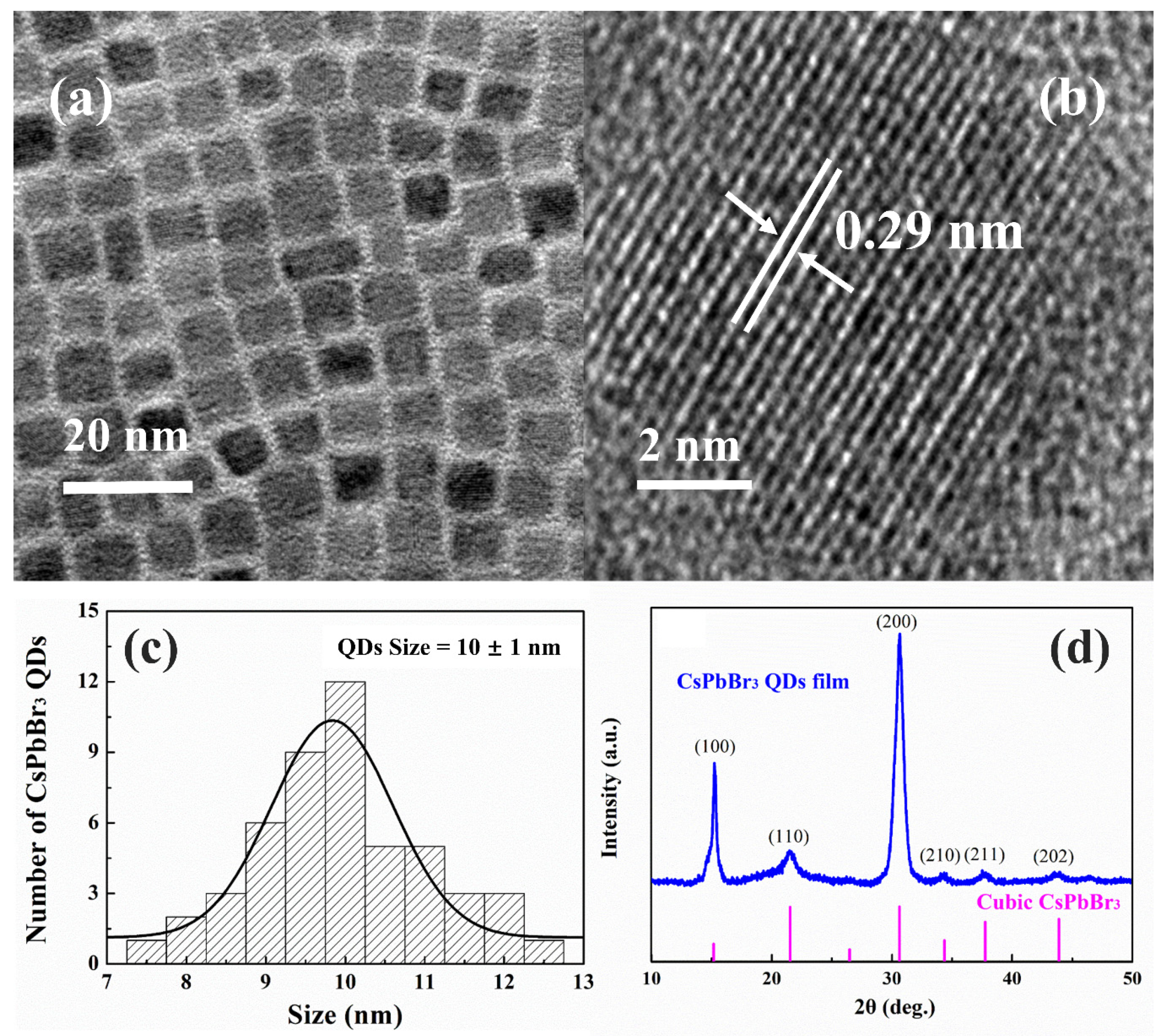
3.1. Structural Characterizations of CsPbBr3 QDs

Figure 1a shows that CsPbBr3 QDs prepared in the current experiment present cubic shapes with a uniform size. The high-resolution TEM (HRTEM) image of one CsPbBr3 QD is presented in Figure 1b. The prepared CsPbBr3 QDs have a crystalline interplanar spacing of 0.29 nm relative to the (200) crystalline planes of cubic CsPbBr3. The distribution of CsPbBr3 QDs sizes is demonstrated in Figure 1c. The quantum confinement effect of CsPbBr3 QDs is expectable since their mean size (about 10 nm) approaches the Bohr diameter (7 nm) that was predicted by the Wannier-Mott excitons of bulk CsPbBr3 perovskites [35]. The pattern of XRD presented in Figure 1d further confirms the cubic crystalline structures of prepared CsPbBr3 QDs. Characteristic diffraction peaks at 15.2°, 21.5°, 30.6°, 34.3°, 37.7°, and 43.8° can be allocated to diffractions from (100), (110), (200), (210), (211), and (202) crystalline planes of cubic CsPbBr3 (JCPDS Card No. 54-0752), respectively, which is aligned with TEM results.

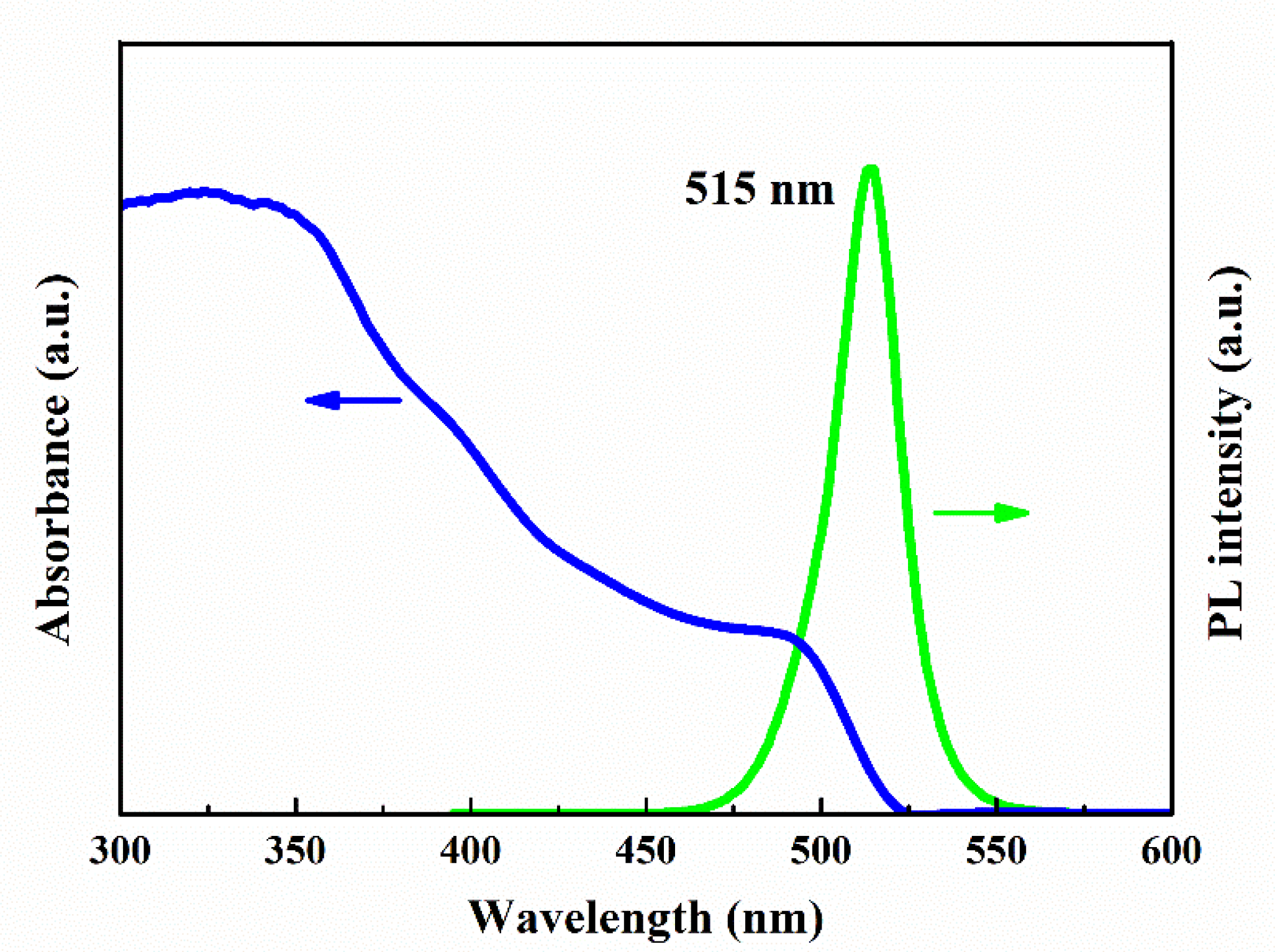
3.2. Optical Properties of CsPbBr3 QDs

It can be seen in Figure 2 that CsPbBr3 QDs have quite high absorbance in the region of short wavelength and the absorption edge locates at 520 nm (2.38 eV), suggesting that the blue-shift of the bandgap corresponds to bulk CsPbBr3 with 2.25 eV [36], which accords with the quantum confinement effect. In addition, the PL spectrum of CsPbBr3 QDs excited by a He-Cd laser of 325 nm is also presented in Figure 2, showing an intense peak at 515 nm with width as narrow as 20 nm at half height. The observed high intensity and color purity PL can be attributed to the uniform size distribution of CsPbBr3 QDs, as identified by TEM measurements. Moreover, the PL QY is measured to be as high as 80%, by using standard fluorescence dye as a reference. It is demonstrated that CsPbBr3 QDs can strongly absorb the near UV photons and then efficiently emit visible light, indicating their suitable down-shifting applications.

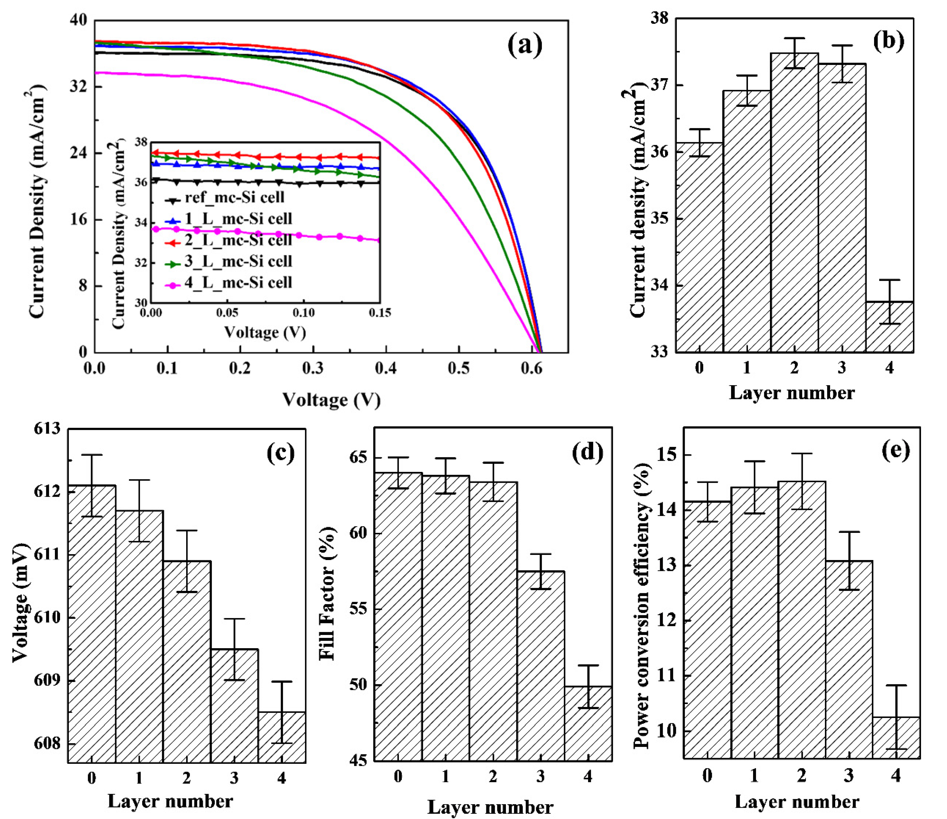
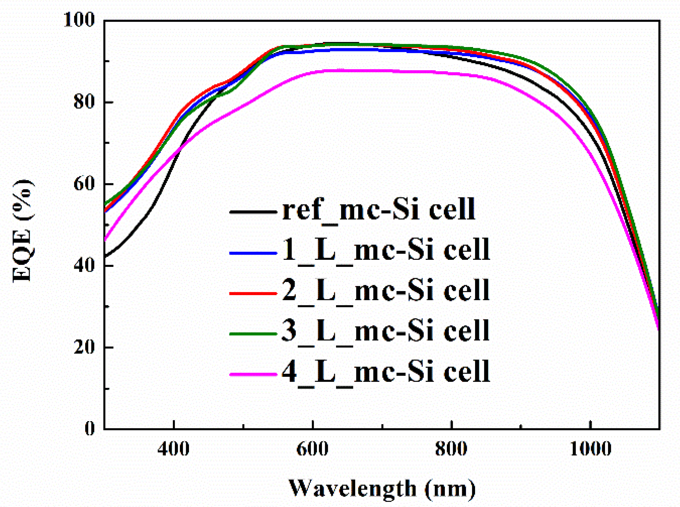
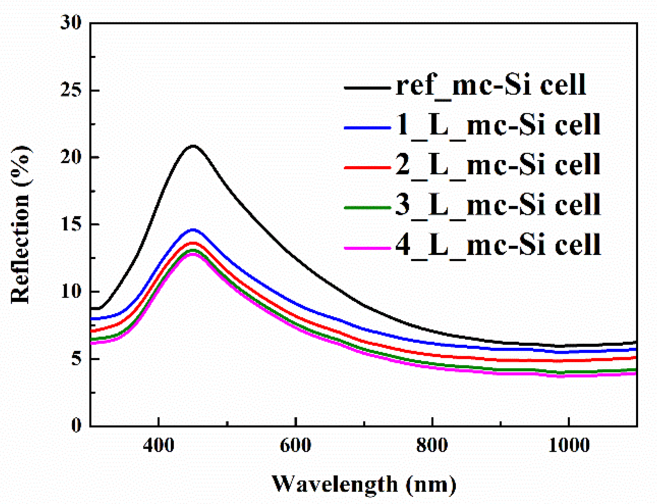
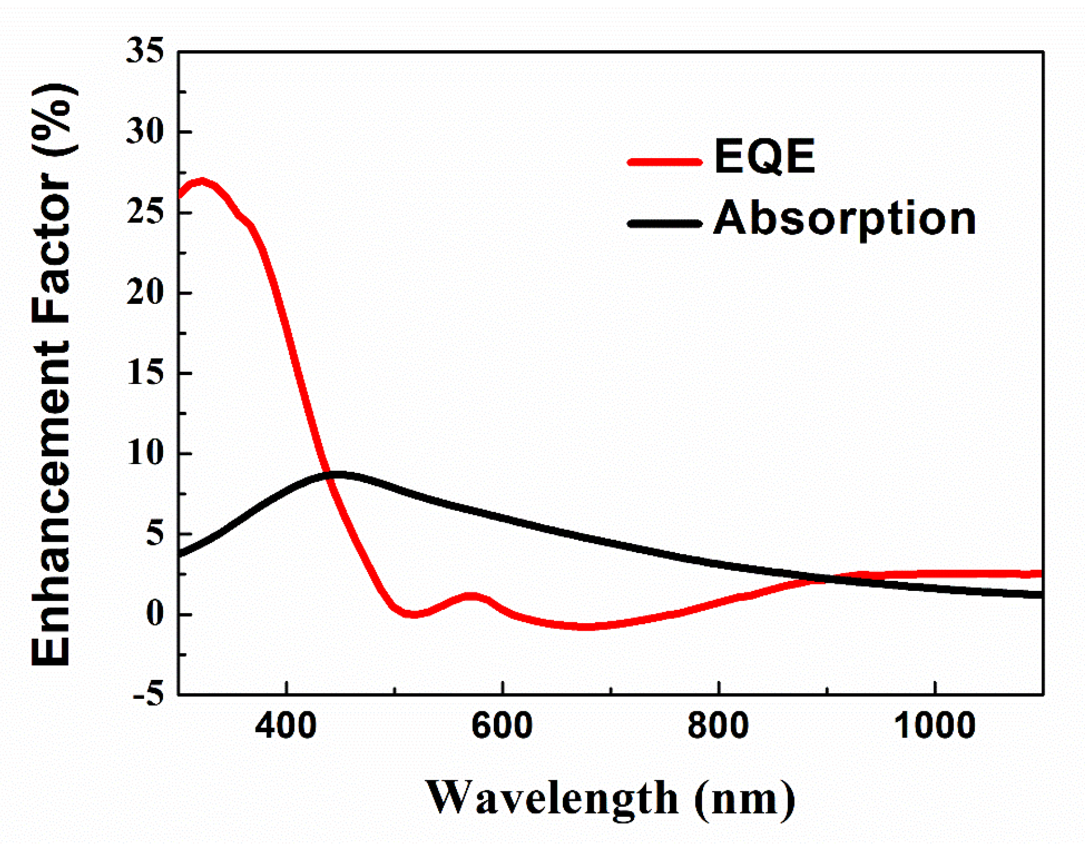
3.3. Photovoltaic Properties of CsPbBr3 QDs/mc-Si Hybrid Structured Solar Cells

CsPbBr3 QDs/mc-Si hybrid structured solar cells were fabricated after spin-coating the colloidal CsPbBr3 QDs solution onto the surface of mc-Si solar cells. Measurements were carried out for the J-V characteristics of solar cells under the AM 1.5 illumination. Figure 3a shows the illuminated J-V curves of mc-Si solar cells inclusive and exclusive of CsPbBr3 QDs. The photovoltaic parameters, including short circuit current density (Jsc), open circuit voltage (Voc), fill factor (FF), and PCE, are summarized as shown in Figure 3b–e. To simplify statement, the CsPbBr3 QDs/mc-Si hybrid structured solar cells are named as 1_L_mc-Si cell, 2_L_mc-Si cell, 3_L_mc-Si cell, and 4_L_mc-Si cell corresponding to the layers of spin-coated CsPbBr3 QDs. Besides, the mc-Si solar cell without CsPbBr3 QDs is named as ref_mc-Si cell for reference.
In general, cell performances strongly depend on the layer number of CsPbBr3 QDs. As shown in Figure 3b, CsPbBr3 QDs/mc-Si hybrid structured solar cells have higher Jsc compared with ref_mc-Si solar cell when the layer number of CsPbBr3 QDs is one to three. In particular, Jsc increases from 36.14 mA/cm2 to 37.48 mA/cm2 when the layer number is two, which is considered to result from better spectral utilization. However, the Jsc of 4_L_mc-Si cell drops to 33.76 mA/cm2, even below that of mc-Si solar cell without CsPbBr3 QDs. In principle, the significant reduction of Jsc can be explained by the following two reasons. The first reason should be the induced contact resistance in CsPbBr3 QDs layers. As we know, undoped CsPbBr3 QDs have poor electrical conductivity. Through the room temperature Hall Effect measurement, the CsPbBr3 QDs film has a dark conductivity of about 3.6 × 10⁻⁷ S/cm, which is very low in the order of magnitude according to the previous reports of metal halide perovskite materials [37,38,39]. In this study, Jsc drops off due to the increase of contact resistance, which deteriorates the carrier collection efficiency. The other reason is the defect in hybrid structures which acts as a non-radiative recombination center and results in thermal energy loss. In order to confirm the existence and study the behavior of defects in hybrid structures, a liquid He-cooled spectrometer of Bruker EMX 10/12+ whose center field is 3342.5 G is used to obtain the low-temperature X-band ESR spectrum of CsPbBr3 QDs/mc-Si structure, as shown in Figure 4. The X-band ESR spectrum at 4 K shows an ESR signal with g = 2.006. In previous works, this signal was usually observed in disordered materials and corresponding to the dangling bond defects derived from the chemical synthesis and spin-coating process, and poor adhesion of coating films on substrates [40,41,42]. It is worth noting that no ESR signal can be detected in the ref_mc-Si solar cell. As a result, the ESR signal here results from the lone-pair electrons (like dangling bonds defects) on the surface and interfaces of CsPbBr3 QDs layers. The density of induced surface and interface defects increases with the increasing layer number of CsPbBr3 QDs, indicating a decline in the Jsc of solar cells because of the enhanced carrier recombination.
As shown in Figure 3c, the change of Voc with the layer number of CsPbBr3 QDs tends to be linear. When the layer number increases, Voc decreases slightly from 612.1 to 608.5 mV because of the surface and interface defects induced by CsPbBr3 QDs layers. As shown in Figure 3d, FF declines obviously when the layer number increases to four, which may be owing to an increase in series resistance (Rs). A negative correlation is found between FF and Rs. Equation (1) below displays the relationship between the voltage and current density of a single-diode model:
J = J 0 ( e x p ( q ( V R s J ) n k B T ) 1 ) + V R s J R s h J p
wherein, J0 and Jp are saturation current density and photocurrent density, respectively, Rs represents series resistance, Rsh represents shunt resistance, n refers to ideality factor, q is electron charge, kB is Boltzmann constant and T is temperature. The Rs values of ref_mc-Si and 4_L_mc-Si cells extracted by a fit to the illuminated J-V curves are 1.2 and 2.8 Ω, respectively. As discussed before, contact resistance increases with the increasing layer number of CsPbBr3 QDs, which in turn give rise to an obvious decline in FF. Finally, the optimal mc-Si solar cell coated with two layers of CsPbBr3 QDs leads to the best PCE of 14.52%, as shown in Figure 3e.
The EQE spectra of mc-Si solar cells inclusive and exclusive of CsPbBr3 QDs layers were measured to further study the down-shifting mechanism of CsPbBr3 QDs/mc-Si hybrid structured solar cells. As observed in Figure 5, the EQE of CsPbBr3 QDs/mc-Si hybrid structured solar cells has a great increase within the spectral range of 300 to 500 nm when the layer number of CsPbBr3 QDs is 1 to 3, which should be attributed to the formation of CsPbBr3 QDs, as discussed before. It suggests that CsPbBr3 QDs are capable of absorbing the near UV light and emitting photons in the region of visible light, which could enhance the spectral response in the region of short wavelength through the re-absorption of mc-Si substrates. When the layer number increases to 4, nevertheless, EQE decreases obviously almost in the whole spectral range, even below that of ref_mc-Si cell, which agrees with the J-V results. Another interesting finding is that the EQE of CsPbBr3 QDs/mc-Si hybrid structured solar cells also increases within the spectral range of 700 to 1100 nm, which will be discussed below. Based on EQE results, Jsc contributed from the spectral response of solar cells in different wavelength ranges can be calculated according to Equation (2) as follows:
J s c = λ 1 λ 2 F ( λ ) · E Q E ( λ ) E ( λ ) d λ
wherein, F ( λ ) and E ( λ ) are incident light flux and energy of photons with the wavelength of λ , respectively. Compared with ref_mc-Si cell, the Jsc of 2_L_mc-Si cell contributed from spectral response within spectral range of 300 to 500 nm and 700 to 1100 nm increases from 5.98 mA/cm2 to 6.79 mA/cm2 and 14.15 mA/cm2 to 14.52 mA/cm2, respectively. As reported by the work of Pi et al., the anti-reflection of prepared porous Si QDs films improved the efficiency of crystalline Si (c-Si) solar cells [43]. In this study, the reflection characteristics of mc-Si solar cells inclusive and exclusive of CsPbBr3 QDs layers must be taken into consideration.
Figure 6 shows the optical reflection (R) spectra of mc-Si solar cells and CsPbBr3 QDs/mc-Si hybrid structured solar cells. Obviously, CsPbBr3 QDs layers lead to the decrease of reflection within the spectral ranges of both 300 to 500 nm and 700 to 1100 nm. The reduction of reflection in long wavelength region is mainly induced by the nanostructure of CsPbBr3 QDs layers. Meanwhile, a greater decline in reflection in short wavelength region should be ascribed to the anti-reflection property of nanostructures and the absorption of CsPbBr3 QDs themselves, as shown in Figure 2.
In order to evaluate the contributions from the down-shifting and anti-reflection effect, an enhancement factor (EF) is defined for both the EQE and absorption results:
E F E Q E = E Q E w i t h   Q D s E Q E w i t h o u t   Q D s E Q E w i t h o u t   Q D s
E F A = A w i t h   Q D s A w i t h o u t   Q D s A w i t h o u t   Q D s
wherein, A is the optical absorption of hybrid structures, which can be deduced by A = 1 − R. Figure 7 shows the EF of 2_L_mc-Si cell as a function of wavelength. It can be clearly seen that the decrease of reflection (which means the enhancement of absorption) improves EQE within the wavelength range of 700 to 1100 nm. However, in wavelength range of 300 to 450 nm, the anti-reflection effect cannot overlap with all the enhancement of EQE result. For example, at 320 nm, the EQE enhancement is 27% while the absorption enhancement is only 4%, which indicates that the down-shifting effect of CsPbBr3 QDs dominates the improving spectral response in the short wavelength region. In contrast, at 480 nm, the CsPbBr3 QDs/mc-Si structures show the strongest anti-reflection property. The enhancements of EQE and absorption are almost the same. Hence, the EQE enhancement is mainly due to the anti-reflection of hybrid structures. In a word, we conclude that the improved photovoltaic performances can be attributed both to the down-shifting effect and the anti-reflection property of CsPbBr3 QDs by forming CsPbBr3 QDs/mc-Si hybrid structures. Furthermore, for future photovoltaic application, in order to avoid the environmental pollution caused by lead, a protected layer will be introduced into the hybrid structures to reduce the lead leakage [44,45].

4. Conclusions

In conclusion, CsPbBr3 QDs are fabricated with a colloidal synthesis approach. TEM and XRD measurements reveal that cubic CsPbBr3 QDs are formed with an average size of 10 nm. It is observed that CsPbBr3 QDs can strongly absorb the near UV light and present a room temperature PL peak at 515 nm, suggesting their typical down-shifting mechanism. Moreover, CsPbBr3 QDs/mc-Si hybrid structured solar cells containing CsPbBr3 QDs of different layers are fabricated. According to the findings, the EQE of CsPbBr3 QDs/mc-Si hybrid structured solar cells is increased within the wavelength ranges of both 300 to 500 nm and 700 to 1100 nm compared with mc-Si solar cells without CsPbBr3 QDs, which should be attributed to the broadband anti-reflection characteristics of nanostructures and the additionally improved down-shifting effect of CsPbBr3 QDs. However, the higher contact resistance and density of surface and interface defects resulting from the increasing layer number of CsPbBr3 QDs deteriorate cell performances due to the reduction of carrier collection efficiency. As a result, the optimal mc-Si solar cell coated with two layers of CsPbBr3 QDs contributes to achieving the best PCE of 14.52%. It is worth noting that all inorganic CsPbBr3 QDs have better stability than the organic-inorganic (MAPbBr3) perovskite materials. Our experimental results indicate a promising way to exploit CsPbBr3 QDs for future photovoltaic devices.

Author Contributions

Conceptualization, Y.C. and J.X.; methodology, Y.C., D.W., and P.Z.; investigation, Y.C., D.W., and D.S.; writing—original draft preparation, Y.C.; writing—review and editing, X.Z.; funding acquisition, Y.C. and D.S. All authors have read and agreed to the published version of the manuscript.

Funding

This research was funded by NSFC (No. 61704148), NSF of Jiangsu Province (No. BK20170514), NSF of Jiangsu Higher Education Institutions (No. 17KJB140030), NSF of Yangzhou City (No. YZ2017102), Open project of state key laboratory of solid state microstructure physics (Nos. M30039, M31037), China Postdoctoral Science Foundation (No. 2019M651750), “Qing Lan project” of Jiangsu Province, Postdoctoral research grant program of Jiangsu Province, Overseas training program for excellent young and middle-aged teachers and principals of universities in Jiangsu Province, and Special Fund for City School Cooperation of Yangzhou City (No. SSX2018000001).

Conflicts of Interest

The authors declare no conflict of interest.

References

  1. Zhao, J.H.; Wang, A.H.; Green, M.A. 24.5% Efficiency silicon PERT cells on MCZ substrates and 24.7% efficiency PERL cells on FZ substrates. Prog. Photovolt. Res. Appl. 1999, 7, 471–474. [Google Scholar] [CrossRef]
  2. Takatsuka, H.; Noda, M.; Yonekura, Y.; Takeuchi, Y.; Yamauchi, Y. Development of high efficiency large area silicon thin film modules using VHF-PECVD. Sol. Energy 2004, 77, 951–960. [Google Scholar] [CrossRef]
  3. Hu, L.; Chen, G. Analysis of optical absorption in silicon nanowire arrays for photovoltaic applications. Nano Lett. 2007, 7, 3249–3252. [Google Scholar] [CrossRef]
  4. Clement, F.; Menkoe, M.; Erath, D.; Kubera, T.; Hoenig, R.; Kwapil, W.; Wolke, W.; Biro, D.; Preu, R. High throughput via-metallization technique for multi-crystalline metal wrap through (MWT) silicon solar cells exceeding 16% efficiency. Sol. Energy Mater. Sol. Cells 2010, 94, 51–56. [Google Scholar] [CrossRef]
  5. Shockley, W.; Queisser, H.J. Detailed balance limit of efficiency of p-n junction solar cells. J. Appl. Phys. 1961, 32, 510–519. [Google Scholar] [CrossRef]
  6. Slooff, L.H.; Kinderman, R.; Burgers, A.R.; Bakker, N.J.; van Roosmalen, J.A.M.; Büchtemann, A.; Danz, R.; Schleusener, M. Efficiency enhancement of solar cells by application of a polymer coating containing a luminescent dye. J. Sol. Energy Eng. 2007, 129, 272–276. [Google Scholar] [CrossRef]
  7. Huang, C.Y.; Wang, D.Y.; Wang, C.H.; Chen, Y.T.; Wang, Y.T.; Jiang, Y.T.; Yang, Y.J.; Chen, C.C.; Chen, Y.F. Efficient light harvesting by photon downconversion and light trapping in hybrid ZnS nanoparticles/Si nanotips solar cells. ACS Nano 2010, 4, 5849–5854. [Google Scholar] [CrossRef]
  8. Stupca, M.; Alsalhi, M.; Saud, T.A.; Almuhanna, A.; Nayfeh, M.H. Enhancement of polycrystalline silicon solar cells using ultrathin films of silicon nanoparticle. Appl. Phys. Lett. 2007, 91, 063107. [Google Scholar] [CrossRef]
  9. Cheng, Z.; Su, F.; Pan, L.; Cao, M.; Sun, Z. CdS quantum dot-embedded silica film as luminescent down-shifting layer for crystalline Si solar cells. J. Alloys Compd. 2010, 494, 7–10. [Google Scholar] [CrossRef]
  10. Sheng, X.; Corcoran, C.J.; He, J.W.; Shen, L.; Kim, S.; Park, J.; Nuzzo, R.G.; John, A.; Rogers, J.A. Enhanced ultraviolet responses in thin-film InGaP solar cells by down-shifting. Phys. Chem. Chem. Phys. 2013, 15, 20434–20437. [Google Scholar] [CrossRef]
  11. Nam, W.I.; Kang, E.K.; Park, H.G.; Jun, D.H.; Song, Y.M. Luminescent coverglass for improved absorption efficiency in III–V photovoltaic modules. Electron. Lett. 2016, 52, 1891–1892. [Google Scholar] [CrossRef]
  12. Yoon, J.; Li, L.; Semichaevsky, A.; Ryu, J.H.; Johnson, H.T.; Nuzzo, R.G.; Rogers, J.A. Flexible concentrator photovoltaics based on microscale silicon solar cells embedded in luminescent waveguides. Nat. Commun. 2011, 2, 343. [Google Scholar] [CrossRef]
  13. Van Sark, W.; Meijerink, A.; Schropp, R.; van Roosmalen, J.; Lysen, E.H. Enhancing solar cell efficiency by using spectral converters. Sol. Energy Mater. Sol. Cells 2005, 87, 395–409. [Google Scholar] [CrossRef] [Green Version]
  14. Pi, X.D.; Zhang, L.; Yang, D.R. Enhancing the efficiency of multicrystalline silicon solar cells by the inkjet printing of silicon-quantum-dot ink. J. Phys. Chem. C 2012, 116, 21240–21243. [Google Scholar] [CrossRef]
  15. Zhu, M.; Peng, X.; Wang, Z.; Bai, Z.; Chen, B.; Wang, Y.; Hao, H.; Shao, Z.; Zhong, H. Highly transparent and colour-tunable composite films with increased quantum dot loading. J. Mater. Chem. C 2014, 2, 10031–10036. [Google Scholar] [CrossRef]
  16. Priolo, F.; Gregorkiewicz, T.; Galli, M.; Krauss, T.F. Silicon nanostructures for photonics and photovoltaics. Nat. Nanotechnol. 2014, 9, 19–32. [Google Scholar] [CrossRef]
  17. Prezioso, S.; Anopchenko, A.; Gaburro, Z.; Pavesi, L.; Pucker, G.; Vanzetti, L.; Bellutti, P. Electrical conduction and electroluminescence in nanocrystalline silicon-based light emitting devices. J. Appl. Phys. 2008, 104, 063103. [Google Scholar] [CrossRef]
  18. Luo, J.W.; Li, S.S.; Sychugov, I.; Pevere, F.; Linnros, J.; Zunger, A. Absence of redshift in the direct bandgap of silicon nanocrystals with reduced size. Nat. Nanotechnol. 2017, 12, 930–932. [Google Scholar] [CrossRef]
  19. Zhang, X.Y.; Lin, H.; Huang, H.; Reckmeier, C.; Zhang, Y.; Choy, W.C.H.; Rogach, A.L. Enhancing the brightness of cesium lead halide perovskite nanocrystal based green light-emitting devices through the interface engineering with perfluorinated ionomer. Nano Lett. 2016, 16, 1415–1420. [Google Scholar] [CrossRef]
  20. Bao, J.; Hadjiev, V.G. Origin of luminescent centers and edge states in low-dimensional lead halide perovskites: Controversies, challenges and instructive approaches. Nano-Micro Lett. 2019, 11, 26. [Google Scholar] [CrossRef] [Green Version]
  21. Kovalenko, M.V.; Protesescu, L.; Bodnarchuk, M.I. Properties and potential optoelectronic applications of lead halide perovskite nanocrystals. Science 2017, 358, 745–750. [Google Scholar] [CrossRef] [Green Version]
  22. Yakunin, S.; Protesescu, L.; Krieg, F.; Bodnarchuk, M.I.; Nedelcu, G.; Humer, M.; Luca, G.D.; Fiebig, M.; Heiss, W.; Kovalenko, M.V. Low-threshold amplified spontaneous emission and lasing from colloidal nanocrystals of cesium lead halide perovskites. Nat. Commun. 2015, 6, 8056. [Google Scholar] [CrossRef]
  23. Wang, Y.; Li, X.M.; Song, J.Z.; Xiao, L.; Zeng, H.B.; Sun, H.D. All-inorganic colloidal perovskite quantum dots: A new class of lasing materials with favorable characteristics. Adv. Mater. 2015, 2, 7101–7108. [Google Scholar] [CrossRef]
  24. Hu, F.R.; Zhang, H.C.; Sun, C.; Yin, C.Y.; Lv, B.H.; Zhang, C.F.; Yu, W.W.; Wang, X.Y.; Zhang, Y.; Xiao, M. Superior optical properties of perovskite nanocrystals as single photon emitters. ACS Nano 2015, 9, 12410–12416. [Google Scholar] [CrossRef] [Green Version]
  25. Zhang, J.; Yang, X.K.; Deng, H.; Qiao, K.K.; Farooq, U.; Ishaq, M.; Yi, F.; Liu, H.; Tang, J.; Song, H.S. Low-dimensional halide perovskites and their advanced optoelectronic applications. Nano-Micro Lett. 2017, 9, 36. [Google Scholar] [CrossRef] [PubMed] [Green Version]
  26. Kwak, D.H.; Lim, D.H.; Ra, H.S.; Ramasamy, P.; Lee, J.S. High performance hybrid graphene-CsPbBr3-xIx perovskite nanocrystal photodetector. RSC Adv. 2016, 6, 65252–65256. [Google Scholar] [CrossRef]
  27. Ramasamy, P.; Lim, D.H.; Kim, B.; Lee, S.H.; Lee, M.S.; Lee, J.S. All-inorganic cesium lead halide perovskite nanocrystals for photodetector applications. Chem. Commun. 2016, 52, 2067–2070. [Google Scholar] [CrossRef] [PubMed]
  28. Sadhanala, A.; Ahmad, S.; Zhao, B.; Giesbrecht, N.; Pearce, P.M.; Deschler, F.; Hoye, R.L.Z.; Gödel, C.; Bein, T.; Docampo, P.; et al. Blue-green color tunable solution processable organolead chloride-bromide mixed halide perovskites for optoelectronic applications. Nano Lett. 2015, 15, 6095–6101. [Google Scholar] [CrossRef] [Green Version]
  29. Hossain, M.I.; Qarony, W.; Ma, S.; Zeng, L.H.; Knipp, D.; Tsang, Y.H. Perovskite/silicon tandem solar cells: From detailed balance limit calculations to photon management. Nano-Micro Lett. 2019, 11, 58. [Google Scholar] [CrossRef] [Green Version]
  30. Nedelcu, G.; Protesescu, L.; Yakunin, S.; Bodnarchuk, M.I.; Grotevent, M.J.; Kovalenko, M.V. Fast anion-exchange in highly luminescent nanocrystals of cesium lead halide perovskites (CsPbX3, X = Cl, Br, I). Nano Lett. 2015, 15, 5635–5640. [Google Scholar] [CrossRef]
  31. Mastronardi, M.L.; Flaig, F.M.; Faulkner, D.; Henderson, E.J.; Kubel, C.; Lemmer, U.; Ozin, G.A. Size-dependent absolute quantum yields for size-separated colloidally-stable Silicon nanocrystals. Nano Lett. 2012, 12, 337. [Google Scholar] [CrossRef]
  32. Liu, X.; Zhang, Y.; Yu, T.; Qiao, X.; Gresback, R.; Pi, X.; Yang, D. Optimum quantum yield of the light emission from 2 to 10 nm hydrosilylated Silicon quantum dots. Part. Part. Syst. Charact. 2016, 33, 44–52. [Google Scholar] [CrossRef]
  33. Li, X.M.; Wu, Y.; Zhang, S.L.; Cai, B.; Gu, Y.; Song, J.Z.; Zeng, H.B. CsPbX3 quantum dots for lighting and displays: Room temperature synthesis, photoluminescence superiorities, underlying origins and white light-emitting diodes. Adv. Funct. Mater. 2016, 15, 2435–2445. [Google Scholar] [CrossRef]
  34. Kim, Y.C.; Jeong, H.J.; Kim, S.T.; Song, Y.H.; Kim, B.Y.; Kim, J.P.; Kang, B.K.; Yun, J.Y.; Jang, J.H. Luminescent down-shifting CsPbBr3 perovskite nanocrystals for flexible Cu(In,Ga)Se2 solar cells. Nanoscale 2020, 12, 558–562. [Google Scholar] [CrossRef] [PubMed] [Green Version]
  35. Protesescu, L.; Yakunin, S.; Bodnarchuk, M.I.; Krieg, F.; Caputo, R.; Hendon, C.H.; Yang, R.X.; Walsh, A.; Kovalenko, M.V. Nanocrystals of cesium lead halide perovskites (CsPbX3, X = Cl, Br, and I): Novel optoelectronic materials showing bright emission with wide color gamut. Nano Lett. 2015, 15, 3692–3696. [Google Scholar] [CrossRef] [PubMed] [Green Version]
  36. Stoumpos, C.C.; Malliakas, C.D.; Peters, J.A.; Liu, Z.; Sebastian, M.; Im, J.; Chasapis, T.C.; Wibowo, A.C.; Chung, D.Y.; Freeman, A.J.; et al. Crystal growth of the perovskite semiconductor CsPbBr3: A new material for high-energy radiation detection. Cryst. Growth Des. 2013, 13, 2722–2727. [Google Scholar] [CrossRef]
  37. Palazon, F.; Di Stasio, F.; Lauciello, S.; Krahne, R.; Prato, M.; Manna, L. Evolution of CsPbBr3 nanocrystals upon post-synthesis annealing under an inert atmosphere. J. Mater. Chem. C 2016, 4, 9179–9182. [Google Scholar] [CrossRef] [Green Version]
  38. Mao, X.L.; Qiu, T.; Zhang, S.F.; Ma, H.; Hu, Y.Q.; Bai, F.; Wu, Z.C. Air-stable CsPb1-xBixBr3 (0 ≤ x. J. Mater. Chem. C 2017, 5, 4931–4939. [Google Scholar]
  39. Zhang, H.J.; Liu, X.; Dong, J.P.; Yu, H.; Zhou, C.; Zhang, B.B.; Xu, Y.D.; Jie, W.Q. Centimeter-szed inorganic lead halide perovskite CsPbBr3 crystals grown by an improved solution method. Cryst. Growth Des. 2017, 17, 6426–6431. [Google Scholar] [CrossRef]
  40. Gong, X.; Guan, L.; Pan, H.P.; Sun, Q.; Zhao, X.J.; Li, H.; Pan, H.; Shen, Y.; Shao, Y.; Sun, L.J.; et al. Highly efficient perovskite solar cells via Nickel passivation. Adv. Funct. Mater. 2018, 28, 1804286. [Google Scholar] [CrossRef]
  41. Náfrádi, B.; Szirmai, P.; Spina, M.; Lee, H.; Yazyev, O.; Arakcheeva, A.; Chernyshov, D.; Gibert, M.; Forró, L.; Horváth, E. Optically switched magnetism in photovoltaic perovskite CH3NH3(Mn:Pb)I3. Nat. Commun. 2016, 7, 13406. [Google Scholar] [CrossRef] [PubMed] [Green Version]
  42. Zhou, Y.; Yong, Z.J.; Zhang, K.C.; Liu, B.M.; Wang, Z.W.; Hou, J.S.; Fang, Y.Z.; Zhou, Y.; Sun, H.T.; Song, B. Ultrabroad photoluminescence and electroluminescence at new wavelengths from doped organometal halide perovskites. J. Phys. Chem. Lett. 2016, 7, 2735–2741. [Google Scholar] [CrossRef] [PubMed]
  43. Pi, X.D.; Li, Q.; Li, D.S.; Yang, D.R. Spin-coating silicon-quantum-dot ink to improve solar cell efficiency. Sol. Energy Mater. Sol. Cells 2011, 95, 2941–2945. [Google Scholar] [CrossRef]
  44. Jiang, Y.; Qiu, L.B.; Juarez-Perez, E.J.; Ono, L.K.; Hu, Z.H.; Liu, Z.H.; Wu, Z.F.; Meng, L.Q.; Wang, Q.J.; Qi, Y.B. Reduction of lead leakage from damaged lead halide perovskite solar modules using self-healing polymer-based encapsulation. Nat. Energy 2019, 4, 585–593. [Google Scholar] [CrossRef]
  45. Li, X.; Zhang, F.; He, H.Y.; Berry, J.J.; Zhu, K.; Xu, T. On-device lead sequestration for perovskite solar cells. Nature 2020, 578, 555–558. [Google Scholar] [CrossRef]
Figure 1. (a) TEM and (b) HRTEM images of CsPbBr3 QDs. (c) Histogram for the size distribution of the CsPbBr3 QDs. (d) XRD spectrum of CsPbBr3 QDs film.
Nanomaterials 10 00775 g001
Figure 2. Optical absorption (blue line) and PL (green line) spectra of CsPbBr3 QDs.
Nanomaterials 10 00775 g002
Figure 3. (a) AM 1.5G illuminated J-V curves of mc-Si solar cells inclusive and exclusive of CsPbBr3 QDs layers. (b) Short circuit current density (Jsc), (c) open circuit voltage (Voc), (d) fill factor (FF), and (e) power conversion efficiency (PCE) of solar cells.
Nanomaterials 10 00775 g003
Figure 4. Low temperature ESR spectrum of the CsPbBr3 QDs/mc-Si structure.
Nanomaterials 10 00775 g004
Figure 5. External quantum efficiency (EQE) spectra of mc-Si solar cells inclusive and exclusive of CsPbBr3 QDs layers.
Nanomaterials 10 00775 g005
Figure 6. Optical reflection spectra of mc-Si solar cells inclusive and exclusive of CsPbBr3 QDs layers.
Nanomaterials 10 00775 g006
Figure 7. Enhancement factor (EF) of mc-Si solar cell coated with two layers of CsPbBr3 QDs as a function of wavelength.
Nanomaterials 10 00775 g007

