Electrical Phase Control Based on Graphene Surface Plasmon Polaritons in Mid-infrared


Abstract
1. Introduction
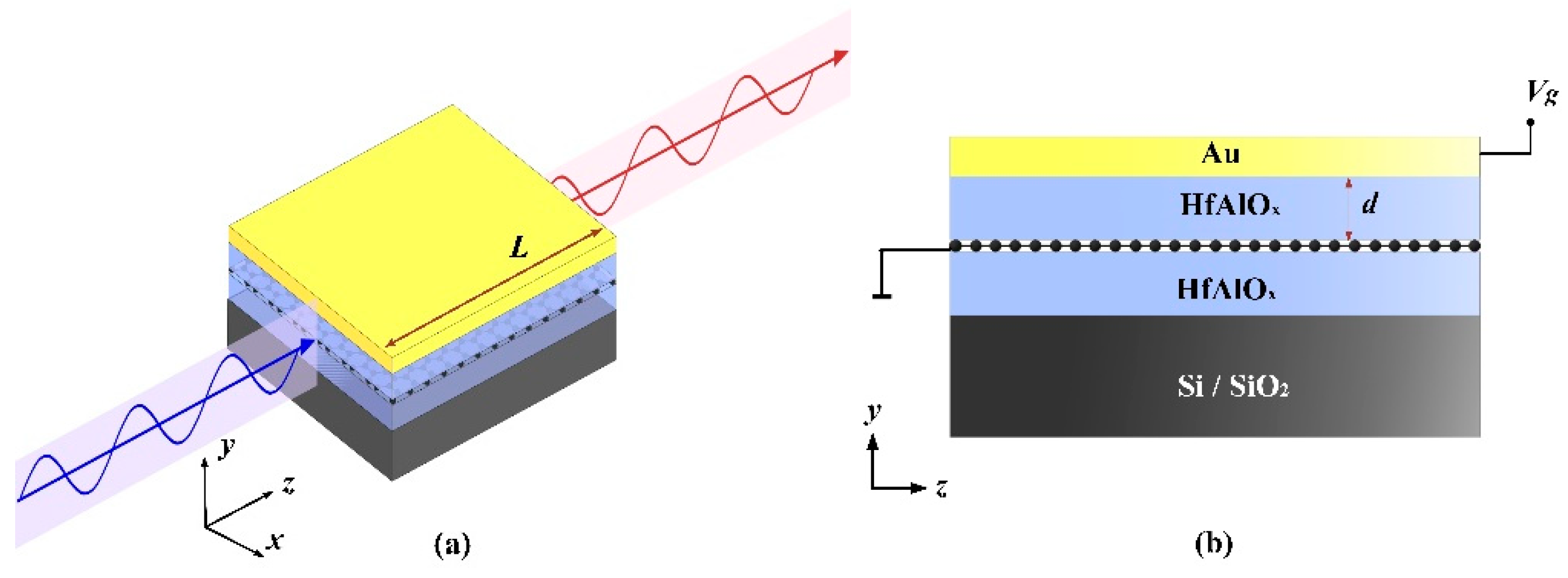
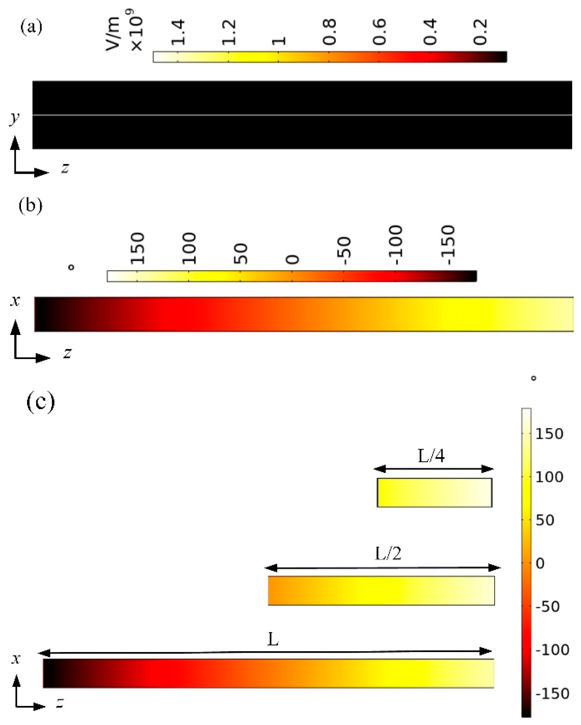
2. Structure Design
3. Methods
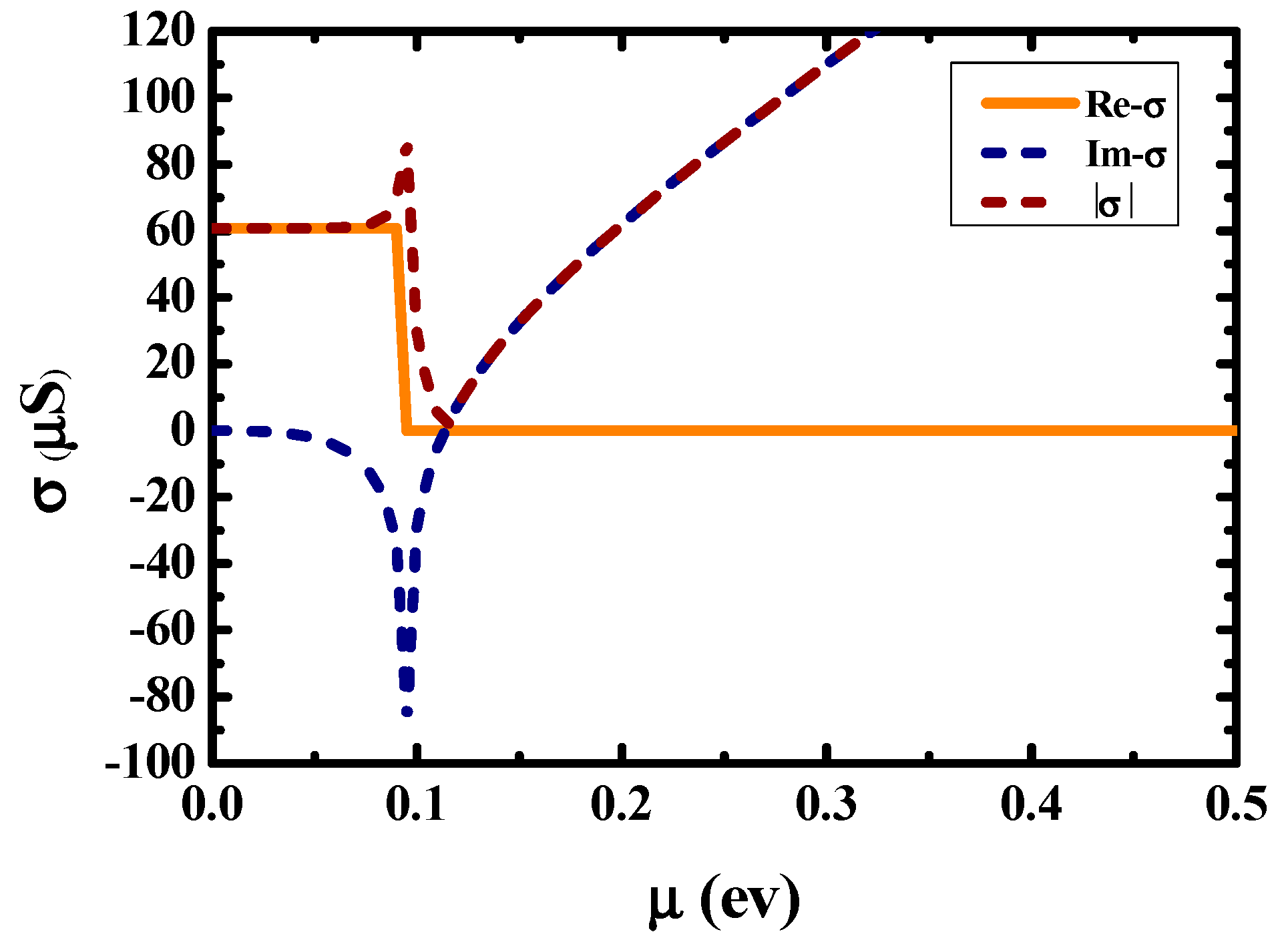
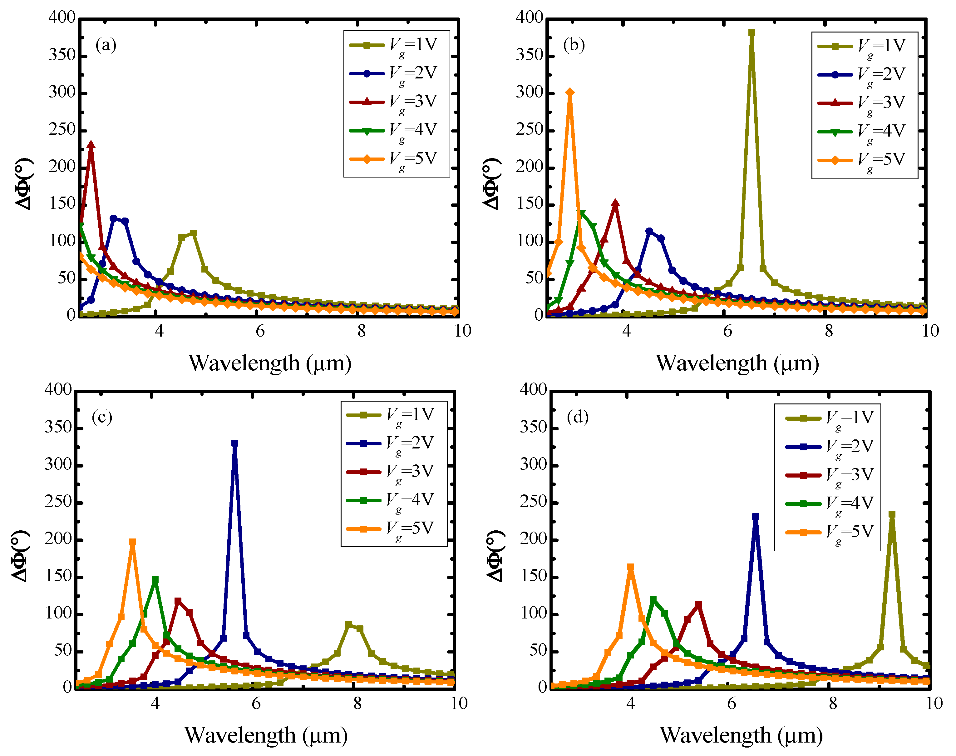
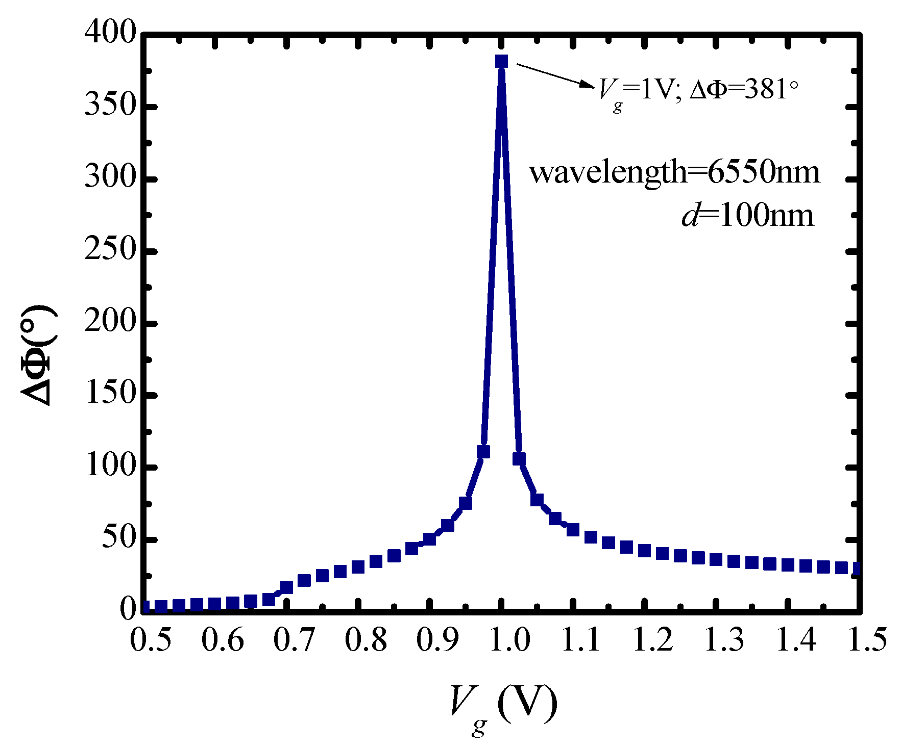
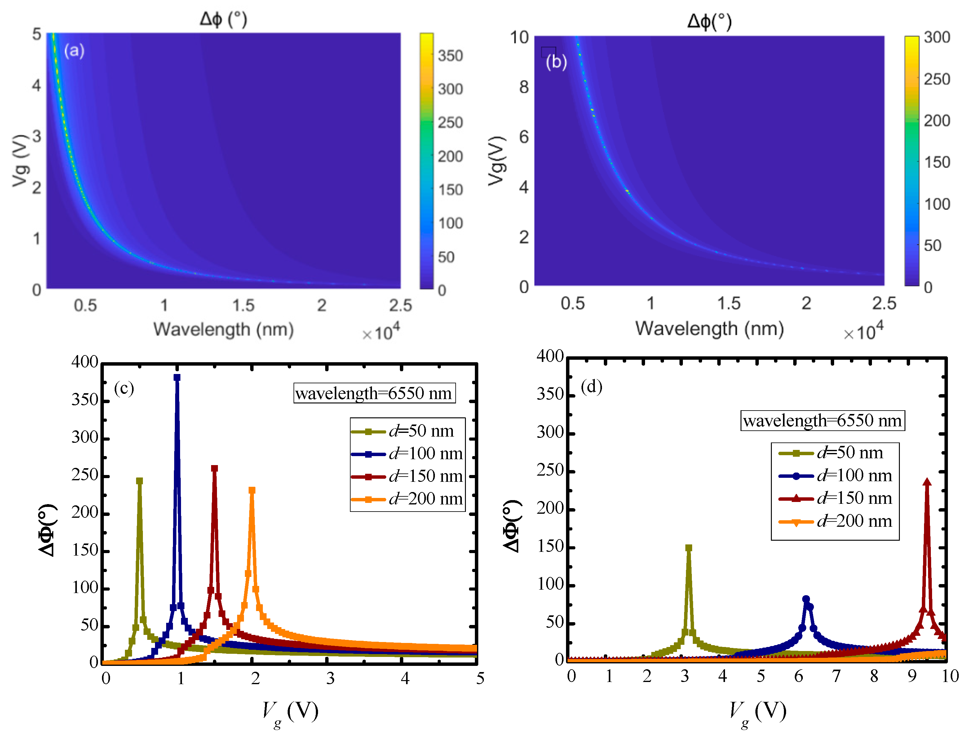
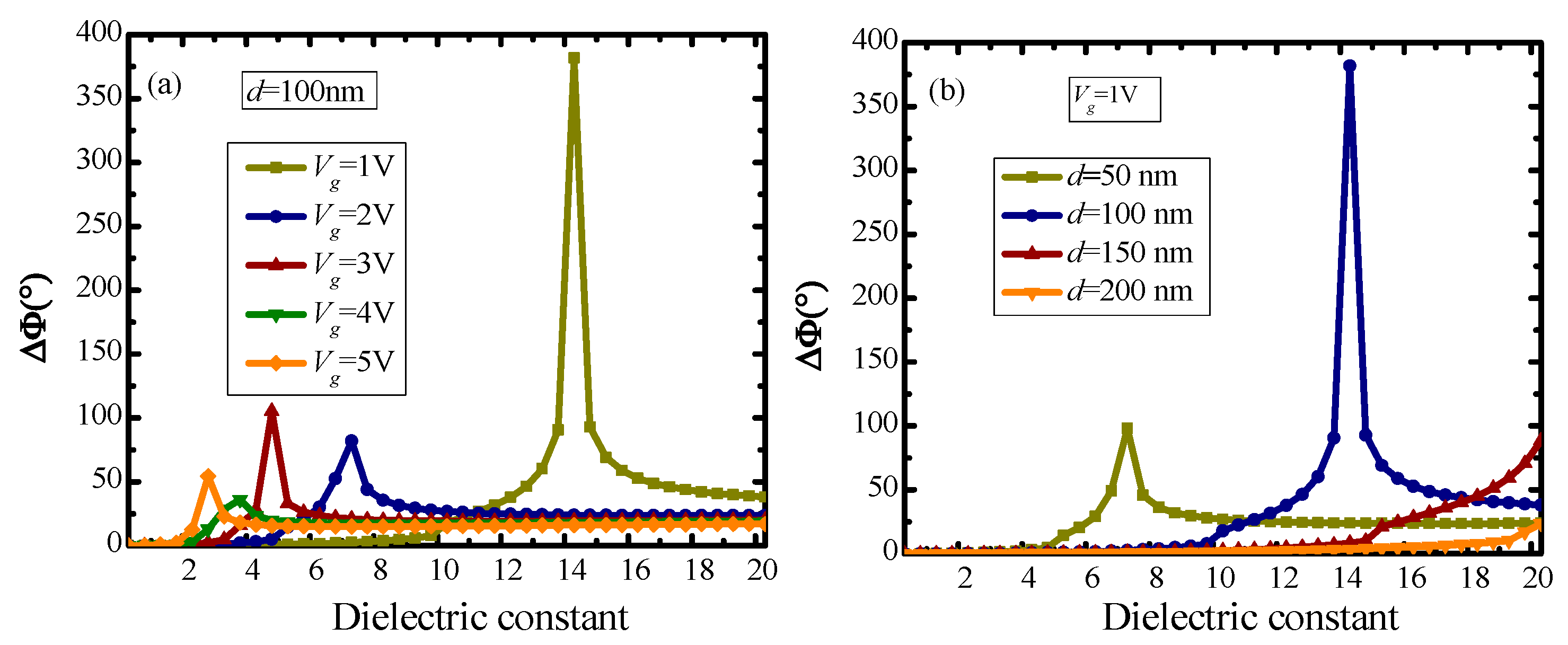
4. Results and Discussion
5. Conclusions
Author Contributions
Funding
Acknowledgments
Conflicts of Interest
References
- Zayats, A.V.; Smolyaninov, I.I.; Maradudin, A.A. Nano-optics of surface plasmon polaritons. Phys. Rep. 2005, 408, 131–314. [Google Scholar] [CrossRef]
- Butt, M.; Khonina, S.; Kazanskiy, N. Enhancement of evanescent field ratio in a silicon strip waveguide by incorporating a thin metal film. Laser Phys. 2019, 29, 076202. [Google Scholar] [CrossRef]
- Butt, M.; Khonina, S.; Kazanskiy, N. Plasmonic refractive index sensor based on metal–insulator-metal waveguides with high sensitivity. J. Mod. Opt. 2019, 66, 1038–1043. [Google Scholar] [CrossRef]
- Butt, M.; Khonina, S.; Kazanskiy, N. Hybrid plasmonic waveguide-assisted Metal–Insulator–Metal ring resonator for refractive index sensing. J. Mod. Opt. 2018, 65, 1135–1140. [Google Scholar] [CrossRef]
- Zhernovnykova, O.A.; Popova, O.; Deynychenko, G.; Deynichenko, T.; Bludov, Y. Surface plasmon-polaritons in graphene, embedded into medium with gain and losses. J. Phys. Condens. Matter. 2019, 31, 465301. [Google Scholar] [CrossRef]
- Su, Y.; Lin, Q.; Zhai, X.; Wang, L.-L. Enhanced Confinement of Terahertz Surface Plasmon Polaritons in Bulk Dirac Semimetal-Insulator-Metal Waveguides. Nanoscale Res. Lett. 2018, 13, 308. [Google Scholar] [CrossRef]
- Chau, Y.-F.; Lin, Y.-J.; Tsai, D.P. Enhanced surface plasmon resonance based on the silver nanoshells connected by the nanobars. Opt. Express 2010, 18, 3510–3518. [Google Scholar] [CrossRef]
- Chau, Y.-F.; Yeh, H.-H.; Liao, C.-C.; Ho, H.-F.; Liu, C.-Y.; Tsai, D.P. Controlling surface plasmon of several pair arrays of silver-shell nanocylinders. Appl. Opt. 2010, 49, 1163–1169. [Google Scholar] [CrossRef]
- Wang, Y.; Wang, S.; Cai, M.; Liu, H. A Long Propagation Distance Hybrid Triangular Prism Waveguide for Ultradeep Subwavelength Confinement. IEEE Sens. J. 2019, 19, 11159–11166. [Google Scholar] [CrossRef]
- Wang, Y.; Liu, H.; Wang, S.; Cai, M.; Ma, L. Optical Transport Properties of Graphene Surface Plasmon Polaritons in Mid-Infrared Band. Crystals 2019, 9, 354. [Google Scholar] [CrossRef]
- Lu, F.; Liu, B.; Shen, S. Infrared wavefront control based on graphene metasurfaces. Adv. Opt. Mater. 2014, 2, 794–799. [Google Scholar] [CrossRef]
- Koppens, F.H.; Chang, D.E.; de Abajo, F.J.G. Graphene plasmonics: A platform for strong light–matter interactions. Nano Lett. 2011, 11, 3370–3377. [Google Scholar] [CrossRef] [PubMed]
- Jablan, M.; Buljan, H.; Soljačić, M. Plasmonics in graphene at infrared frequencies. Phys. Rev. B 2009, 80, 245435. [Google Scholar] [CrossRef]
- Rosa, H.G.; Steinberg, D.; Zapata, J.D.; Saito, L.A.M.; Cárdenas, A.M.; Gomes, J.C.V.; Souza, E.A.T.D. Raman Mapping Characterization of All-Fiber CVD Monolayer Graphene Saturable Absorbers for Erbium-Doped Fiber Laser Mode Locking. J. Lightwave Technol. 2015, 33, 4118–4123. [Google Scholar] [CrossRef]
- Fei, Z.; Andreev, G.O.; Bao, W.; Zhang, L.M.; McLeod, A.S.; Wang, C.; Stewart, M.K.; Zhao, Z.; Dominguez, G.; Thiemens, M. Infrared nanoscopy of Dirac plasmons at the graphene–SiO2 interface. Nano Lett. 2011, 11, 4701–4705. [Google Scholar] [CrossRef] [PubMed]
- Kuzmin, D.A.; Bychkov, I.V.; Shavrov, V.G.; Temnov, V.V. Plasmonics of magnetic and topological graphene-based nanostructures. Nanophotonics 2018, 7, 597–611. [Google Scholar] [CrossRef]
- Xu, Z.; Wu, D.; Liu, Y.; Liu, C.; Yu, Z.; Yu, L.; Ye, H. Design of a tunable ultra-broadband terahertz absorber based on multiple layers of graphene ribbons. Nanoscale Res. Lett. 2018, 13, 143. [Google Scholar] [CrossRef]
- Shan, Y.; Tang, J.; Wu, L.; Lu, S.; Dai, X.; Xiang, Y. Spatial self-phase modulation and all-optical switching of graphene oxide dispersions. J. Alloys. 2019, 771, 900–904. [Google Scholar] [CrossRef]
- Kats, M.A.; Blanchard, R.; Genevet, P.; Yang, Z.; Qazilbash, M.M.; Basov, D.; Ramanathan, S.; Capasso, F. Thermal tuning of mid-infrared plasmonic antenna arrays using a phase change material. Opt. Lett. 2013, 38, 368–370. [Google Scholar] [CrossRef]
- Samolis, P.D.; Sander, M. Phase-sensitive lock-in detection for high-contrast mid-infrared photothermal imaging with sub-diffraction limited resolution. Opt. Express 2019, 27, 2643–2655. [Google Scholar] [CrossRef]
- Sherrott, M.C.; Hon, P.W.; Fountaine, K.T.; Garcia, J.C.; Ponti, S.M.; Brar, V.W.; Sweatlock, L.A.; Atwater, H.A. Experimental demonstration of> 230 phase modulation in gate-tunable graphene–gold reconfigurable mid-infrared metasurfaces. Nano Lett. 2017, 17, 3027–3034. [Google Scholar] [CrossRef] [PubMed]
- Ying, D.; Xie, T.; Wang, Z.; Liu, Q.; Ye, K.; Jin, Z. A closed-loop RFOG based on digital serrodyne and sine modulations with two LiNbO3 phase modulators. Opt. Commun. 2019, 452, 151–157. [Google Scholar] [CrossRef]
- Herzog, B.; Lingnau, B.; Kolarczik, M.; Helmrich, S.; Lüdge, K.; Woggon, U.; Owschimikow, N. Role of Mixed-dimensional Excitons in the Phase Dynamics of Semiconductor Optical Lasers and Amplifiers. In Proceedings of the CLEO: QELS Fundamental Science, (Optical Society of America, 2019), JW2A. 24, San Jose, CA, USA, 5–10 May 2019. [Google Scholar]
- Fei, Z.; Rodin, A.; Andreev, G.O.; Bao, W.; McLeod, A.; Wagner, M.; Zhang, L.; Zhao, Z.; Thiemens, M.; Dominguez, G. Gate-tuning of graphene plasmons revealed by infrared nano-imaging. Nature 2012, 487, 82. [Google Scholar] [CrossRef] [PubMed]
- Li, Z.; Henriksen, E.A.; Jiang, Z.; Hao, Z.; Martin, M.C.; Kim, P.; Stormer, H.; Basov, D.N. Dirac charge dynamics in graphene by infrared spectroscopy. Nat. Phys. 2008, 4, 532. [Google Scholar] [CrossRef]
- Fang, Z.; Thongrattanasiri, S.; Schlather, A.; Liu, Z.; Ma, L.; Wang, Y.; Ajayan, P.M.; Nordlander, P.; Halas, N.J.; de Abajo, F.J.G. Gated tunability and hybridization of localized plasmons in nanostructured graphene. ACS Nano 2013, 7, 2388–2395. [Google Scholar] [CrossRef] [PubMed]
- Jadidi, M.M.; Sushkov, A.B.; Myers-Ward, R.L.; Boyd, A.K.; Daniels, K.M.; Gaskill, D.K.; Fuhrer, M.S.; Drew, H.D.; Murphy, T.E. Tunable terahertz hybrid metal–graphene plasmons. Nano Lett. 2015, 15, 7099–7104. [Google Scholar] [CrossRef]
- Wang, X.; Meng, H.; Deng, S.; Lao, C.; Wei, Z.; Wang, F.; Tan, C.; Huang, X. Hybrid Metal Graphene-Based Tunable Plasmon-Induced Transparency in Terahertz Metasurface. Nanomaterials 2019, 9, 385. [Google Scholar] [CrossRef]
- Mueller, T.; Xia, F.; Freitag, M.; Tsang, J.; Avouris, P. Role of contacts in graphene transistors: A scanning photocurrent study. Phys. Rev. B 2009, 79, 245430. [Google Scholar] [CrossRef]
- Goldflam, M.D.; Ruiz, I.; Howell, S.W.; Wendt, J.R.; Sinclair, M.B.; Peters, D.W.; Beechem, T.E. Tunable dual-band graphene-based infrared reflectance filter. Opt. Express 2018, 26, 8532–8541. [Google Scholar] [CrossRef]
- Casiraghi, C.; Pisana, S.; Novoselov, K.; Geim, A.; Ferrari, A. Raman fingerprint of charged impurities in graphene. Appl. Phys. Lett. 2007, 91, 233108. [Google Scholar] [CrossRef]
- Qu, S.; Ma, C.; Liu, H. Tunable graphene-based hybrid plasmonic modulators for subwavelength confinement. Sci. Rep. 2017, 7, 1–8. [Google Scholar] [CrossRef] [PubMed]
- Fowler, J.D.; Allen, M.J.; Tung, V.C.; Yang, Y.; Kaner, R.B.; Weiller, B.H. Practical chemical sensors from chemically derived graphene. ACS Nano 2009, 3, 301–306. [Google Scholar] [CrossRef] [PubMed]
- Yota, J.; Shen, H.; Ramanathan, R. Characterization of atomic layer deposition HfO2, Al2O3, and plasma-enhanced chemical vapor deposition Si3N4 as metal–insulator–metal capacitor dielectric for GaAs HBT technology. J. Vac. Sci. Technol. A Vac. Surf. 2013, 31, 01A134. [Google Scholar] [CrossRef]
- Zheng, L.; Cheng, X.; Cao, D.; Wang, Z.; Xu, D.; Xia, C.; Shen, L.; Yu, Y. Effects of rapid thermal annealing on properties of HfAlO films directly deposited by ALD on graphene. Mater. Lett. 2014, 137, 200–202. [Google Scholar] [CrossRef]
- Christensen, J.; Manjavacas, A.; Thongrattanasiri, S.; Koppens, F.H.; de Abajo, F.J.G. Graphene plasmon waveguiding and hybridization in individual and paired nanoribbons. ACS Nano 2011, 6, 431–440. [Google Scholar] [CrossRef]
- Cai, M.; Wang, S.; Gao, B.; Wang, Y.; Han, T.; Liu, H. A New Electro-Optical Switch Modulator Based on the Surface Plasmon Polaritons of Graphene in Mid-Infrared Band. Sensors 2019, 19, 89. [Google Scholar] [CrossRef]
- Totsuka, K.; Kobayashi, N.; Tomita, M. Slow Light in Coupled-Resonator-Induced Transparency. Phys. Rev. Lett. 2007, 98, 213904. [Google Scholar] [CrossRef]
- Kischkat, J.; Peters, S.; Gruska, B.; Semtsiv, M.; Chashnikova, M.; Klinkmüller, M.; Fedosenko, O.; Machulik, S.; Aleksandrova, A.; Monastyrskyi, G. Mid-infrared optical properties of thin films of aluminum oxide, titanium dioxide, silicon dioxide, aluminum nitride, and silicon nitride. Appl. Opt. 2012, 51, 6789–6798. [Google Scholar] [CrossRef]
- Li, C.; Xiao, Z.; Li, W.; Zou, H. Tunable multiband band-stop filter based on graphene metamaterial in THz frequency. J. Electromagn. Waves 2018, 32, 2481–2489. [Google Scholar] [CrossRef]
- Wang, X.; Meng, H.; Liu, S.; Deng, S.; Jiao, T.; Wei, Z.; Wang, F.; Tan, C.; Huang, X. Tunable graphene-based mid-infrared plasmonic multispectral and narrow band-stop filter. Mater. Res. Express 2018, 5, 045804. [Google Scholar] [CrossRef]
- Ristić, S.; Prijić, A.; Prijić, Z. Dependence of static dielectric constant of silicon on resistivity at room temperature. Serb. J. Electr. Eng. 2004, 1, 237–247. [Google Scholar] [CrossRef]


© 2020 by the authors. Licensee MDPI, Basel, Switzerland. This article is an open access article distributed under the terms and conditions of the Creative Commons Attribution (CC BY) license (http://creativecommons.org/licenses/by/4.0/).
Share and Cite
Wang, Y.; Liu, H.; Wang, S.; Cai, M.; Zhang, H.; Qiao, Y. Electrical Phase Control Based on Graphene Surface Plasmon Polaritons in Mid-infrared. Nanomaterials 2020, 10, 576. https://doi.org/10.3390/nano10030576
Wang Y, Liu H, Wang S, Cai M, Zhang H, Qiao Y. Electrical Phase Control Based on Graphene Surface Plasmon Polaritons in Mid-infrared. Nanomaterials. 2020; 10(3):576. https://doi.org/10.3390/nano10030576
Chicago/Turabian StyleWang, Yindi, Hongxia Liu, Shulong Wang, Ming Cai, Haifeng Zhang, and Yanbin Qiao. 2020. "Electrical Phase Control Based on Graphene Surface Plasmon Polaritons in Mid-infrared" Nanomaterials 10, no. 3: 576. https://doi.org/10.3390/nano10030576
APA StyleWang, Y., Liu, H., Wang, S., Cai, M., Zhang, H., & Qiao, Y. (2020). Electrical Phase Control Based on Graphene Surface Plasmon Polaritons in Mid-infrared. Nanomaterials, 10(3), 576. https://doi.org/10.3390/nano10030576