Article

A First-Principles Study of Nonlinear Elastic Behavior and Anisotropic Electronic Properties of Two-Dimensional HfS2

by
Mahdi Faghihnasiri
1,
Aidin Ahmadi
1,
Samaneh Alvankar Golpayegan
2,
Saeideh Garosi Sharifabadi
2 and
Ali Ramazani
3,*
1
Computational Materials Science Laboratory, Nano Research and Training Center, Tehran 19967-15433, Iran
2
Department of Physics, K.N. Toosi University of Technology, Tehran 19967-15433, Iran
3
Department of Mechanical Engineering, Massachusetts Institute of Technology, 77 Massachusetts Ave., Cambridge, 02139 MA, USA
*
Author to whom correspondence should be addressed.
Nanomaterials 2020, 10(3), 446; https://doi.org/10.3390/nano10030446
Submission received: 29 January 2020 / Revised: 21 February 2020 / Accepted: 26 February 2020 / Published: 1 March 2020
(This article belongs to the Special Issue Computational Materials Design for Renewable Energy Applications)

Abstract

:
We utilize first principles calculations to investigate the mechanical properties and strain-dependent electronic band structure of the hexagonal phase of two dimensional (2D) HfS2. We apply three different deformation modes within −10% to 30% range of two uniaxial (D1, D2) and one biaxial (D3) strains along x, y, and x-y directions, respectively. The harmonic regions are identified in each deformation mode. The ultimate stress for D1, D2, and D3 deformations is obtained as 0.037, 0.038 and 0.044 (eV/Ang3), respectively. Additionally, the ultimate strain for D1, D2, and D3 deformation is obtained as 17.2, 17.51, and 21.17 (eV/Ang3), respectively. In the next step, we determine the second-, third-, and fourth-order elastic constants and the electronic properties of both unstrained and strained HfS2 monolayers are investigated. Our findings reveal that the unstrained HfS2 monolayer is a semiconductor with an indirect bandgap of 1.12 eV. We then tune the bandgap of HfS2 with strain engineering. Our findings reveal how to tune and control the electronic properties of HfS2 monolayer with strain engineering, and make it a potential candidate for a wide range of applications including photovoltaics, electronics and optoelectronics.

Graphical Abstract

1. Introduction

The rise of two-dimensional (2D) materials began in 2004 with a focus on graphene sheets by Novoselov and Geim [1]. Graphene is a 2D layer of sp2-bonded carbons as the first prototype of 2D layered materials, which is viewed as an ideal material for a wide range of applications including photonics, THz electronics, nonlinear optics, sensors, and transparent electrodes [2,3,4,5]. 2D materials have been intensively researched for the next generation of ultrathin and flexible electronic and optoelectronic devices, including transistors, phototransistors, solar cells, and light-emitting diodes (LEDs) [6,7,8,9]. These materials have historically been one of the most extensively studied classes of materials due to their wealth of significant physical phenomena, which can occur when charge and heat transports are confined to a 2D surface [10,11,12].
Recently, atomically thin 2D materials, such as graphene, hexagonal boron nitride (h-BN), and the transition-metal dichalcogenides (TMDs) have received a lot of interests due to their unique electronic and optoelectronic properties. The TMDs with a general formula of MX2 (M = transition metal, X = S, Se, Te) are particularly an interesting class of 2D materials comprising both metalic and semiconducting behaviors [10]. Semiconducting TMDs have advantages over gapless graphene in their application for logic transistors since their sizable bandgap is necessary to achieve high on/off ratio [12]. Among TMDs, MoS2 is the most widely investigated as a semiconducting TMD. MoS2-based transistors have shown an extremely high room-temperature current on/off ratio of ≈ 108 and mobility of higher than 200 cm2/(V s), which is comparable to the mobility achieved in thin silicon films [13] and graphene nanoribbons [14,15,16,17]. Other members in the TMD family are still in the stage of exploration. For example, group IVB (Hf and Zr)-based TMDs are theoretically predicted to have higher mobility (mobility of HfS2 = 1833 cm2/(V s), HfSe2 = 3579 cm2/(V s), ZrS2 = 1247 cm2/(V s), ZrSe2 = 2316 cm2/(V s)) and higher sheet current density than group VIB (Mo and W)-based TMDs [6,18,19]. In contrast to graphene with zero bandgap, TMD-VIB monolayers possess sizable electrical performance [3,4,20,21] and optoelectronic properties [6,22,23]. For instance, the HfS2 monolayer is semiconductor with an indirect bandgap of about 2eV, according to the experimental measurements [18,19,24,25].
In addition, ultrathin HfS2 not only shows faster and higher response, but also higher stability in comparison to most of the other 2D materials, which makes HfS2 an appropriate positional candidate for the electronic and optoelectronic applications [7,26].
The HfS2 monolayer shows isotropic elastic parameters (i.e. in-plane stiffness and Poisson’s ratio), which are the same as those for MoS2 in both armchair and zigzag directions. When the strain along both x and y directions increases, the bandgap of HfS2 increases, while the bandgap of MoS2 decreases. Therefore, the same as MoS2, the band structure of HfS2 can also be effectively tuned by applying uniaxial strains [27].
In the current research, we first employ density functional theory (DFT) to study the mechanical properties (strain-stress energy), and elastic constants under different deformation modes. Then, we do strain engineering to tune the electronic properties of the HfS2 monolayer and make it a potential candidate for different applications.

2. Computational Details

We performed DFT calculations with the Quantum ESPRESSO package [28,29] using projector-augmented wave (PAW) method. We used the Perdew–Burke–Ernzerhof exchange-correlation functional, revised for solids (PBEsol) along with the projector-augmented wave (PAW) potentials for the selfconsistent total energy calculations and geometry optimization [30]. Eighteen valence electrons of Hf atoms (4f14 5d2 6s2) and six valence electrons of S atoms (3s2 4p4) were included in the computations. For the plane-wave expansion, the cutoff energy after convergence is set to 880 eV. The Brillouin zone sampled using a 20 × 20 × 1 Monkhorst–Pack k-point grid [31]. Atomic positions were relaxed until the energy differences are converged within 10−6 eV and the maximum Hellmann– Feynman force on any atom is below 10−6 eV. A vacuum of 15 Å along the c direction was included to safely avoid the interaction between the periodically repeated structures. Under various deformation tensors, the total energy of the system is calculated and led to achieve energy-strain curves. Here, the strained energy per atom is defined as below:
  E S = E t o t E 0 n
Where Etot, and E0 are the total energy of the strained and unstrained HfS2 monolayers, respectively. n is also the number of atoms in the unit cell. The DFT simulation calculates the true or Cauchy stresses, σ , which for the HfS2 monolayer should be expressed as a 2D force per length with the unit of N/m by taking the product of the Cauchy stresses (with the unit of N/m2) and the super-cell thickness of 15 Å. The Cauchy stresses are related to the second Piola–Kirchhoff (PK2) stresses Σ as [32]:
Σ = J F 1 σ ( F 1 ) T
where, F is the deformation gradient tensor [32], J is the determinant of F, and σ is the true stress with the unit of N/m. In continuum theory of elasticity [32], and finite element method [33], the second P-K stress is employed to explore the impact of large forces on the mechanical behavior of materials [34]. Polynomial fitting of the resultant second P-K strain-stress curves on the DFT results has been conducted to calculate the second-, third-, and fourth-order elastic constants using continuum theory of elasticity.
To identify the elastic constants, the obtained strain-stress curves from DFT calculations are fitted to the constitutive equations of the continuum theory of elasticity. The second-order elastic constants (C11, C12, C12, and C66) are the representative of the linear elastic response of the structure, while the higher-order (third-, and fourth-s order) constants are essential to the study of nonlinear elastic behavior of materials, as Wei et al. [35], Peng et al. [32], and Faghihnasiri et al. [6,7,8,9] described it completely for Boron nitride, graphene, and borophene monolayers, respectively. To identify the elastic constants, suitable deformations should be selected to facilitate the calculation of these constants directly from the stress-strain curves. For this purpose, three different types of deformations modes (strain tensors (D1, D2, and D3) ) is this study, which are previously defined by Wei et al. [35], Peng et al. [32], and Faghihnasiri et al. [9].
Additionally, using the second-order elastic constants, bulk modulus (K), shear modulus (G), Young’s modulus (Y) and Poisson’s ratio (ν) can calculated in x and y directions. We utilize the following formulas for 2D materials to calculate these parameters [36,37]:
Y x 2 D = ( C 11   C 22 C 12 2 ) C 11 ,   Y y 2 D = ( C 11   C 22 C 12 2 ) C 22
v x 2 D = C 12 / C 11 ,   v y 2 D = C 12 / C 22
G 2 D = C 66
K x , y = Y x , y 2 D 2 ( 1 v x , y 2 D )

3. Results and Discussion

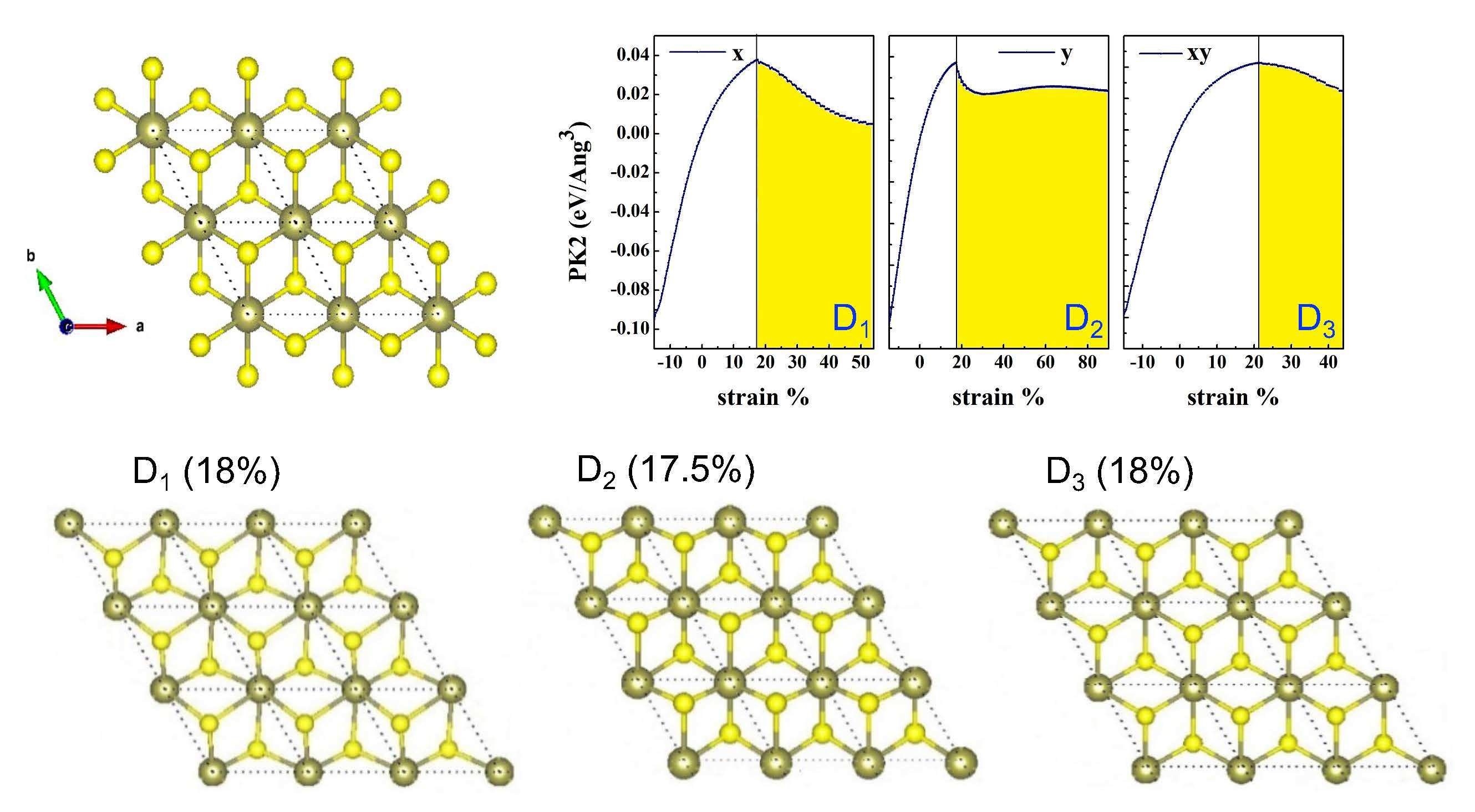
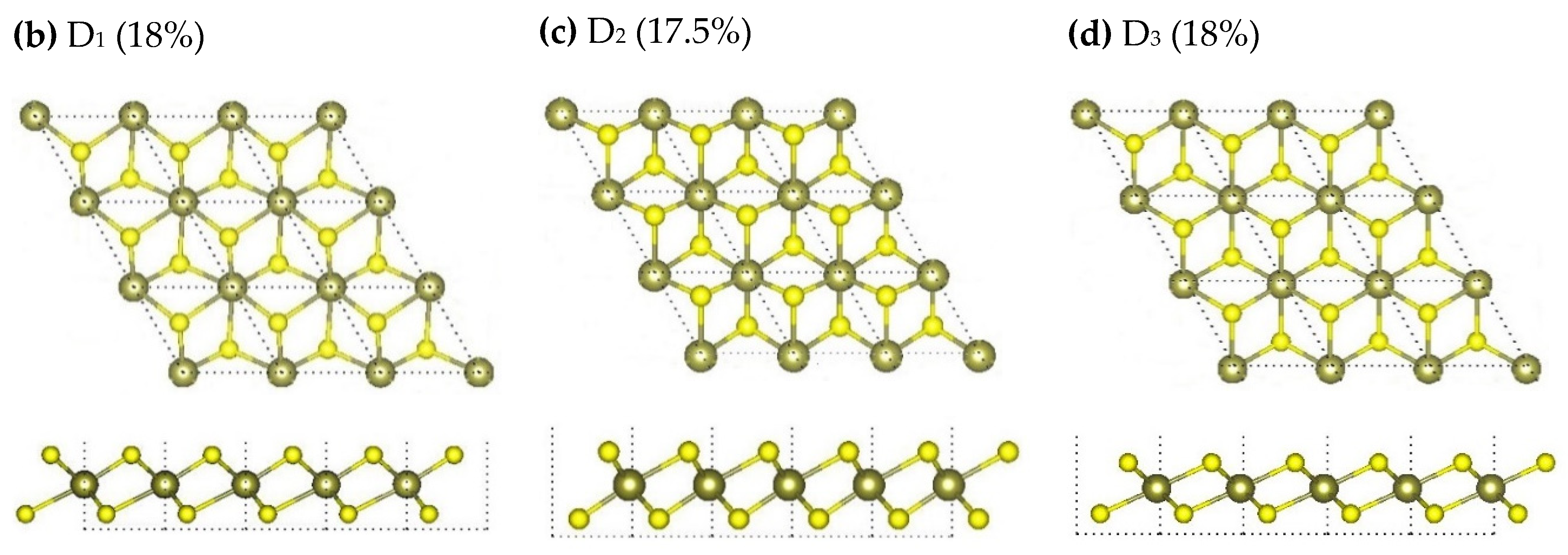
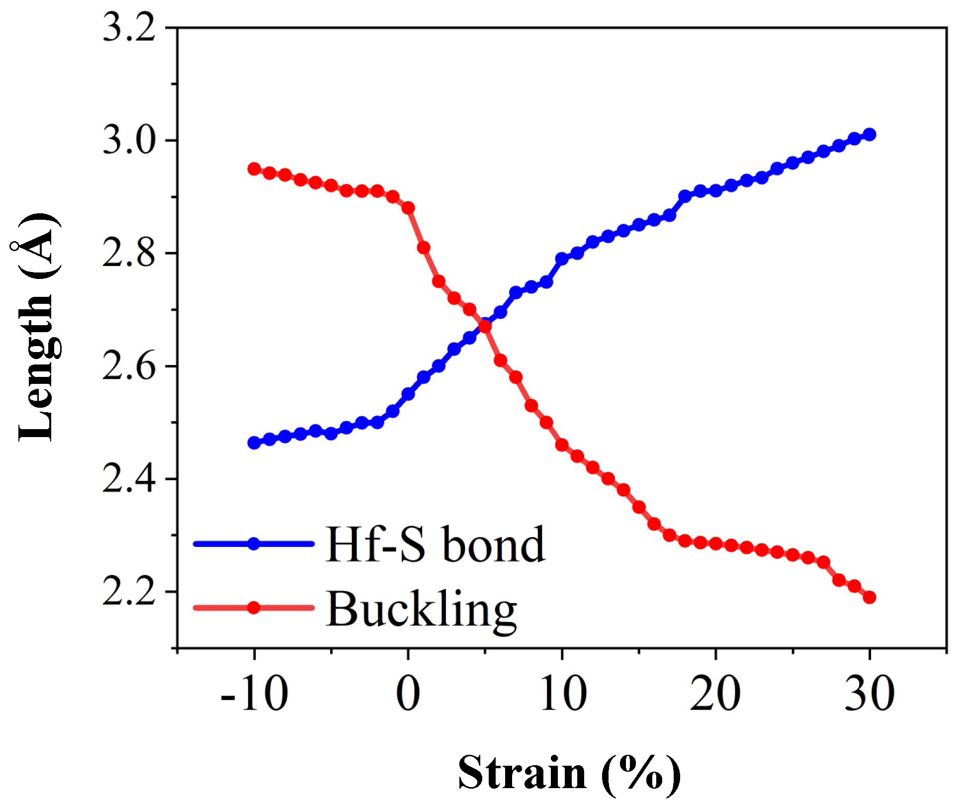
3.1. Atomic Structure

HfS2 monolayer is in a hexagonal phase with an inversion center at the Hf atom sites. Each Hf atom is bounded to six S atoms. The unit cell consists of one Hf atom, and two S atoms. The geometric structure of a HfS2 monolayer is depicted in Figure 1. The obtained optimized lattice constant of HfS2 is 3.64 Å, which is in good agreement with the lattice constant of bulk HfS2, which is reported as 3.63 Å using PBE based calculations [38], and 3.61 Å utilizing vdW-TS/HI method [39]. As can be seen in Table 1, the optimized lattice constant of HfS2 is in a geed agreement with reported lattice constant of similar 2D materials including HfSe2, ZrS2, ZrSe2, GaS, GaSe, and InSe in the literature. The bond length between Hf and S atoms is also calculated as 2.55Å (Figure 1b). This value is in good agreement with reported data in the literature (2.59 Å) [40]. The bond angle between Hf and S atoms (atoms No. 1, 2, and 3) is 88.80°.

3.2. Mechanical Properties

The energy-strain curves for HfS2 monolayer under three types of deformations, namely uniaxial strain along x (D1), y (D2) and biaxial strain along x-y (D3), is analyzed and demonstrated in Figure 2. It is evident that E s differs from the applied strain along with x and y directions. For the tensile and compressive strains through all three modes, E s becomes asymmetric. The strained energy is a quadratic function of strain in the range between 3 % η 5 % for the uniaxial strain along x direction. For the uniaxial strain along y direction and biaxial strain, these harmonic region ranges between 7 % η 3 % and 2 % η 2 % , respectively.
In all three deformation modes, the total energy of the system increases with increasing the applying strain. As can be seen in Figure 2, The changes of Es with strain for D1 and D2 deformation modes is almost the same. However, for D3 deformation mode, the rate of energy change with strain is much higher (Figure 2).

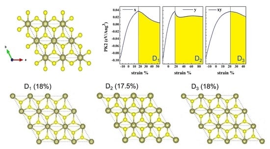
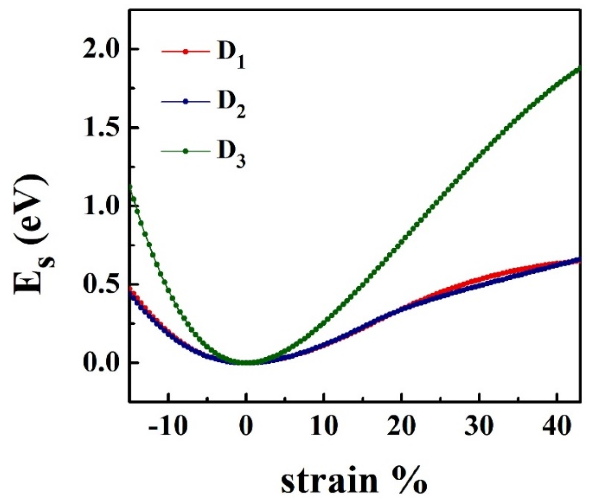
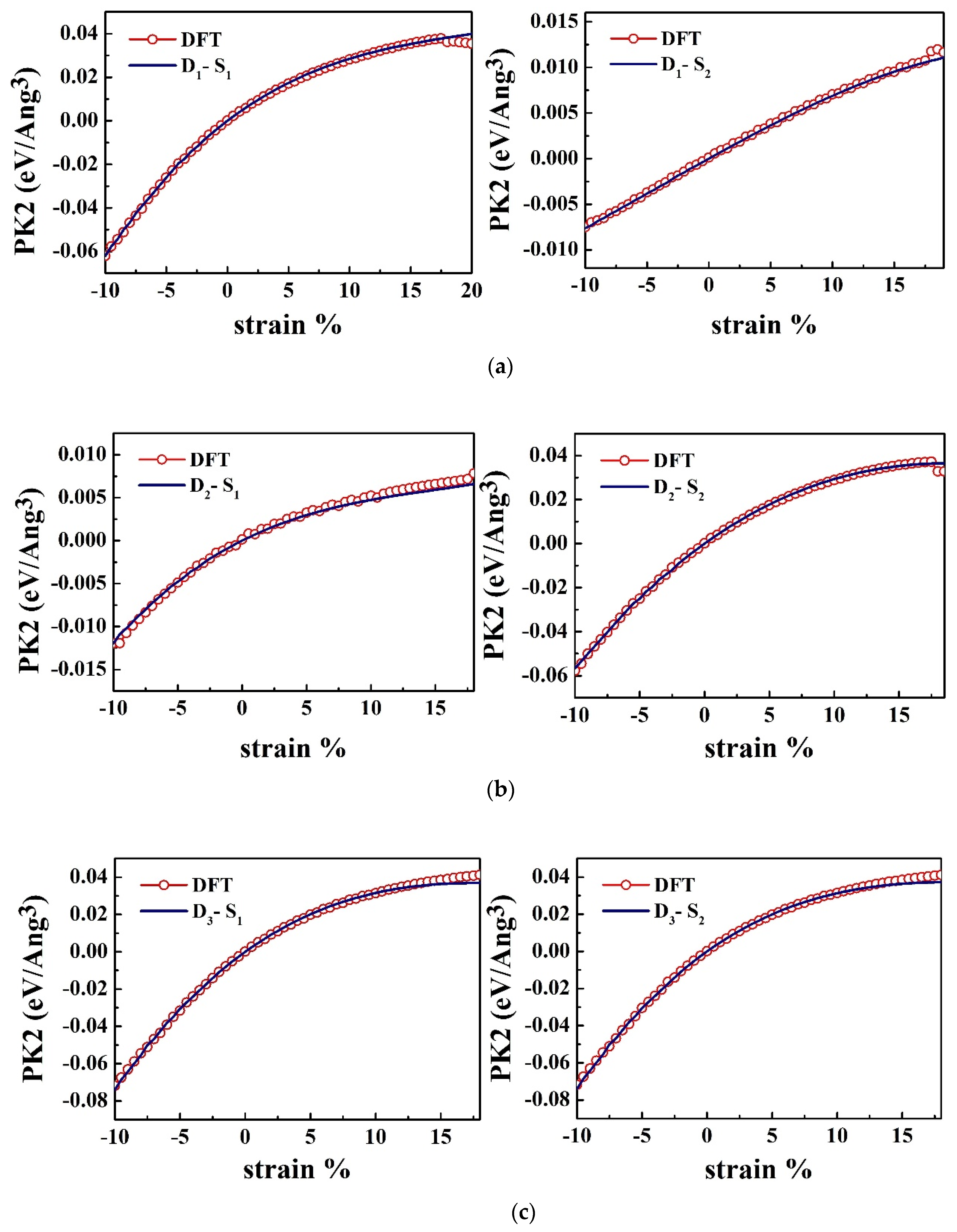
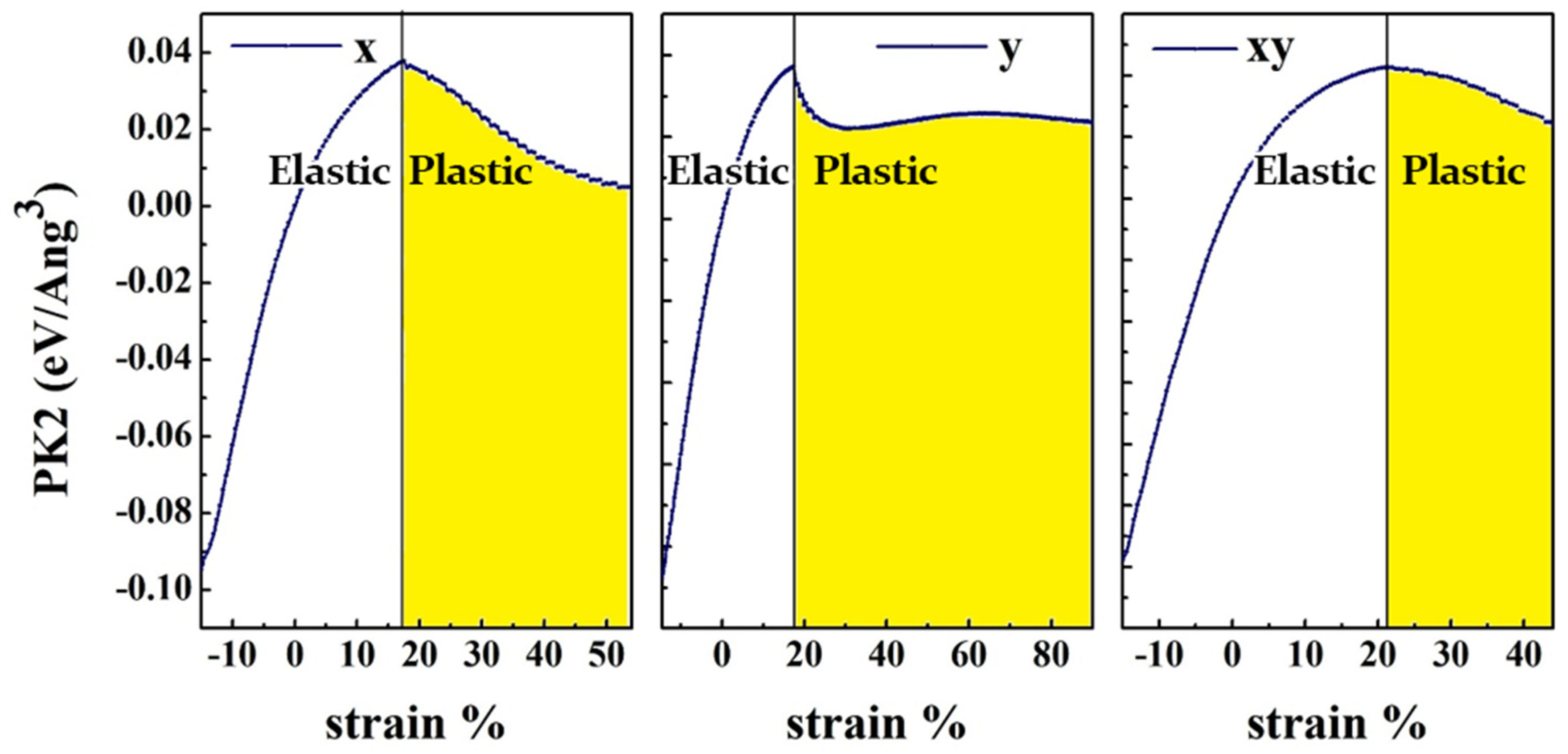
3.3. Strain-Stress Relationship

Figure 3 shows the strain-stress relations obtained from the DFT calculations as well as the fits to these by the equations of continuum theory of elasticity. As can be seen in this figure, the stress-strain curves are depicted for all D1, D2, and D3 deformation modes.
The maximum value in the stress-strain curves shows the ultimate tensile strength (Σm) of the material, in which a material can suffer the maximum respective ηm without damaging (Figure 4). The ultimate strain reflects the intrinsic bonding strengths and acts as a lower limit of the critical strain. Additionally, the values obtained for the ultimate stress and ultimate strain is given in Table 2. Beyond the ultimate strain, the materials will get in a metastable state, which ends up with fracture [42]. The DFT results for strains below the ultimate strain are used to determine the higher-order elastic constants.
As can be seen in Figure 4, the stress increases linearly with increasing strain, within the harmonic (elastic) region. Under larger strains, for the prediction of strain-stress curves, the system is in the anharmonic region in which higher-order terms must be perceived as well. As mentioned previously, the system transits from elastic to the plastic region, when exposed to higher strains. Eventually, Table 3 prepares the nonzero second-, third- and fourth- order elastic constants (SOEC, TOEC and FOEC, respectively) for the HfS2 monolayer.
To comprehensively understand the magnitudes of elastic constants obtained in this work for HfS2, Table 4 presents multiple comparisons between our findings and the other reported elastic constants for similar structures. Furthermore, 2D Young’s moduli (in-plane stiffness) along x and y directions ( Y x 2 D , Y y 2 D ), Poisson’s ratio along x and y directions ( v x 2 D , v y 2 D ), 2D shear modulus (G2D), and the 2D bulk modulus (K), are tabulated in Table 5 and validated by those reported for other structurally similar compounds in the literature.

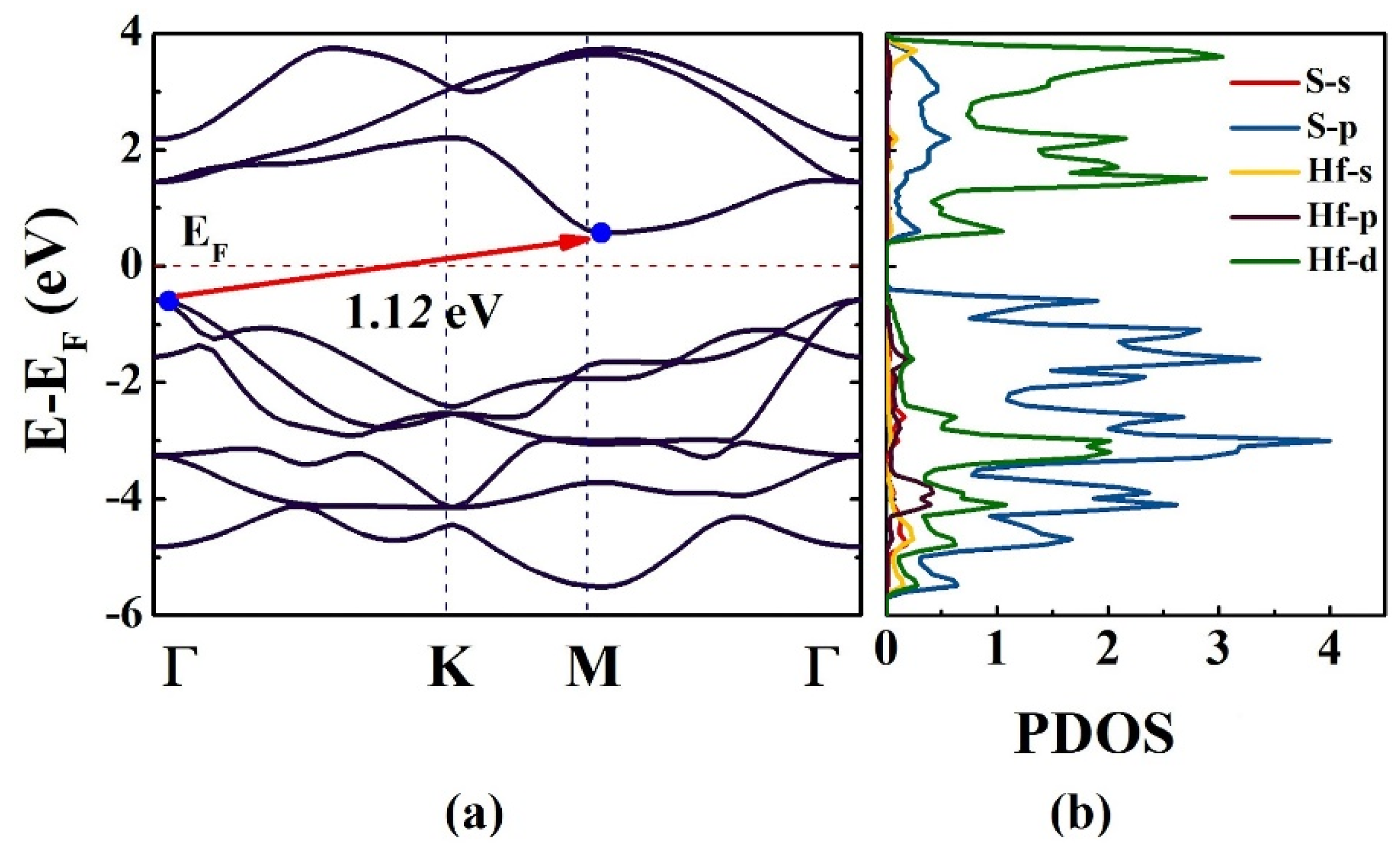
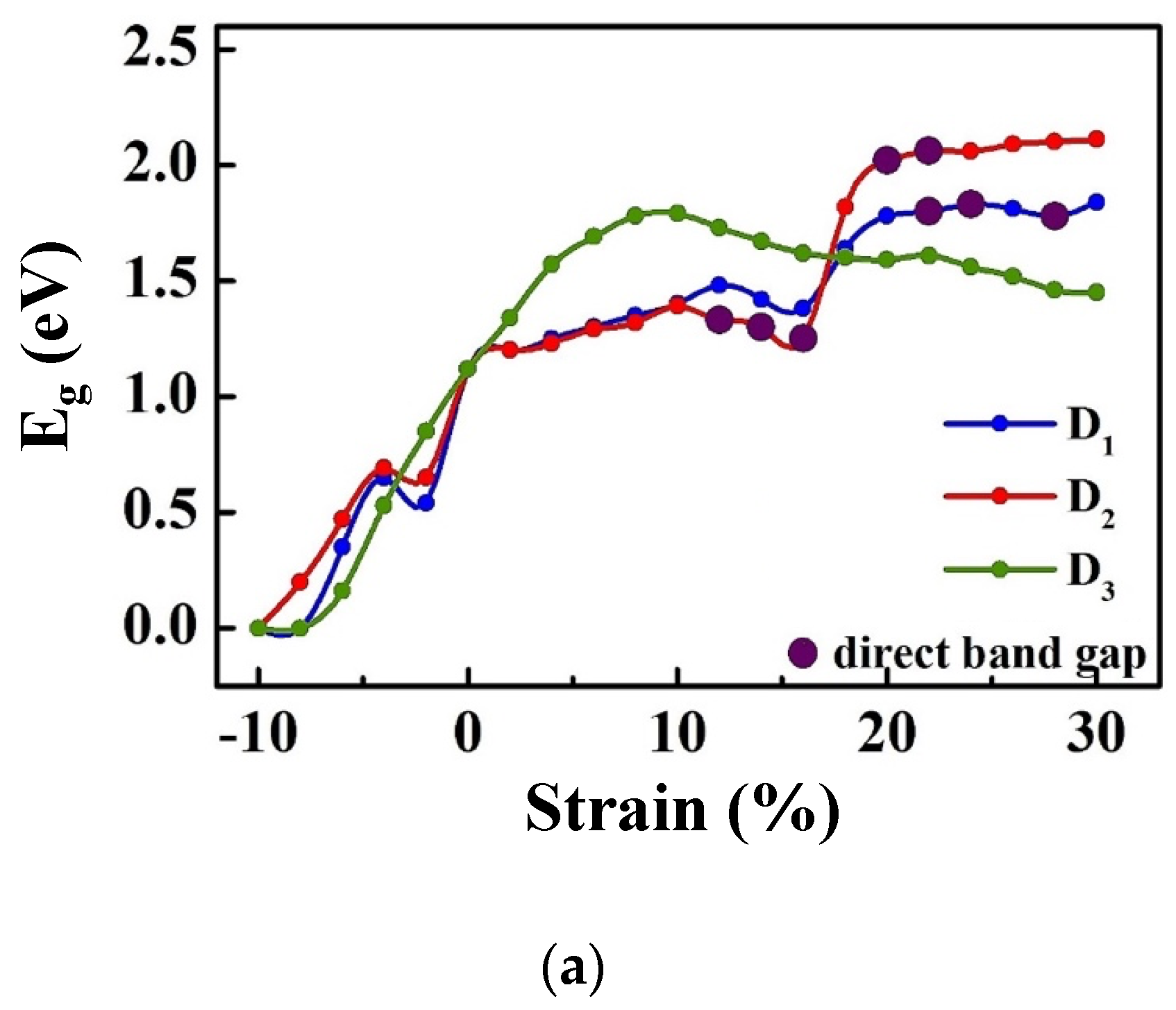
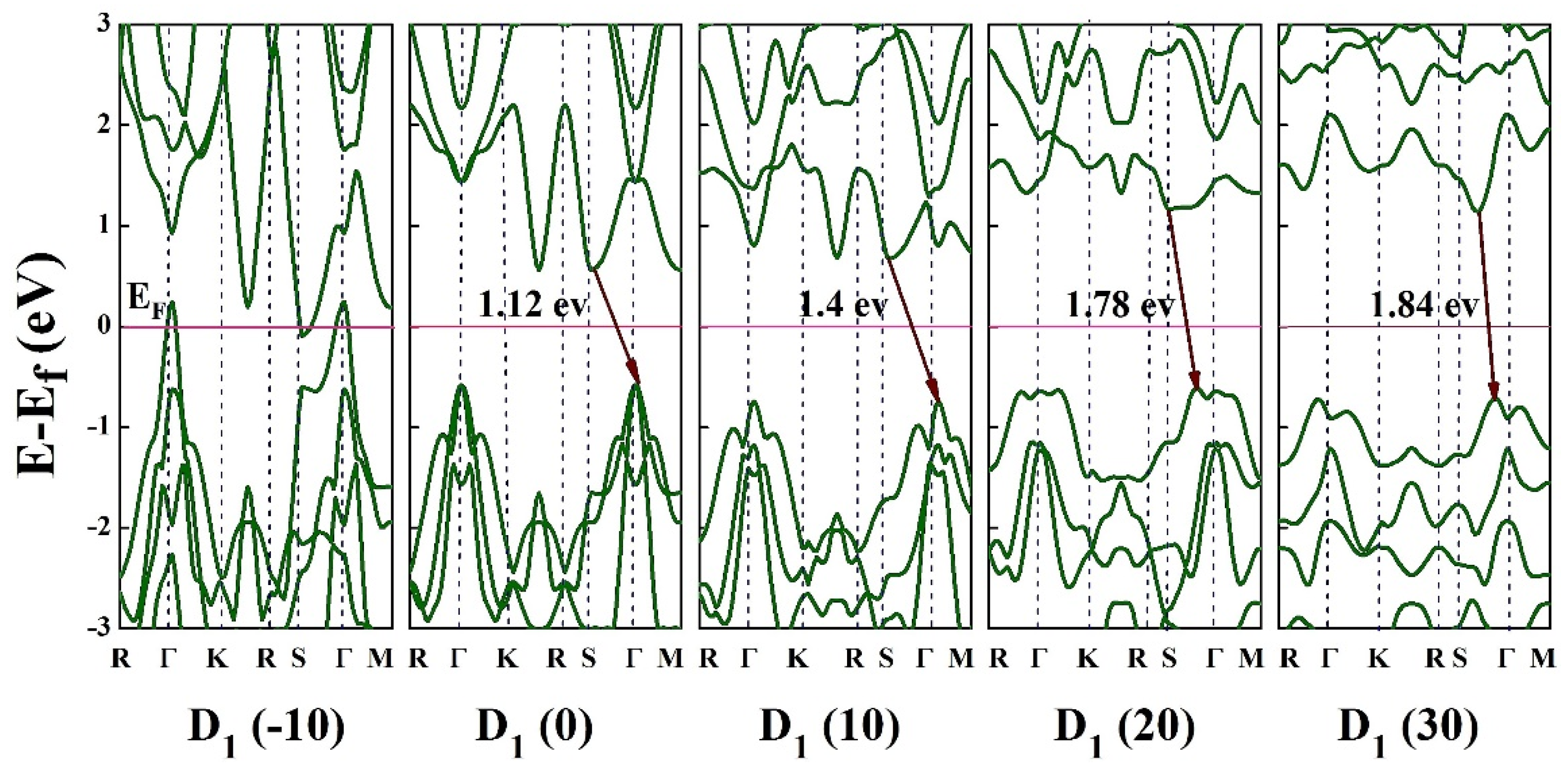
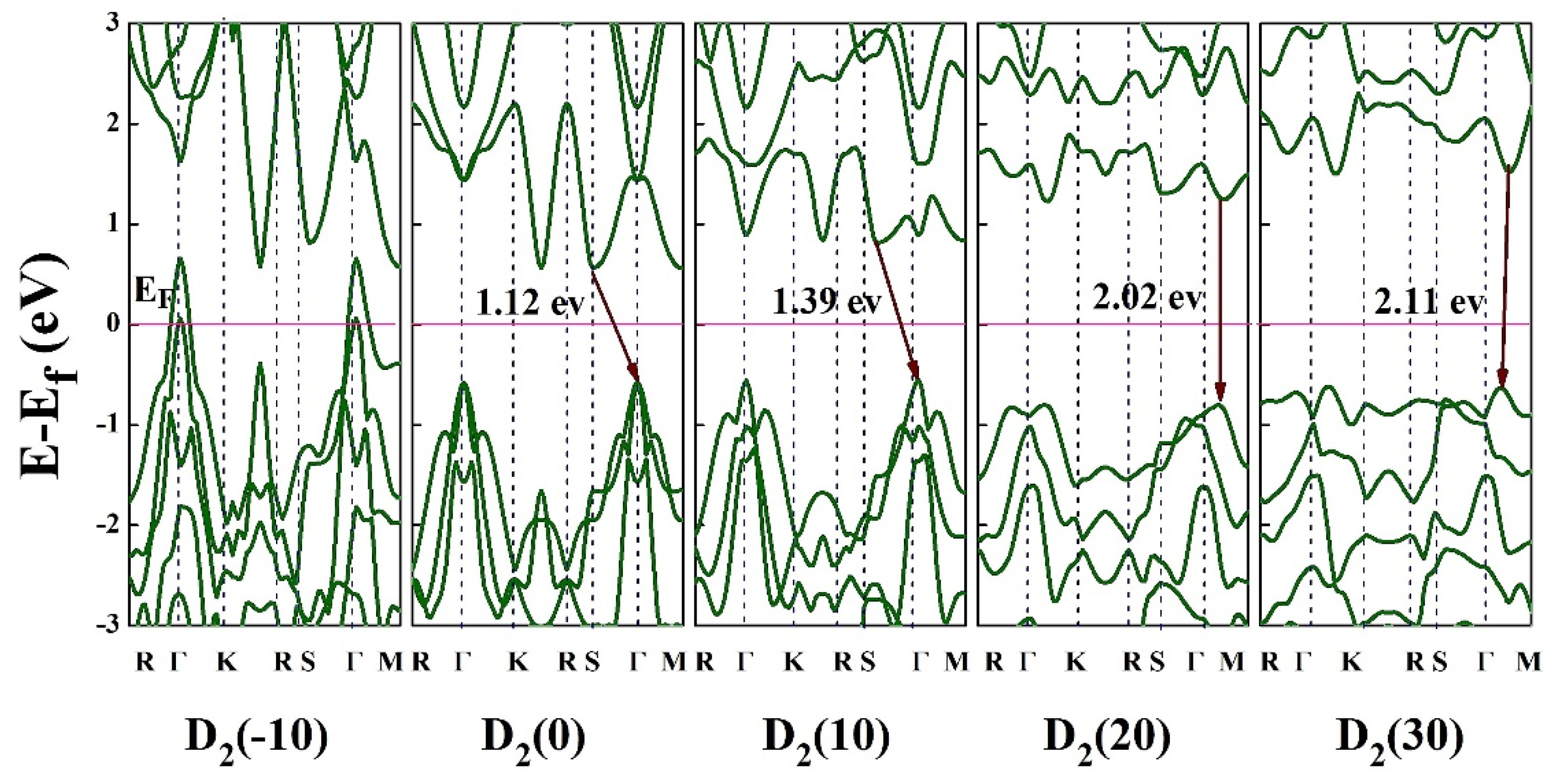
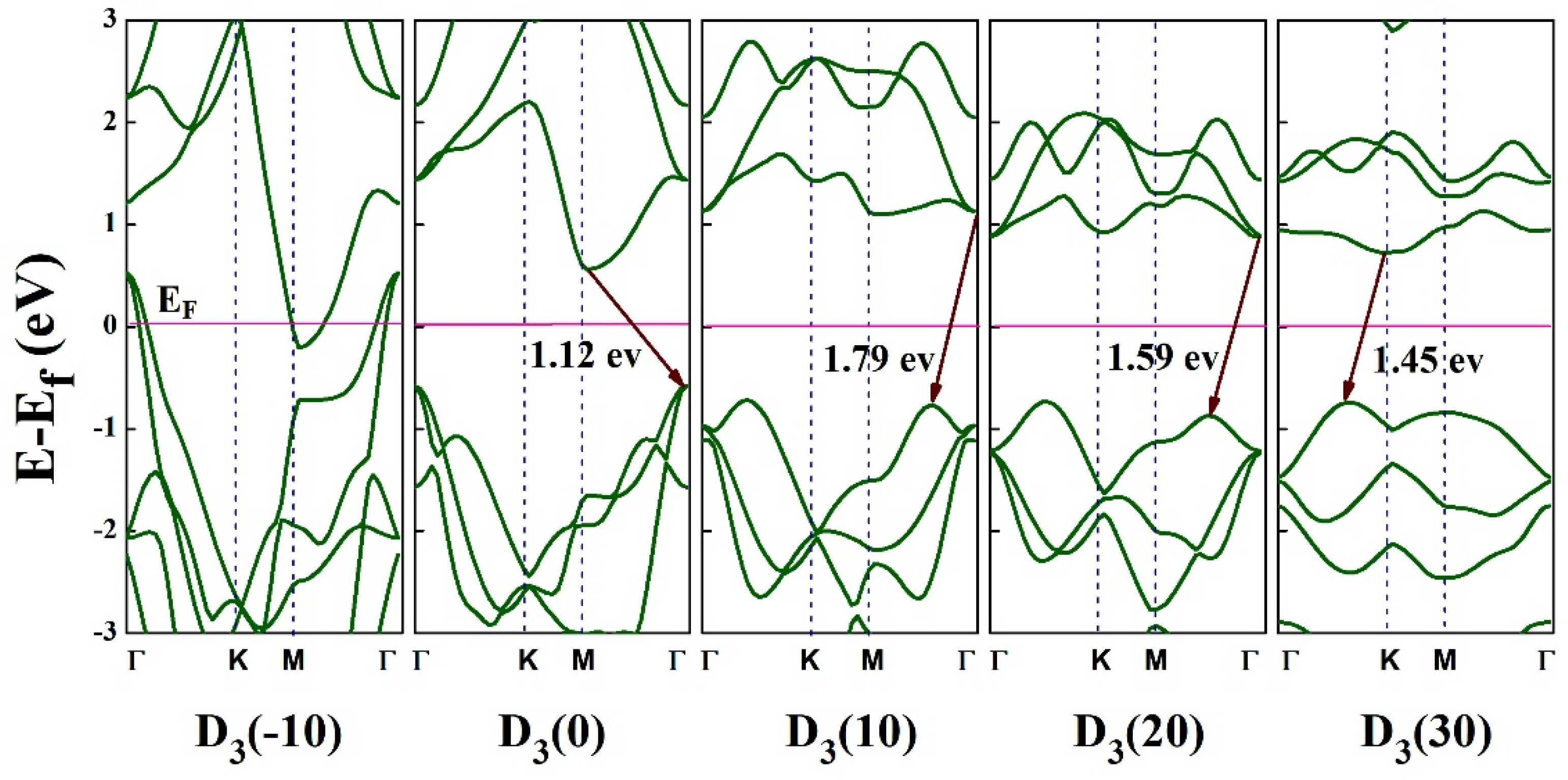
3.4. Electronic Properties

First, we studied the electronic properties of HfS2 in the absence of strain. Figure 5 shows the band structure of the strained structure of HfS2, which is obtained from PBEsol calculations. As can be seen in Figure 5, HfS2 is a semiconductor with an indirect bandgap of 1.12 eV. This value is compared with other methods of HfS2 ( E g L D A = 1.07 eV [40], E g G G A = 1.15 eV [43], E g HSE 06 = 2.02 eV [44], and E g G W = 2.45 eV [45]), where it is in a good agreement with E g G G A = 1.15 eV [43]. As can be seen in Table 4, The predicted gap energies by GW and HSE06 are larger than the predicted gap energy by PBE approximation. Since the HSE06 functional can accurately predict enthalpies of formation, ionization potentials, and electron affinities for lattice constants and band gaps of solids in general, the predicted gap energy by HSE06 is larger and more accurate than the predicted gap energy by PBE [46]. Also, in GW calculations, the excitonic effects are included and due to the fact that the excitonic effects are significant in 2D semiconductors, the predicted gap energy by GW is twice larger than the predicted gap energy by GGA approximation for the HfS2 monolayer (Table 4) [47].
In our predicted electronic structure (Figure 5), it can be seen that the conduction-band minimum (CBM) and valence-band maximum (VBM) are located at M and Γ points, respectively. Additionally, we examine the projected density of states (PDOS), which demonstrates the contribution of orbitals in the valence and conduction bands of the material. In the conduction band, Hf-5d orbitals have the maximum contribution. In contrast, the 3p orbital of S atom makes a greater contribution in the valance band near the Fermi level, as shown in Figure 5b.
In the next step, we investigated the electronic behavior of HfS2 under different strains. The bandgap variation of HfS2 monolayer under these three types of strain are shown in Figure 6a. as can be seen in this figure, for all deformation modes, the bandgap decreases when the compressive strain increases 0% to 10%, while it increases when the tensile strain increases from 0% to 10%. In this strain range, we note that the rate of the gap energy decrease/increase with strain is almost the same for D1 and D2 deformation modes. From 10% to 16% tensile strain, the energy gap decreases for all deformation modes. For the strain range from 16% to 20%, the energy gap increases by increasing strain for D1 and D2 deformations, while it keeps decreasing for D3. For the tensile strain ranging from 20% to 30%, the gap energy is almost constant with strain for D1 and D2, while it keeps decreasing for D3. At 22%, 24%, 28% strains along x direction (D1), and at 12%, 14%, 16%, 20%, 22% strains along y direction (D2), the bandgap becomes direct. Under biaxial strain (D3), the semiconducting monolayer maintains its indirect nature, while its energy gap increases with increasing strain and reaches it maximum value (1.79 eV) at 10% strain. For the uniaxial strain in both D1 and D2 cases, when the compressive strain increases from zero to 2%, the energy gap decreases and then gradually increases by increasing the amount of the compressive strain from 2% to 5%. Then, by increasing the strain from 5% to 10%, the energy gap reduces again. For D3 case, the energy gap decreases by increasing the compressive strain from 0 to 10% deformation. As can be seen in Figure 6a, the material becomes metal (Eg = 0 eV) at 10% compressive strain in all three deformation modes. The value of energy gap is the same (1.6 eV) for D1 and D3 at 18% strain, and for D2 at 17.5% strain. As can be observed in Figure 4, at 18% D1 and 17.5% D2 types of deformation, the material is in plastic region, while at 18% D3 type deformation, the material shows elastic deformation (Figure 6b,c,d). As can be seen in Figure 6d, the elastic to plastic transition for D3 occurs at 22% strain.
Our findings indicate that the electronic properties of HfS2 can be effectively tuned by applying planar forces to HfS2 in different directions. Figure 7 shows the band structures of the HfS2 monolayer under uniaxial compressive and tensile strains along the x direction (D1) within the range of −10% to 30%. As can be seen in Figure 7, when the strain ranges from −10% to −8%, bands of energies cross the Fermi level so that HfS2 at these strains under D1 deformation shows a metallic behavior. By reducing the value of strain to −6%, the HfS2 monolayer becomes an indirect semiconductor with a bandgap of 0.35 eV. At the strains above 22%, the bandgap becomes direct and energy of bandgap increases up to 1.8 eV for the D1 case.
In Figure 7, the conduction-band minimum (CBM) is located at S point, while the valence-band maximum (VBM) is located at the Γ point, which is shifted to the S point by increasing the strain. These points indicate the transformation of bandgap from indirect to direct with strain engineering.
For the deformed HfS2 under the tensile strain along y direction (D2), by increasing the strains from 0% to 30%, the bandgap increases from 1.12 eV to its maximum value of 2.11 eV continuously. The band structure of strain HfS2 monolayer under uniaxial compressive and tensile strain along y direction (D2) is shown in Figure 8. Under the compressive strain of D2 deformation, there is no bandgap near the Fermi level so the system is metallic. In addition, it remains as an indirect semiconductor over the entire applied compressive strain domain when it is strained along y direction (D2). However, under tensile straining, at 12% to 22% strains, the gap is direct and energy bandgap changes from 1.33 to 2.06 eV. When the compressive strain is applied (D2), the located CBM at S point moves to Γ point, and the VBM at the Γ point moves to M point. By applying tensile strain, CBM gets away from the Fermi level and the bandgap increases from 1.12 eV (at unstrained condition) to 2.11 eV (strained with 30% tensile strain).
In Figure 9 the band structure of strained HfS2 monolayer under biaxial strain along x-y (D3) ranging from −10% to 30% strain is shown. As can be seen in Figure 9, under compressive strain ranging from −10% to −6% strains, the bands cross the Fermi level and the system shows metallic behavior. At −6% strain and beyond (−6 < strain < 0), the HfS2 monolayer becomes an indirect semiconductor with a bandgap of 0.16 eV in −6% strain. In the tensile deformation domain, the gap energy increases increasing the stain. At 0%, 10%, 20%, and 30% strains, the bandgap becomes 1.12 eV, 1.79 eV, 1.59 eV and 1.45 eV, respectively. The CBM is located at M, Г, Г and K point for 0%, 10%, 20%, and 30% strain, respectively. Also, the VBM at 0%, 10%, 20% strains are located between M and Г points and at 30% strain, it is located between Г and K points.
Graphene has a plate structure and its symmetry is not broken during deformation. Therefore, not only graphene does not suffer any bulking during deformation, but also only monotonic changes can occur on its electron properties during the biaxial straining (Figure 10) [48]. While, the HfS2 structure is not a plate like structure, its electronic properties are affected by the occurred buckling during the deformation. It is expected to observe many changes in the symmetry of the structure and the distance and angle of the atoms in the strained HfS2 monolayers. Such structural changes can greatly affect the electronic properties and therefore, the bandgap changes of HFS2 will not be monotonic under biaxial strains (Figure 6).

4. Conclusions

In summary, the mechanical and electronic properties of the HfS2 monolayer under two uniaxial (D1 and D2) and one biaxial (D3) DFT calculations is investigated. We determined the harmonic regions in the different deformation modes. This harmonic region ranges in 3 % η 5 % , 7 % η 3 % and 2 % η 2 % for D1, D2, and D3, respectively. Our findings reveal that the ultimate stress of the HfS2 monolayer for D1, D2, and D3 is 0.037   e V Å 3   , 0.038   e V Å 3 ,and 0.044   e V Å 3 , respectively. The obtained ultimate strain is 17%, 17.5% and 21% strain for D1, D2, and D3 respectively. The high order of elastic constants including second-, third-, and fourth-order constants are calculated. The values of 2D Young’s moduli along x and y directions are predicted as 83.01 N/m and 83.57 N/m, respectively. The value of Poisson’s ratio along x and y directions is the same (0.17) for both D1 and D2.
Moreover, the electronic properties of HfS2 show that it is a semiconductor with an indirect bandgap of 1.12 eV. The projected density of states (PDOS) indicates the conduction band, Hf-5d orbital possesses the maximum contribution, while the 3p orbital of S atom have greatest contribution in the valance band. The variation of band structure and bandgap of the HfS2 monolayer under D1, D2, and D3 deformation modes in the range of −10% to 30% are also investigated. We tuned the bandgap state (direct vs. indirect), gap energy (opening vs. shrinking), and phase transition (semiconductor- metal) by strain engineering under different deformation modes. Our findings reveal how to utilize strain engineering to make HfS2 monolayer as a suitable candidate for a wide range of applications including flexible solar cells, electronics and optoelectronics.

Author Contributions

DFT calculations: M.F., S.A.G., S.G.S., and A.A.; validation: M.F., and A.A.; analysis M.F., and A.A.; writing—original draft preparation: M.F., and A.A.; writing—review and editing: A.R.; and supervision: A.R. All authors have read and agreed to the published version of the manuscript.

Funding

This research received no external funding.

Conflicts of Interest

The authors declare no competing financial interest.

References

  1. Kang, J.; Tongay, S.; Zhou, J.; Li, J.; Wu, J. Band offsets and heterostructures of two-dimensional semiconductors. Appl. Phys. Lett. 2013, 102, 012111. [Google Scholar] [CrossRef] [Green Version]
  2. Neto, A.; Novoselov, K. Two-dimensional crystals: Beyond graphene. Mater. Express 2011, 1, 10–17. [Google Scholar] [CrossRef]
  3. Gui, G.; Li, J.; Zhong, J. Band structure engineering of graphene by strain: First-principles calculations. Phys. Rev. B 2008, 78, 075435. [Google Scholar] [CrossRef] [Green Version]
  4. Chhowalla, M.; Shin, H.S.; Eda, G.; Li, L.-J.; Loh, K.P.; Zhang, H. The chemistry of two-dimensional layered transition metal dichalcogenide nanosheets. Nat. Chem. 2013, 5, 263. [Google Scholar] [CrossRef]
  5. Ansari, R.; Malakpour, S.; Faghihnasiri, M.; Ajori, S. Structural and elastic properties of carbon nanotubes containing Fe atoms using first principles. Superlattices Microstruct. 2013, 64, 220–226. [Google Scholar] [CrossRef]
  6. Butler, S.Z.; Hollen, S.M.; Cao, L.; Cui, Y.; Gupta, J.A.; Gutiérrez, H.R.; Heinz, T.F.; Hong, S.S.; Huang, J.; Ismach, A.F.; et al. Progress, challenges, and opportunities in two-dimensional materials beyond graphene. ACS Nano 2013, 7, 2898–2926. [Google Scholar] [CrossRef]
  7. Xu, K.; Wang, Z.; Wang, F.; Huang, Y.; Wang, F.; Yin, L.; Jiang, C.; He, J. Ultrasensitive Phototransistors Based on Few-Layered HfS2. Adv. Mater. 2015, 27, 7881–7887. [Google Scholar] [CrossRef]
  8. Ahmadi, A.; Faghihnasiri, M.; Shiraz, H.G.; Sabeti, M. Mechanical properties of graphene and its analogous decorated with Na and Pt. Superlattice Microstruct. 2017, 101, 602–608. [Google Scholar] [CrossRef]
  9. Faghihnasiri, M.; Jafari, H.; Ramazani, A.; Shabani, M.; Estalaki, S.M.; Larson, R.G. Nonlinear elastic behavior and anisotropic electronic properties of two-dimensional borophene. J. Appl. Phys. 2019, 125, 145107. [Google Scholar] [CrossRef]
  10. Wang, Q.H.; Kalantar-Zadeh, K.; Kis, A.; Coleman, J.N.; Strano, M.S. Electronics and optoelectronics of two-dimensional transition metal dichalcogenides. Nat. Nanotechnol. 2012, 7, 699. [Google Scholar] [CrossRef]
  11. Abderrahmane, A.; Ko, P.; Thu, T.; Ishizawa, S.; Takamura, T.; Sandhu, A. High photosensitivity few-layered MoSe2 back-gated field-effect phototransistors. Nanotechnology 2014, 25, 365202. [Google Scholar] [CrossRef] [PubMed]
  12. Liu, W.; Kang, J.; Sarkar, D.; Khatami, Y.; Jena, D.; Banerjee, K. Role of metal contacts in designing high-performance monolayer n-type WSe2 field effect transistors. Nano Lett. 2013, 13, 1983–1990. [Google Scholar] [CrossRef] [PubMed]
  13. Gomez, L.; Aberg, I.; Hoyt, J. Electron transport in strained-silicon directly on insulator ultrathin-body n-MOSFETs with body thickness ranging from 2 to 25 nm. IEEE Electron Device Lett. 2007, 28, 285–287. [Google Scholar] [CrossRef]
  14. Derived, C. Ultrasmooth Graphene Nanoribbon Semiconductors. Science 2008, 319, 1229–1232. [Google Scholar]
  15. Zhang, W.; Huang, Z.; Zhang, W.; Li, Y. Two-dimensional semiconductors with possible high room temperature mobility. Nano Res. 2014, 7, 1731–1737. [Google Scholar] [CrossRef] [Green Version]
  16. Zhao, X.; Wang, T.; Wang, G.; Dai, X.; Xia, C.; Yang, L. Electronic and magnetic properties of 1T-HfS2 by doping transition-metal atoms. Appl. Surf. Sci. 2016, 383, 151–158. [Google Scholar] [CrossRef]
  17. Ahmadi, A.; Jafari, H.; Rajipour, M.; Fattahi, R.; Faghihnasiri, M. Nonlinear electronic transport behavior of γ-graphyne nanotubes. IEEE Trans. Electron Devices 2019, 66, 1584–1590. [Google Scholar] [CrossRef]
  18. Novoselov, K.S.; Jiang, D.; Schedin, F.; Booth, T.J.; Khotkevich, V.V.; Morozov, S.V.; Geim, A.K. Two-dimensional atomic crystals. Proc. Natl. Acad. Sci. USA 2005, 102, 10451–10453. [Google Scholar] [CrossRef] [Green Version]
  19. Novoselov, K.S.; Geim, A.K.; Morozov, S.V.; Jiang, D.; Zhang, Y.; Dubonos, S.V.; Grigorieva, I.V.; Firsov, A.A. Electric field effect in atomically thin carbon films. Science 2004, 306, 666–669. [Google Scholar] [CrossRef] [Green Version]
  20. Krowne, C.M. Introduction to examination of 2D hexagonal band structure from a nanoscale perspective for use in electronic transport devices. Adv. Imag. Elect. Phys. 2019, 210, 1. [Google Scholar]
  21. Krowne, C.M. Graphyne and Borophene as Nanoscopic Materials for Electronics. arXiv 2019, arXiv:1912.10876. [Google Scholar]
  22. Schwierz, F. Graphene transistors. Nat. Nanotechnol. 2010, 5, 487. [Google Scholar] [CrossRef] [PubMed]
  23. Hu, P.; Wen, Z.; Wang, L.; Tan, P.; Xiao, K. Synthesis of few-layer GaSe nanosheets for high performance photodetectors. ACS Nano 2012, 6, 5988–5994. [Google Scholar] [CrossRef] [PubMed]
  24. Radisavljevic, B.; Radenovic, A.; Brivio, J.; Giacometti, I.V.; Kis, A. Single-layer MoS2 transistors. Nat. Nanotechnol. 2011, 6, 147. [Google Scholar] [CrossRef] [PubMed]
  25. Chen, H.; Müller, M.B.; Gilmore, K.J.; Wallace, G.G.; Li, D. Mechanically strong, electrically conductive, and biocompatible graphene paper. Adv. Mater. 2008, 20, 3557–3561. [Google Scholar] [CrossRef]
  26. Chen, J. Phonons in bulk and monolayer HfS2 and possibility of phonon-mediated superconductivity: A first-principles study. Solid State Commun. 2016, 237, 14–18. [Google Scholar] [CrossRef]
  27. Kang, J.; Sahin, H.; Peeters, F.M. Mechanical properties of monolayer sulphides: A comparative study between MoS2, HfS2 and TiS3. Phys. Chem. Chem. Phys. 2015, 17, 27742–27749. [Google Scholar] [CrossRef]
  28. Blöchl, P.E. Projector augmented-wave method. Phys. Rev. B 1994, 50, 17953. [Google Scholar] [CrossRef] [Green Version]
  29. Espresso, Q. A modular and open-source software project for quantum simulations of materials/P. J. Phys. Condens. Matter 2009, 21, 395502. [Google Scholar]
  30. Perdew, J.P.; Ruzsinszky, A.; Csonka, G.; Vydrov, O.A.; Scuseria, G.E.; Constantin, L.A.; Zhou, X.; Burke, K. Restoring the density-gradient expansion for exchange in solids and surfaces. Phys. Rev. Lett. 2008, 100, 136406. [Google Scholar] [CrossRef] [Green Version]
  31. Monkhorst, H.J.; Pack, J.D. Special points for Brillouin-zone integrations. Phys. Rev. B 1976, 13, 5188. [Google Scholar] [CrossRef]
  32. Peng, Q.; Ji, W.; De, S. Mechanical properties of the hexagonal boron nitride monolayer: Ab initio study. Comput. Mater. Sci. 2012, 56, 11–17. [Google Scholar] [CrossRef] [Green Version]
  33. Reddy, J.N. An Introduction to the Finite Element Method, 3rd ed.; McGraw Hill: New York, NY, USA, 2006. [Google Scholar]
  34. Hammerand, D.C.; Kapania, R.K. Thermoviscoelastic analysis of composite structures using a triangular flat shell element. AIAA J. 1999, 37, 238–247. [Google Scholar] [CrossRef]
  35. Wei, X.; Fragneaud, B.; Marianetti, C.A.; Kysar, J.W. Nonlinear elastic behavior of graphene: Ab initio calculations to continuum description. Phys. Rev. B 2009, 80, 205407. [Google Scholar] [CrossRef] [Green Version]
  36. Thorpe, M.; Sen, P. Elastic moduli of two-dimensional composite continua with elliptical inclusions. J. Acoust. Soc. Am. 1985, 77, 1674–1680. [Google Scholar] [CrossRef]
  37. Andrew, R.C.; Mapasha, R.E.; Ukpong, A.M.; Chetty, N. Mechanical properties of graphene and boronitrene. Phys. Rev. B 2012, 85, 125428. [Google Scholar] [CrossRef] [Green Version]
  38. Lv, H.; Lu, W.; Luo, X.; Lu, H.; Zhu, X.; Sun, Y. Enhancing the thermoelectric performance of a HfS2 monolayer through valley engineering. arXiv 2016, arXiv:1608.05464. [Google Scholar]
  39. Zhao, Q.; Guo, Y.; Si, K.; Ren, Z.; Bai, J.; Xu, X. Elastic, electronic, and dielectric properties of bulk and monolayer ZrS2, ZrSe2, HfS2, HfSe2 from van der Waals density-functional theory. Phys. Status Solidi 2017, 254, 1700033. [Google Scholar] [CrossRef]
  40. Singh, D.; Gupta, S.K.; Sonvane, Y.; Kumar, A.; Ahuja, R. 2D-HfS2 as an efficient photocatalyst for water splitting. Catal. Sci. Technol. 2016, 6, 6605–6614. [Google Scholar] [CrossRef]
  41. Rasmussen, F.A.; Thygesen, K.S. Computational 2D materials database: Electronic structure of transition-metal dichalcogenides and oxides. J. Phys. Chem. C 2015, 119, 13169–13183. [Google Scholar] [CrossRef]
  42. Topsakal, M.; Cahangirov, S.; Ciraci, S. The response of mechanical and electronic properties of graphane to the elastic strain. Appl. Phys. Lett. 2010, 96, 091912. [Google Scholar] [CrossRef] [Green Version]
  43. Ahuja, R.; Piquini, P.C. HfS2 and TiS2 Monolayers with Adsorbed C, N, P Atoms: A First Principles Study. Catalysts 2020, 10, 2073–4344. [Google Scholar]
  44. Lu, H.; Guo, Y.; Robertson, J. Band edge states, intrinsic defects, and dopants in monolayer HfS2 and SnS2. Appl. Phys. Lett. 2018, 112, 062105. [Google Scholar] [CrossRef] [Green Version]
  45. Zhuang, H.L.; Hennig, R.G. Computational search for single-layer transition-metal dichalcogenide photocatalysts. J. Phys. Chem. C 2013, 117, 20440–20445. [Google Scholar] [CrossRef]
  46. Krukau, A.V.; Vydrov, O.A.; Izmaylov, A.F.; Scuseria, G.E. Influence of the exchange screening parameter on the performance of screened hybrid functionals. J. Chem. Phys. 2006, 125, 224106. [Google Scholar] [CrossRef]
  47. Ugeda, M.M.; Bradley, A.J.; Shi, S.F.; Felipe, H.; Zhang, Y.; Qiu, D.Y.; Ruan, W.; Mo, S.K.; Hussain, Z.; Shen, Z.X.; et al. Crommie. Giant bandgap renormalization and excitonic effects in a monolayer transition metal dichalcogenide semiconductor. Nat. Mater. 2014, 13, 1091–1095. [Google Scholar] [CrossRef] [Green Version]
  48. Katin, K.P.; Krylov, K.S.; Maslov, M.M.; Mur, V.D. Tuning the supercritical effective charge in gapless graphene via Fermi velocity modifying through the mechanical stretching. Diam. Relat. Mater. 2019, 100, 107566. [Google Scholar] [CrossRef]
Figure 1. (a) Top view and (b) side view of the atomic structure of the hexagonal HfS2 monolayer. The light brown and yellow balls represent Hf and S atoms, respectively. The black rectangle denotes the unit cell.
Nanomaterials 10 00446 g001
Figure 2. The energy-strain per atom of HfS2 monolayer under the uniaxial strain along x (D1) and y (D2) directions, and biaxial strain along x-y (D3).
Nanomaterials 10 00446 g002
Figure 3. Strain-stress relationships for three types of strain, namely (a) D1 (b) D2 (c) D3, fitted with S1 and S2, which denote to the x and y components of the stress, respectively.
Nanomaterials 10 00446 g003
Figure 4. Σm and ηm denote the x, y, and x-y components of the stress and strain, respectively. The line separates the harmonic and anharmonic regions. The yellow area shows the plastic region.
Nanomaterials 10 00446 g004
Figure 5. Band structure (a) and PDOS (b) of the HfS2 monolayer in free-strain condition. The Fermi level is set to zero.
Nanomaterials 10 00446 g005
Figure 6. (a) The bandgap variations of the HfS2 monolayer under uniaxial strain along x (D1) and y (D2) directions and the biaxial strains along x-y (D3). (b) The deformed lattice structures of the HfS2 monolayer at uniaxial 18% tensile strain along x direction (D1), (c) the deformed lattice structures of the HfS2 monolayer at under uniaxial strains of 17.5% along y direction, and (d) the deformed lattice structures of the HfS2 monolayer at 18% biaxial strain along x-y directions (D3). The top and side views are shown in the top and bottom panels, respectively.
Nanomaterials 10 00446 g006aNanomaterials 10 00446 g006b
Figure 7. Band structure of HfS2 monolayer under the uniaxial strains in the range of −10% to 30% along x direction. The Fermi level is set to zero.
Nanomaterials 10 00446 g007
Figure 8. Electronic band structure of HfS2 monolayer under the uniaxial strains in the range of −10% to 30% along y direction. The Fermis level is set to zero.
Nanomaterials 10 00446 g008
Figure 9. Band structure of the HfS2 monolayer under D3 deformation in the range of −10% to 30%.
Nanomaterials 10 00446 g009
Figure 10. Hf-S bond length and buckling of the HfS2 monolayer under D3 deformation in the range of −10% to 30% straining.
Nanomaterials 10 00446 g010
Table 1. Comparison of the lattice constants of 2D HfS2 are calculated using different exchange-correlation functions along with the other reported values in the literature.
MaterialMethodLattice Constant
HfS2PBEsol (This work)3.64
GGA [40]3.54
HSE [40]3.53
LDA [40]3.38
PBE (bulk) [41]3.54
PBE (bulk) [38]3.63
vdW-TS/HI [39]3.61
HfSe2vdW-TS/HI [39]3.70
ZrS2vdW-TS/HI [39]3.64
ZrSe2vdW-TS/HI [39]3.74
GaSDFT-PBE [41]3.64
GaSeDFT-PBE [41]3.82
InSeDFT-PBE [41]4.09
Table 2. Ultimate strains (ηm) and ultimate stresses (Σm) for three (D1, D2, and D3) types of strains.
Uniaxial (x)Uniaxial (y)Biaxial (x-y)
Σ m (eV/Å3)
η m
0.037
17.2%
0.038
17.51%
0.044
21.17%
Table 3. Nonzero second-, third- and fourth-order elastic constants (in N/m) for the HfS2 monolayer.
SOECTOECFOEC
C1186.29C111−683.81C11113389.08
C1215.28C112−14.69C1112−343.81
C2285.71C222−561.10C22221092.89
C6668.14C122−145.42C1222968.49
C166−205.85C6666−592.82
C266−1118C12662386.80
C1122−42.83
C2266−2207.16
C1166471.75
Table 4. Elastic constants C11 and C12 obtained in this work along with those reported in a previous works (in units of N/m).
MaterialC11C12
HfS2 (This work)86.2915.28
GaS [41]8318
GaSe [41]7016
InSe [41]5112
h-BN [32]293.266.1
ZrS2 [39]131.4725.63
ZrSe2 [39]104.6221.31
HfS2 [39]141.9825.95
HfSe2 [39]116.8822.30
Ref [39] is in the bulk structure.
Table 5. 2D Young’s moduli, Poisson’s ratio, 2D shear modulus, and 2D bulk modulus for some 2D materials.
Material Y x 2 D   ( N / m ) Y y 2 D   ( N / m ) v x 2 D v y 2 D G 2 D   ( N / m ) K (N/m)
HfS283.0183.570.170.1768.1450.85
ZrS2 [39]57.220.2023.85 (GPa)31.73 (GPa)
ZrSe2 [39]52.330.1922.02 (GPa)27.99 (GPa)
HfSe2 [39]69.590.1929.34 (GPa)36.87 (GPa)
h-BN [32]279.20.2176-160 (GPa)

