Van der Waals Integrated Silicon/Graphene/AlGaN Based Vertical Heterostructured Hot Electron Light Emitting Diodes


Abstract
1. Introduction
2. Materials and Methods
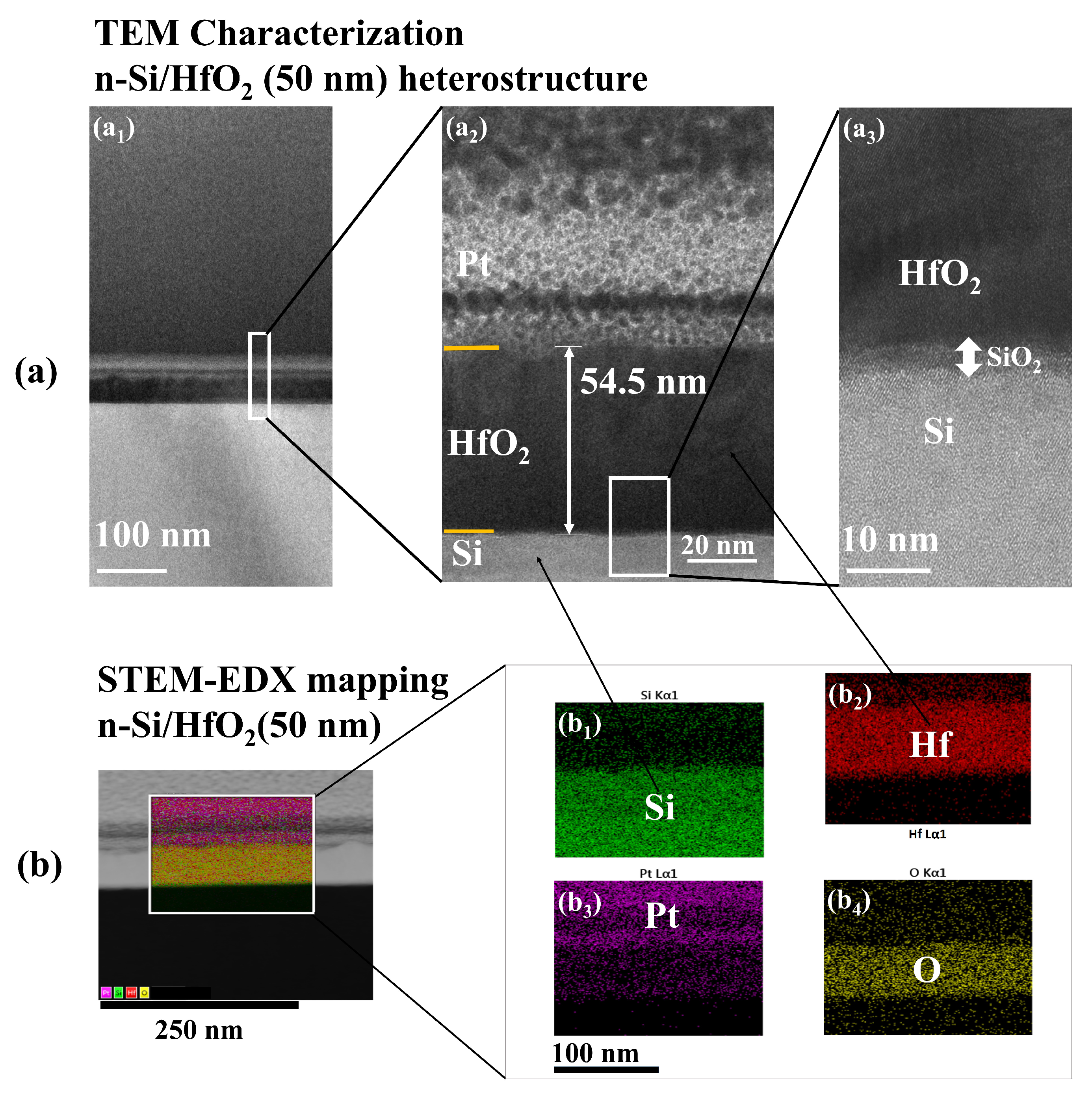
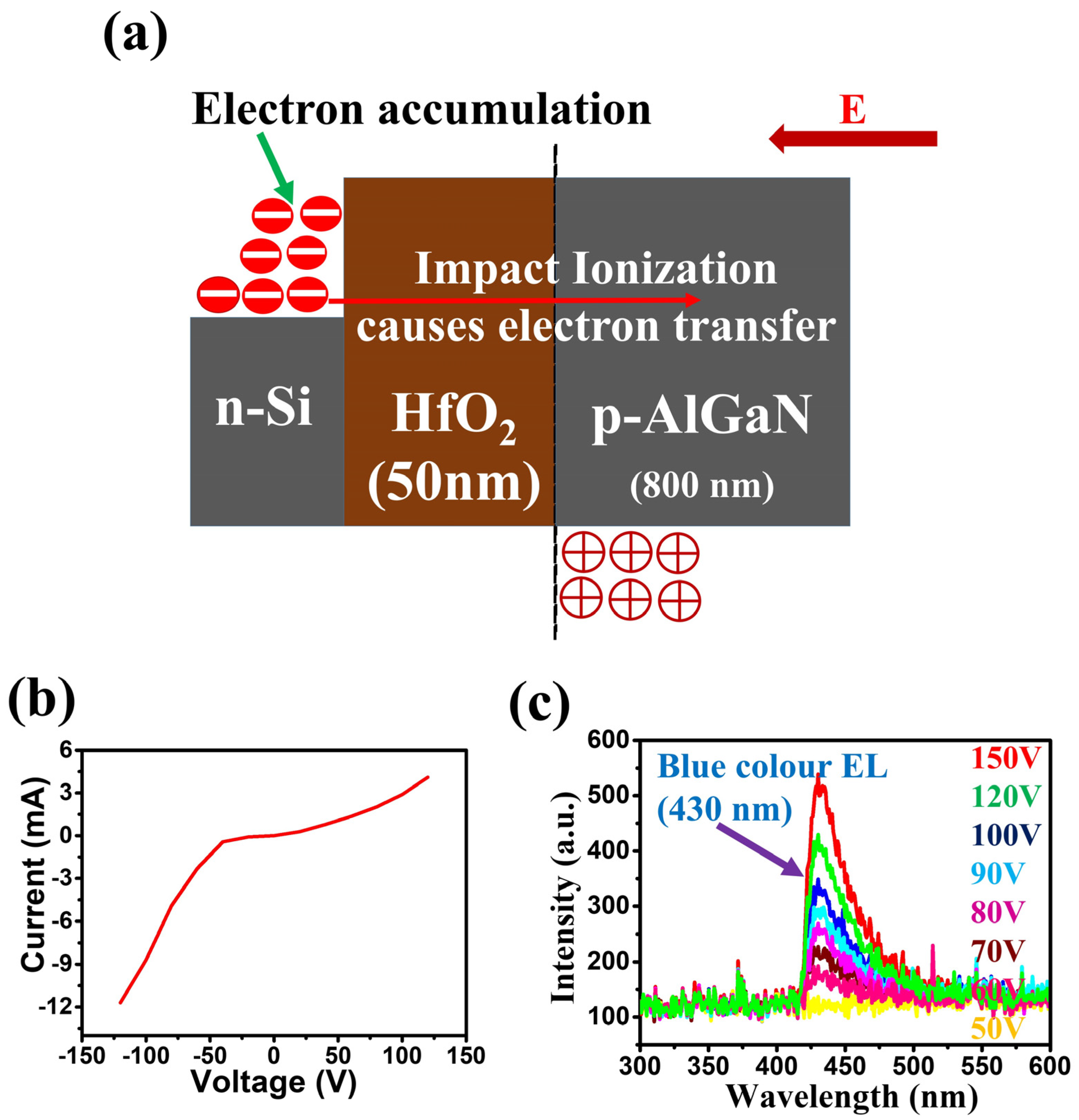
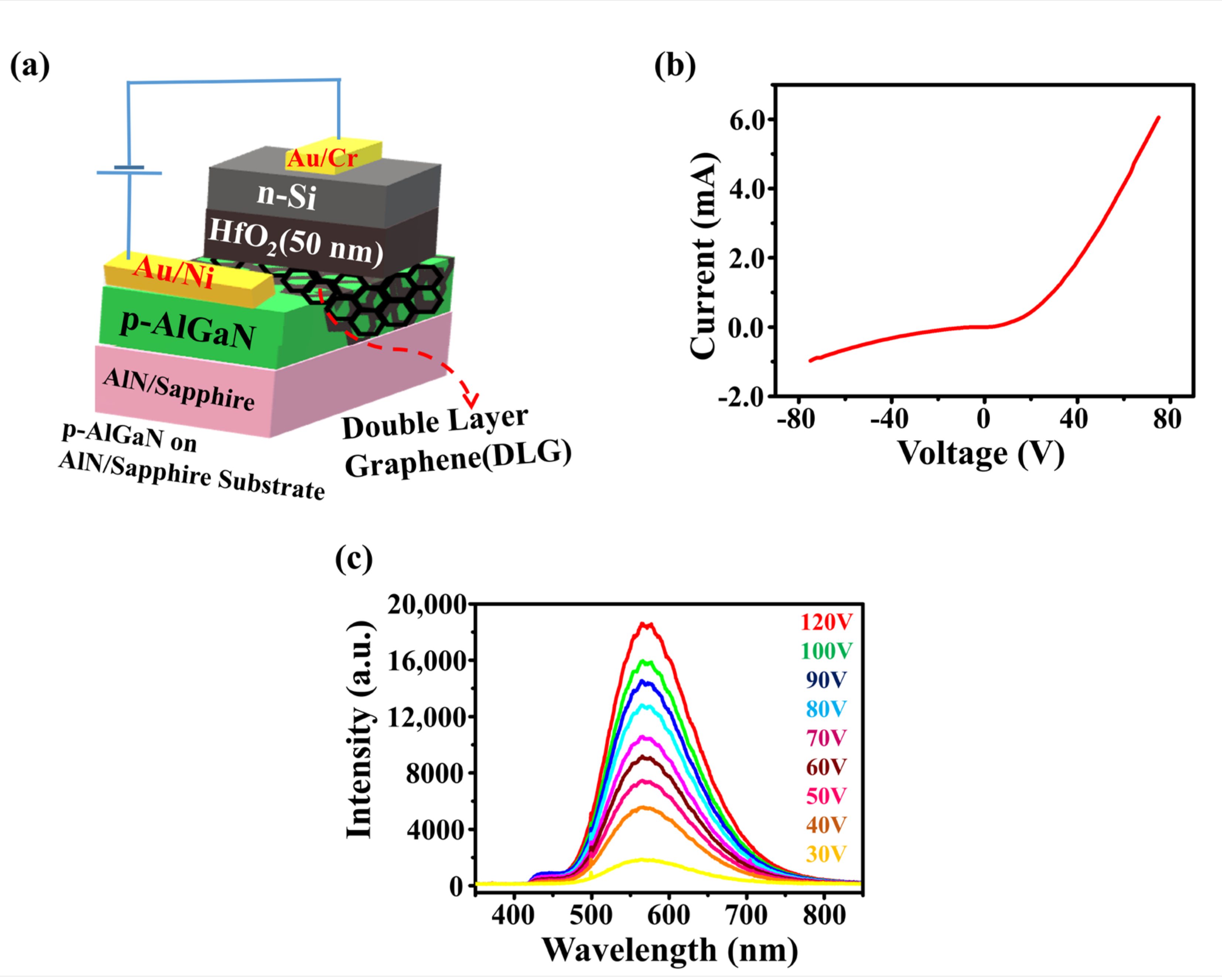
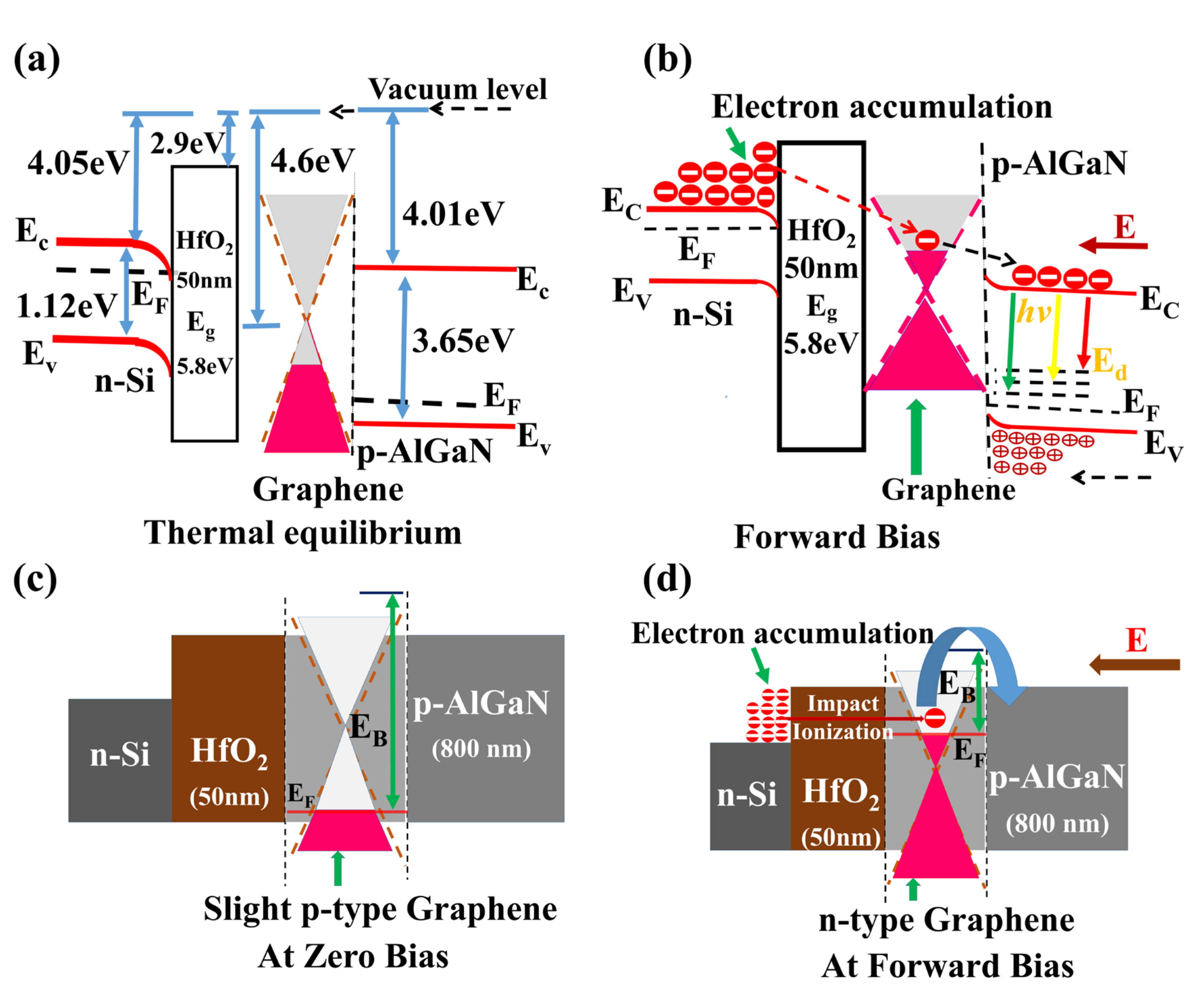
3. Results and Discussion
4. Conclusions
Supplementary Materials
Author Contributions
Funding
Conflicts of Interest
References
- Nakamura, S.; Harada, Y.; Senoh, M. Novel metalorganic chemical vapor deposition system for GaN growth. Appl. Phys. Lett. 1991, 58, 2021–2023. [Google Scholar] [CrossRef]
- Nakamura, S.; Iwasa, N.; Senoh, M.; Mukai, T. Hole Compensation Mechanism of P-Type GaN Films. Jpn. J. Appl. Phys. 1992, 31, 1258–1266. [Google Scholar] [CrossRef]
- Akasaki, I.; Amano, H. Crystal growth and conductivity control of group III nitride semiconductors and their application to short wavelength light emitters. Jpn. J. Appl. Phys. 1997, 36, 5393–5408. [Google Scholar] [CrossRef]
- Nakamura, S.; Mukai, T.; Senoh, M.; Iwasa, N. Thermal Annealing Effects on P-Type Mg-Doped GaN Films. Jpn. J. Appl. Phys. 1992, 31, L139–L142. [Google Scholar] [CrossRef]
- Ball, P. Let there be light. Nature 2001, 409, 974–976. [Google Scholar] [CrossRef] [PubMed]
- Leong, D.; Harry, M.; Reeson, K.J.; Homewood, K.P. A silicon/iron disilicide light-emitting diode operating at a wavelength of 1.5 mm. Nature 1997, 387, 686–688. [Google Scholar] [CrossRef]
- Ng, W.L.; Lourenç, M.A.; Gwilliam, R.M.; Ledain, S.; Shao, G.; Homewood, K.P. An efficient room-temperature silicon-based light-emitting diode. Nature 2001, 410, 192–194. [Google Scholar] [CrossRef]
- Hirschman, K.D.; Tybekov, L.; Duttagupta, S.P.; Fauchet, P.M. Silicon-based visible light-emitting devices integrated into microelectronic circuits. Nature 1996, 384, 338–341. [Google Scholar] [CrossRef]
- Castagna, M.E.; Coffa, S.; Monaco, M.; Muscara, A.; Caristia, L.; Lorenti, S.; Messina, A. High efficiency light emitting devices in silicon. Mater. Sci. Eng. B 2003, 105, 83–90. [Google Scholar] [CrossRef]
- Michael, K.; Jens, R. III-Nitride Ultraviolet Emitters, 1st ed.; Springer: Cham, Switzerland, 2016. [Google Scholar]
- Philip, M.R.; Choudhary, D.D.; Djavid, M.; Le, K.Q.; Piao, J.; Nguye, H.P.T. High efficiency green/yellow and red InGaN/AlGaN nanowire light-emitting diodes grown by molecular beam epitaxy. J. Sci. Adv. Mater. Devices 2017, 2, 150–155. [Google Scholar] [CrossRef]
- Feng, S.; Dong, B.; Lu, Y.; Yin, L.; Wei, B.; Wang, J.; Lin, S. Graphene/p-AlGaN/p-GaN electron tunnelling light emitting diodes with high external quantum efficiency. Nano Energy 2019, 60, 836–840. [Google Scholar] [CrossRef]
- Novoselov, K.S.; Jiang, D.; Schedin, F.; Booth, T.J.; Khotkevich, V.V.; Morozov, S.V.; Geim, A.K. Two-dimensional atomic crystals. Proc. Natl. Acad. Sci. USA 2005, 102, 10451–10453. [Google Scholar] [CrossRef] [PubMed]
- Novoselov, K.S.; Geim, A.K.; Morozov, S.V.; Jiang, D.; Zhang, Y.; Dubonos, S.V.; Grigorieva, I.V.; Firsov, A.A. Electric Field Effect in Atomically Thin Carbon Films. Science 2004, 306, 666–669. [Google Scholar] [CrossRef] [PubMed]
- Geim, A.K.; Grigorieva, I.V. Van der Waals heterostructures. Nature 2013, 499, 419–425. [Google Scholar] [CrossRef]
- Wang, L.; Liu, W.; Zhang, Y.; Zhang, Z.–H.; Tan, S.T.; Wang, G.; Sun, X.; Zhu, H.; Demir, H.V. Graphene-Based Transparent Conductive Electrodes for GaN-Based Light Emitting Diodes: Challenges and Countermeasures. Nano Energy 2015, 12, 419–436. [Google Scholar] [CrossRef]
- Khrapach, I.; Withers, F.; Bointon, H.T.; Polyushkin, D.K.; Barnes, W.L.; Russo, S.; Craciun, M.F. Novel Highly Conductive and Transparent Graphene-Based Conductors. Adv. Mater. 2012, 24, 2844–2849. [Google Scholar] [CrossRef]
- Hoiaas, I.M.; Mulyo, A.L.; Vullum, P.E.; Kim, D.–C.; Ahtapodov, L.; Fimland, B.–O.; Kishino, K.; Weman, H. GaN/AlGaN Nanocolumn Ultraviolet Light-Emitting Diode Using Double-Layer Graphene as Substrate and Transparent Electrode. Nano Lett. 2019, 19, 1649–1658. [Google Scholar] [CrossRef]
- Cao, Y.; Fatemi, V.; Demir, A.; Fang, S.; Tomarken, S.L.; Luo, J.Y.; Javier, D.; Watanabe, K.; Taniguchi, T.; Kaxiras, E.; et al. Correlated insulator behaviour at half-filling in magic-angle graphene superlattices. Nature 2018, 556, 26154. [Google Scholar] [CrossRef]
- Winzer, T.; Malić, E. Impact of Auger processes on carrier dynamics in graphene. Phys. Rev. B 2012, 85, 241404. [Google Scholar] [CrossRef]
- Gabor, N.M. Impact Excitation and Electron-Hole Multiplication in Graphene and Carbon Nanotubes. Acc. Chem. Res. 2013, 46, 1348–1357. [Google Scholar] [CrossRef]
- Park, H.; Fang, A.W.; Kodama, S.; Bowers, J.E. Hybrid silicon evanescent laser fabricated with a silicon waveguide and III-V offset quantum wells. Opt. Express. 2005, 13, 9460. [Google Scholar] [CrossRef] [PubMed]
- Philip, M.R.; Choudhary, D.D.; Djavid, M.; Bhuyian, M.N.; Piao, J.; Pham, T.T.; Misra, D.; Nguyen, H.P.T. Controlling color emission of InGaN/AlGaN nanowire light-emitting diodes grown by molecular beam epitaxy. J. Vac. Sci. Technol. B 2017, 35, 02B108-1–02B108-5. [Google Scholar] [CrossRef]
- Motohisa, J.; Kameda, H.; Sasaki, M.; Tomioka, K. Characterization of nanowire light-emitting diodes grown by selective-area metal-organic vapor-phase epitaxy. Nanotechnology 2019, 30, 134002. [Google Scholar] [CrossRef] [PubMed]
- Liu, Y.; Huang, Y.; Duan, X. Van der Waals integration before and beyond two-dimensional materials. Nature 2019, 567, 323–333. [Google Scholar] [CrossRef]
- Liu, Y.; Wang, P.; Wang, Y.; Lin, Z.; Liu, H.; Huang, J.; Huang, Y.; Duan, X. Van der Waals Integrated Devices Based on Nanomembranes of 3D Materials. Nano Lett. 2020, 20, 1410–1416. [Google Scholar] [CrossRef]
- McNeill, D.W.; Bhattacharya, S.; Wadsworth, H.; Ruddell, F.H.; Mitchell, S.J.N.; Armstrong, B.M.; Gamble, H.S. Atomic layer deposition of hafnium oxide dielectrics on silicon and germanium substrates. J. Mater. Sci. Mater. Electron. 2008, 19, 119–123. [Google Scholar] [CrossRef]
- Balkan, N.; Teke, A.; Gupta, R.; Straw, A.; Wolter, J.H.; Vleuten, W.v.d. Tunable wavelength hot electron light emitter. Appl. Phys. Lett. 1995, 67, 935–937. [Google Scholar] [CrossRef]
- Lee, H.; Paeng, K.; Kim, I.S. A review of doping modulation in graphene. Synth. Met. 2018, 244, 36–47. [Google Scholar] [CrossRef]
- Kwon, K.C.; Kim, S.Y. Extended thermal stability in metal-chloride doped graphene using graphene overlayers. Chem. Eng. Sci. 2014, 244, 355–363. [Google Scholar] [CrossRef]
- Dub, M.; Sai, P.; Przewłoka, A.; Krajewska, A.; Sakowicz, M.; Prystawko, P.; Kacperski, J.; Pasternak, I.; But, D.; Knap, W.; et al. Graphene as a Schottky Barrier Contact to AlGaN/GaN Heterostructures. Materials 2020, 13, 4140. [Google Scholar] [CrossRef]
- Park, P.S.; Reddy, K.M.; Nath, D.N.; Padture, N.P.; Rajan, S. Electrical Properties of Graphene/AlGaN/GaN Heterostructures. Mater. Sci. Forum. 2015, 821, 986–989. [Google Scholar]
- Pandit, B.; Seo, T.H.; Ryu, B.D.; Cho, J. Current transport mechanism in graphene/AlGaN/GaN heterostructures with various Al mole fractions. AIP Adv. 2016, 6, 065007. [Google Scholar] [CrossRef]
- Liao, L.; Bai, J.; Cheng, R.; Lin, Y.–C.; Jiang, S.; Qu, Y.; Huang, Y.; Duan, X. Sub-100 nm Channel Length Graphene Transistors. Nano Lett. 2010, 10, 3952–3956. [Google Scholar] [CrossRef] [PubMed]
- Dervos, C.; Bourkas, P.D.; Kagarakis, C.A. Charge transport trough a ‘‘metal-thick insulator metal’’ structure during impulse voltage excitation. J. Electrostat. 1991, 26, 121–132. [Google Scholar] [CrossRef]
- Kanitz, S. Charge transport in thick SiO2-based dielectric layers. Solid State Electron. 1997, 41, 1895–1902. [Google Scholar] [CrossRef]
- Nakamura, K.; Takahashi, T. An Observation of Breakdown Characteristics on Thick Silicon Oxide. In Proceedings of the 1995 ISPSD, Yokohama, Japan, 23–25 May 1995; ISBN 0-7803-2618-0. [Google Scholar]
- Hwang, W.; Kim, Y.K.; Rudd, M.E. New model for electron-impact ionization cross sections of molecules. J. Chem. Phys. 1996, 104, 2956–2966. [Google Scholar] [CrossRef]
- Jobst, J.; Waldmann, D.; Gornyi, I.V.; Mirlin, A.D.; Weber, H.B. Electron-Electron Interaction in the Magnetoresistance of Graphene. PRL 2012, 108, 106601. [Google Scholar] [CrossRef]
- Bolotin, K.I.; Ghahari, F.; Shulman, M.D.; Stormer, H.L.; Kim, P. Observation of the fractional quantum Hall effect in graphene. Nature 2009, 462, 196–199. [Google Scholar] [CrossRef]
- Du, X.; Skachko, I.; Duerr, F.; Luican, A.; Andrei, E.Y. Fractional quantum Hall effect and insulating phase of Dirac electrons in graphene. Nature 2009, 462, 192–195. [Google Scholar] [CrossRef]
- Morozov, S.V.; Novoselov, K.S.; Katsnelson, M.I.; Schedin, F.; Elias, D.C.; Jaszczak, J.A.; Geim, A.K. Giant Intrinsic Carrier Mobilities in Graphene and Its Bilayer. PRL 2008, 100, 016602. [Google Scholar] [CrossRef] [PubMed]
- Bolotin, K.I. Electronic transport in graphene: Towards high mobility. In Graphene: Properties, Preparation, Characterisation and Devices (Woodhead Publishing Series in Electronic and Optical Materials), 1st ed.; Viera, S., Kaiser, A.B., Eds.; Woodhead Publishing Limited: Cambridge, UK, 2014; pp. 199–227. ISBN 13-978-0857095084. [Google Scholar]
- Kim, Y.D.; Kim, H.; Cho, Y.; Ryoo, I.H.; Park, Y.D.; Kim, P.; Kim, Y.S.; Lee, S.; Li, Y.; Park, S.-N.; et al. Bright visible light emission from graphene. Nat. Nanotechnol 2015, 10, 676–681. [Google Scholar] [CrossRef] [PubMed]
- Gabor, N.M.; Song, J.C.W.; Ma, Q.; Nair, N.L.; Taychatanapat, T.; Watanabe, K.; Taniguchi, T.; Levitov, L.S.; Herrero, P.J. Hot Carrier–Assisted Intrinsic Photoresponse in Graphene. Science 2011, 334, 648–652. [Google Scholar] [CrossRef] [PubMed]
- Yu, Y.–J.; Zhao, Y.; Ryu, S.; Brus, L.E.; Kim, K.S.; Kim, P. Tuning the Graphene Work Function by Electric Field Effect. Nano Lett. 2009, 9, 3430–3434. [Google Scholar] [CrossRef]
- Chang, C.–W.; Tan, W.–C.; Lu, M.–L.; Pan, T.–C.; Yang, Y.–J.; Chen, Y.–F. Graphene/SiO2/p-GaN Diodes: An Advanced Economical Alternative for Electrically Tunable Light Emitters. Adv. Funct. Mater. 2013, 23, 4043–4048. [Google Scholar] [CrossRef]
- Yang, H.; Heo, J.; Park, S.; Song, H.J.; Seo, D.H.; Byun, K.–E.; Kim, P.; Yoo, I.K.; Chung, H.–J.; Kim, K. Graphene Barristor, a Triode Device with a Gate-Controlled Schottky Barrier. Science 2012, 336, 1140. [Google Scholar] [CrossRef]
- Sun, Y.; Sun, M.; Xie, D. Graphene Electronic Devices. Graphene: Fabrication, Characterizations, Properties and Applications, 1st ed.; Hongwei, Z., Zhiping, X., Dan, X., Ying, F., Eds.; Academic Press: Waltham, MA, USA, 2018; pp. 103–155. [Google Scholar]


Publisher’s Note: MDPI stays neutral with regard to jurisdictional claims in published maps and institutional affiliations. |
© 2020 by the authors. Licensee MDPI, Basel, Switzerland. This article is an open access article distributed under the terms and conditions of the Creative Commons Attribution (CC BY) license (http://creativecommons.org/licenses/by/4.0/).
Share and Cite
Manjunath, N.K.; Liu, C.; Lu, Y.; Yu, X.; Lin, S. Van der Waals Integrated Silicon/Graphene/AlGaN Based Vertical Heterostructured Hot Electron Light Emitting Diodes. Nanomaterials 2020, 10, 2568. https://doi.org/10.3390/nano10122568
Manjunath NK, Liu C, Lu Y, Yu X, Lin S. Van der Waals Integrated Silicon/Graphene/AlGaN Based Vertical Heterostructured Hot Electron Light Emitting Diodes. Nanomaterials. 2020; 10(12):2568. https://doi.org/10.3390/nano10122568
Chicago/Turabian StyleManjunath, Nallappagari Krishnamurthy, Chang Liu, Yanghua Lu, Xutao Yu, and Shisheng Lin. 2020. "Van der Waals Integrated Silicon/Graphene/AlGaN Based Vertical Heterostructured Hot Electron Light Emitting Diodes" Nanomaterials 10, no. 12: 2568. https://doi.org/10.3390/nano10122568
APA StyleManjunath, N. K., Liu, C., Lu, Y., Yu, X., & Lin, S. (2020). Van der Waals Integrated Silicon/Graphene/AlGaN Based Vertical Heterostructured Hot Electron Light Emitting Diodes. Nanomaterials, 10(12), 2568. https://doi.org/10.3390/nano10122568