Laser Printing of Plasmonic Nanosponges

 ,
,  , and
, and 
Abstract
1. Introduction
2. Materials and Methods
2.1. Deposition of Au Films Assisted with Various Discharge Gases
2.2. Characterization of Au Films
2.3. Fabrication of Porous Nanostructures and Nanosponges
2.4. Characterization of Laser-Printed Nanostructures
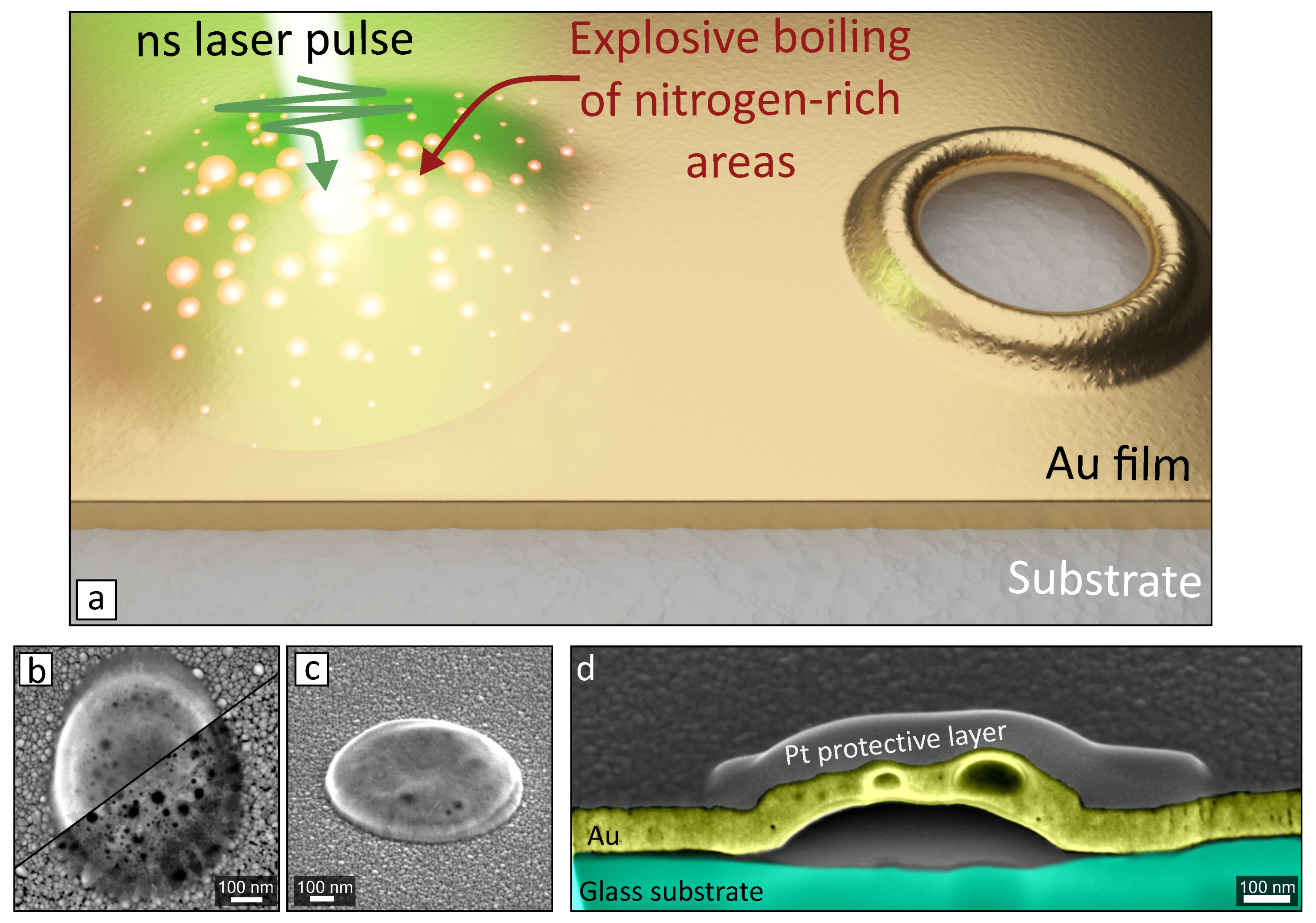
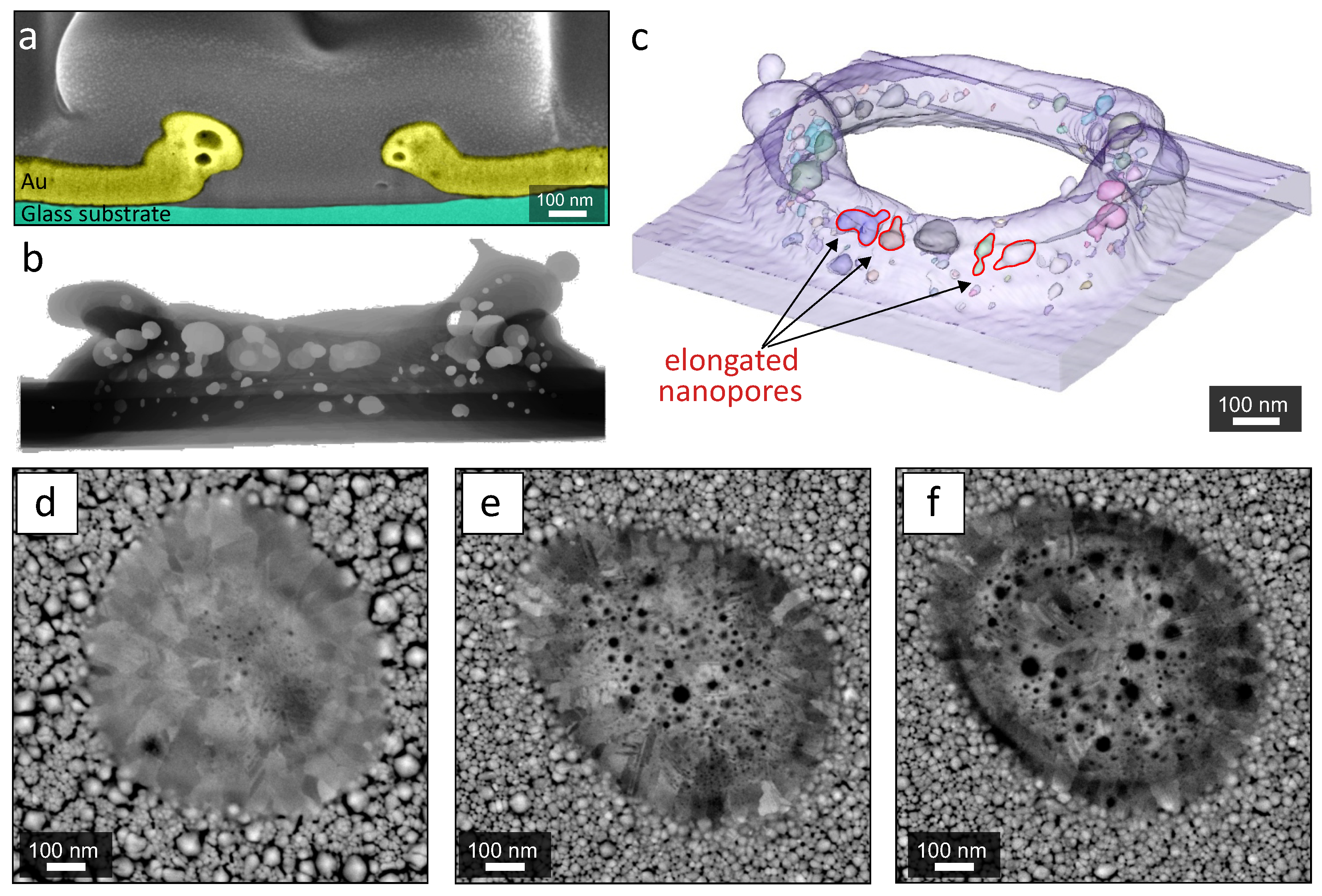
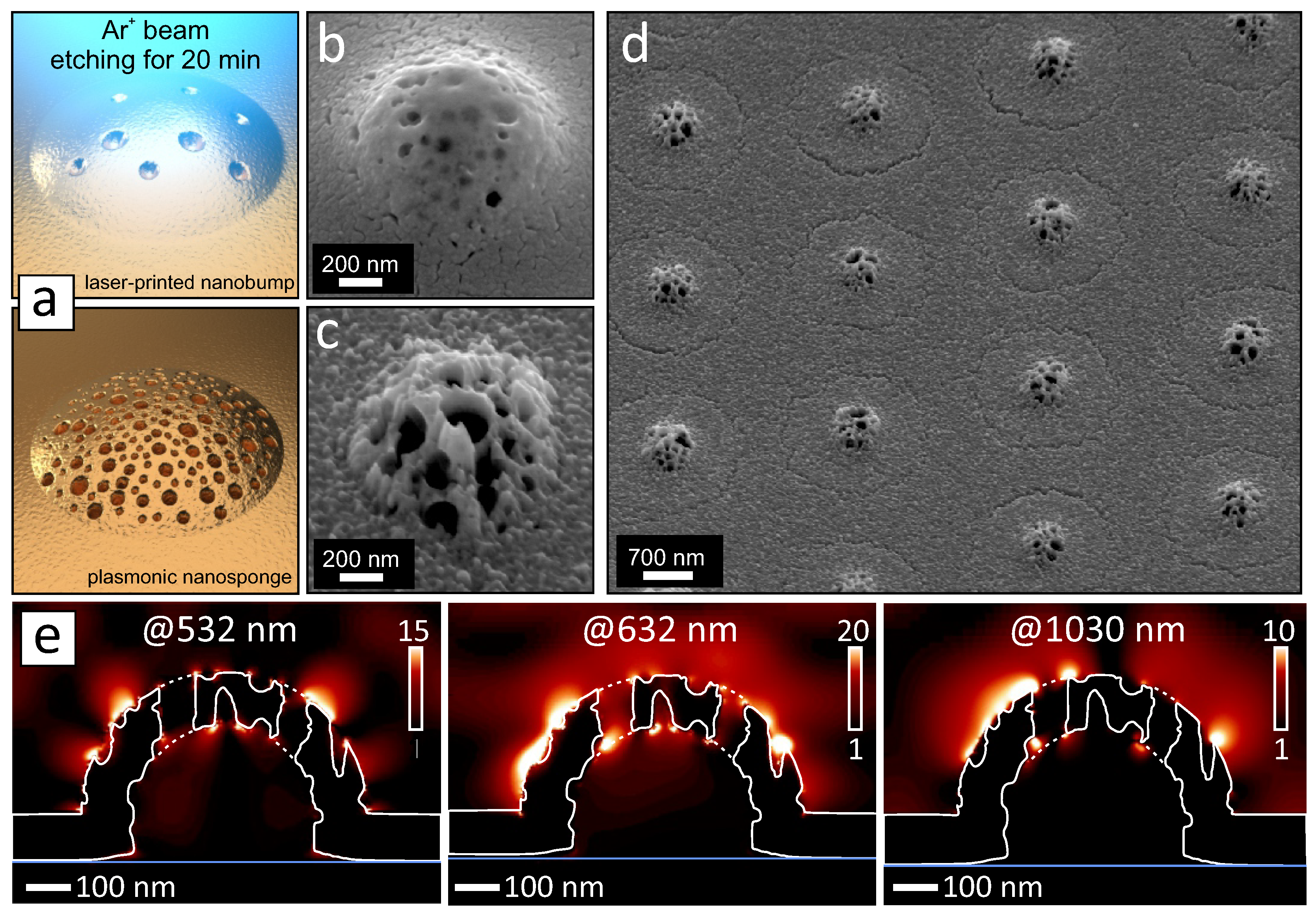
3. Results and Discussion
4. Conclusions and Outlook
Author Contributions
Funding
Conflicts of Interest
References
- Ryu, Y.; Kang, G.; Lee, C.W.; Kim, K. Porous metallic nanocone arrays for high-density SERS hot spots via solvent-assisted nanoimprint lithography of block copolymer. RSC Adv. 2015, 5, 76085–76091. [Google Scholar] [CrossRef]
- Liu, G.; Li, K.; Zhang, Y.; Du, J.; Ghafoor, S.; Lu, Y. A facile periodic porous Au nanoparticle array with high-density and built-in hotspots for SERS analysis. Appl. Surf. Sci. 2020, 5, 146807. [Google Scholar] [CrossRef]
- Zhang, T.; Bai, Y.; Sun, Y.; Hang, L.; Li, X.; Liu, D.; Lyu, X.; Li, C.; Cai, W.; Li, Y. Laser-irradiation induced synthesis of spongy AuAgPt alloy nanospheres with high-index facets, rich grain boundaries and subtle lattice distortion for enhanced electrocatalytic activity. J. Mat. Chem. A 2018, 6, 13735–13742. [Google Scholar] [CrossRef]
- Eid, K.; Wang, H.; Malgras, V.; Alothman, Z.; Yamauchi, Y.; Wang, L. Trimetallic PtPdRu Dendritic Nanocages with Three-Dimensional Electrocatalytic Surfaces. J. Phys. Chem. C 2015, 119, 19947–19953. [Google Scholar] [CrossRef]
- Santos, G.; Ferrara, F.; Zhao, F.; Rodrigues, D.; Shih, W. Photothermal inactivation of heat-resistant bacteria on nanoporous gold disk arrays. Opt. Mater. Express 2016, 6, 1217–1229. [Google Scholar] [CrossRef]
- Vidal, C.; Sivun, D.; Ziegler, J.; Wang, D.; Schaaf, P.; Hrelescu, C.; Klar, T.A. Plasmonic Horizon in Gold Nanosponges. Nano Lett. 2018, 18, 1269–1273. [Google Scholar] [CrossRef]
- Vidal, C.; Wang, D.; Schaaf, P.; Hrelescu, C.; Klar, T.A. Optical Plasmons of Individual Gold Nanosponges. ACS Photonics 2015, 2, 1436–1442. [Google Scholar] [CrossRef]
- Hergert, G.; Vogelsang, J.; Schwarz, F.; Wang, D.; Kollmann, H.; Groß, P.; Lienau, C.; Runge, E.; Schaaf, P. Long-lived electron emission reveals localized plasmon modes in disordered nanosponge antennas. Light Sci. Appl. 2017, 6, e17075. [Google Scholar] [CrossRef]
- Zhang, X.; Zheng, Y.; Liu, X.; Lu, W.; Dai, J.; Lei, D.; MacFarlane, D. Hierarchical Porous Plasmonic Metamaterials for Reproducible Ultrasensitive Surface—Enhanced Raman Spectroscopy. Adv. Mater. 2015, 6, 1090–1096. [Google Scholar] [CrossRef]
- Zhong, J.; Chimeh, A.; Korte, A.; Schwarz, F.; Yi, J.; Wang, D.; Zhan, J.; Schaaf, P.; Runge, E.; Lienau, C. Strong Spatial and Spectral Localization of Surface Plasmons in Individual Randomly Disordered Gold Nanosponges. Nano Lett. 2018, 18, 4957–4964. [Google Scholar] [CrossRef]
- Genç, A.; Patarroyo, J.; Sancho-Parramon, J.; Arenal, R.; Duchamp, M.; Gonzalez, E.; Henrard, L.; Bastùs, N.; Dunin-Borkowski, R.; Puntes, V.; et al. Tuning the Plasmonic Response up: Hollow Cuboid Metal Nanostructures. ACS Photonics 2016, 3, 770–779. [Google Scholar] [CrossRef]
- Garcia-Leis, A.; Torreggiani, A.; Garcia-Ramos, J.; Sanchez-Cortes, S. Hollow Au/Ag nanostars displaying broad plasmonic resonance and high surface-enhanced Raman sensitivity. Nanoscale 2015, 7, 13629–13637. [Google Scholar] [CrossRef]
- Schubert, I.; Huck, C.; Kröber, F.P.; Neubrech, F.; Pucci, A.; Toimil-Molares, M.; Trautmann, C.; Vogt, J. Porous Gold Nanowires: Plasmonic Response and Surface—Enhanced Infrared Absorption. Adv. Opt. Mater. 2016, 4, 1838–1845. [Google Scholar] [CrossRef]
- Garoli, D.; Calandrini, E.; Bozzola, A.; Ortolani, M.; Cattarin, S.; Barison, S.; Tomaa, A.; Angelis, F.D. Boosting infrared energy transfer in 3D nanoporous gold antennas. Nanoscale 2017, 9, 915–922. [Google Scholar] [CrossRef]
- Syubaev, S.; Nepomnyashchiy, A.; Mitsai, E.; Pustovalov, E.; Vitrik, O.; Kudryashov, S.; Kuchmizhak, A. Fabrication of porous microrings via laser printing and ion-beam post-etching. Appl. Phys. Lett. 2017, 111, 083102. [Google Scholar] [CrossRef]
- Li, K.; Liu, G.; Zhang, S.; Dai, Y.; Ghafoor, S.; Huang, W.; Zu, Z.; Lu, Y. A porous Au–Ag hybrid nanoparticle array with broadband absorption and high-density hotspots for stable SERS analysis. Nanoscale 2019, 11, 9587–9592. [Google Scholar] [CrossRef]
- Calandrini, E.; Giovannini, G.; Garoli, D. 3D nanoporous antennas as a platform for high sensitivity IR plasmonic sensing. Opt. Express 2019, 27, 25912–25919. [Google Scholar] [CrossRef]
- Ruffino, F.; Grimaldi, M.G. Nanoporous Gold-Based Sensing. Coatings 2020, 10, 899. [Google Scholar] [CrossRef]
- Rao, W.; Wang, D.; Kups, T.; Baradács, E.; Parditka, B.; Erdélyi, Z.; Schaaf, P. Nanoporous Gold Nanoparticles and Au/Al2O3 Hybrid Nanoparticles with Large Tunability of Plasmonic Properties. ACS Appl. Mater. Interfaces 2017, 9, 6273–6281. [Google Scholar] [CrossRef]
- Schwarz, F.; Runge, E. Towards Optimal Disorder in Gold Nanosponges for Long?Lived Localized Plasmonic Modes. Ann. Phys. 2017, 529, 1600234. [Google Scholar] [CrossRef]
- Liu, K.; Bai, Y.; Zhang, L.; Yang, Z.; Fan, Q.; Zheng, H.; Yin, Y.; Gao, C. Porous Au–Ag nanospheres with high-density and highly accessible hotspots for SERS analysis. Nano Lett. 2016, 16, 3675–3681. [Google Scholar] [CrossRef] [PubMed]
- Li, G.G.; Lin, Y.; Wang, H. Residual silver remarkably enhances electrocatalytic activity and durability of dealloyed gold nanosponge particles. Nano Lett. 2016, 16, 7248–7253. [Google Scholar] [CrossRef] [PubMed]
- Jiang, B.; Li, C.; Tang, J.; Takei, T.; Kim, J.H.; Ide, Y.; Henzie, J.; Tominaka, S.; Yamauchi, Y. Tunable-Sized Polymeric Micelles and Their Assembly for the Preparation of Large Mesoporous Platinum Nanoparticles. Angew. Chem. Int. Ed. 2016, 55, 10037–10041. [Google Scholar] [CrossRef]
- Jiang, B.; Li, C.; Imura, M.; Tang, J.; Yamauchi, Y. Multimetallic mesoporous spheres through surfactant?directed synthesis. Adv. Sci. 2015, 2, 1500112. [Google Scholar] [CrossRef]
- Jiang, B.; Li, C.; Dag, Ö.; Abe, H.; Takei, T.; Imai, T.; Hossain, M.S.A.; Islam, M.T.; Wood, K.; Henzie, J.; et al. Mesoporous metallic rhodium nanoparticles. Nat. Commun. 2017, 8, 1–8. [Google Scholar] [CrossRef]
- Wang, H.; Jeong, H.Y.; Imura, M.; Wang, L.; Radhakrishnan, L.; Fujita, N.; Castle, T.; Terasaki, O.; Yamauchi, Y. Shape-and size-controlled synthesis in hard templates: sophisticated chemical reduction for mesoporous monocrystalline platinum nanoparticles. J. Am. Chem. Soc. 2011, 133, 14526–14529. [Google Scholar] [CrossRef]
- Kani, K.; Malgras, V.; Jiang, B.; Hossain, M.S.A.; Alshehri, S.M.; Ahamad, T.; Salunkhe, R.R.; Huang, Z.; Yamauchi, Y. Periodically Arranged Arrays of Dendritic Pt Nanospheres Using Cage?Type Mesoporous Silica as a Hard Template. Chem. Asian J. 2018, 13, 106–110. [Google Scholar] [CrossRef]
- Zhang, Q.; Large, N.; Nordlander, P.; Wang, H. Porous Au Nanoparticles with Tunable Plasmon Resonances and Intense Field Enhancements for Single-Particle SERS. J. Phys. Chem. Lett. 2014, 5, 370–374. [Google Scholar] [CrossRef]
- Arnob, M.M.P.; Zhao, F.; Li, J.; Shih, W.C. EBL-based fabrication and different modeling approaches for nanoporous gold nanodisks. ACS Photonics 2017, 4, 1870–1878. [Google Scholar] [CrossRef]
- Kuchmizhak, A.; Gurbatov, S.; Vitrik, O.; Kulchin, Y.; Milichko, V.; Makarov, S.; Kudryashov, S. Ion-beam assisted laser fabrication of sensing plasmonic nanostructures. Sci. Rep. 2016, 6, 19410. [Google Scholar] [CrossRef]
- Babar, S.; Weaver, J. Optical constants of Cu, Ag, and Au revisited. Appl. Opt. 2015, 54, 477–481. [Google Scholar] [CrossRef]
- Meshcheryakov, Y.P.; Bulgakova, N.M. Thermoelastic modeling of microbump and nanojet formation on nanosize gold films under femtosecond laser irradiation. Appl. Phys. A 2006, 82, 363. [Google Scholar] [CrossRef]
- Wang, X.W.; Kuchmizhak, A.A.; Li, X.; Juodkazis, S.; Vitrik, O.B.; Kulchin, Y.N.; Zhakhovsky, V.V.; Danilov, P.A.; Ionin, A.A.; Kudryashov, S.I.; et al. Laser-induced translative hydrodynamic mass snapshots: noninvasive characterization and predictive modeling via mapping at nanoscale. Phys. Rev. Appl. 2017, 8, 044016. [Google Scholar] [CrossRef]
- Liu, J.M. Simple technique for measurements of pulsed Gaussian-beam spot sizes. Opt. Lett. 1982, 7, 196–198. [Google Scholar] [CrossRef] [PubMed]
- Garcia-Lechuga, M.; Gebrayel El Reaidy, G.; Ning, H.; Delaporte, P.; Grojo, D. Assessing the limits of determinism and precision in ultrafast laser ablation. Appl. Phys. Lett. 2020, 117, 171604. [Google Scholar] [CrossRef]
- Fang, Z.; Zhen, Y.R.; Neumann, O.; Polman, A.; García de Abajo, F.J.; Nordlander, P.; Halas, N.J. Evolution of Light-Induced Vapor Generation at a Liquid-Immersed Metallic Nanoparticle. Nano Lett. 2013, 13, 1736–1742. [Google Scholar] [CrossRef] [PubMed]
- Wang, Y.; Zaytsev, M.E.; The, H.L.; Eijkel, J.C.T.; Zandvliet, H.J.W.; Zhang, X.; Lohse, D. Vapor and Gas-Bubble Growth Dynamics around Laser-Irradiated, Water-Immersed Plasmonic Nanoparticles. ACS Nano 2017, 11, 2045–2051. [Google Scholar] [CrossRef] [PubMed]
- Iida, T.; Guthrie, R.I.L. The Physical Properties of Liquid Metals; Oxford University Press: New York, NY, USA, 1993. [Google Scholar]
- Kneier, F.; Geldhauser, T.; Scheer, E.; Leiderer, P.; Boneberg, J. Nanosecond laser pulse induced vertical movement of thin gold films on silicon determined by a modified Michelson interferometer. Appl. Phys. A 2013, 110, 321–327. [Google Scholar] [CrossRef]
- Kulchin, Y.N.; Vitrik, O.B.; Kuchmizhak, A.A.; Nepomnyashchii, A.V.; Savchuk, A.G.; Ionin, A.A.; Kudryashov, S.I.; Makarov, S.V. Through nanohole formation in thin metallic film by single nanosecond laser pulses using optical dielectric apertureless probe. Opt. Lett. 2013, 38, 1452–1454. [Google Scholar] [CrossRef]
- Šiller, L.; Hunt, M.R.C.; Brown, J.W.; Coquel, J.M.; Rudolf, P. Nitrogen ion irradiation of Au (110): formation of gold nitride. Surf. Sci. 2002, 513, 78–82. [Google Scholar] [CrossRef]
- Caricato, A.P.; Fernandez, M.; Leggieri, G.; Luches, A.; Martino, M.; Romano, F.; Tunno, T.; Valerini, D.; Verdyan, A.; Soifer, Y.M.; et al. Reactive pulsed laser deposition of gold nitride thin films. Appl. Surf. Sci. 2007, 253, 8037–8040. [Google Scholar] [CrossRef]
- Devia, A.; Castillo, H.A.; Benavides, V.J.; Arango, Y.C.; Quintero, J.H. Growth and characterization of AuN films through the pulsed arc technique. Mater. Charact. 2008, 59, 105–107. [Google Scholar] [CrossRef]
- Šiller, L.; Peltekis, N.; Krishnamurthy, S.; Chao, Y.; Bull, S.J.; Hunt, M.R.C. Gold film with gold nitride—A conductor but harder than gold. Appl. Phys. Lett. 2005, 86, 221912. [Google Scholar] [CrossRef]
- Krishnamurthy, S.; Montalti, M.; Wardle, M.G.; Shaw, M.J.; Briddon, P.R.; Svensson, K.; Hunt, M.R.C.; Šiller, L. Nitrogen ion irradiation of Au (110): Photoemission spectroscopy and possible crystal structures of gold nitride. Phys. Rev. B 2004, 70, 045414. [Google Scholar] [CrossRef]
- Pavliuk, G.; Pavlov, D.; Mitsai, E.; Vitrik, O.; Mironenko, A.; Zakharenko, A.; Kulinich, S.A.; Juodkazis, S.; Bratskaya, S.; Zhizhchenko, A.; et al. Ultrasensitive SERS-Based Plasmonic Sensor with Analyte Enrichment System Produced by Direct Laser Writing. Nanomaterials 2020, 10, 49. [Google Scholar] [CrossRef]
- Naghilou, A.; He, M.; Schubert, J.S.; Zhigilei, L.V.; Kautek, W. Femtosecond laser generation of microbumps and nanojets on single and bilayer Cu/Ag thin films. Phys. Chem. Chem. Phys. 2019, 21, 11846–11860. [Google Scholar] [CrossRef]
- Zhang, Y.; Grady, N.K.; Ayala-Orozco, C.; Halas, N.J. Three-dimensional nanostructures as highly efficient generators of second harmonic light. Nano Lett. 2011, 11, 5519–5523. [Google Scholar] [CrossRef]
- Butet, J.; Brevet, P.F.; Martin, O.J.F. Optical second harmonic generation in plasmonic nanostructures: From fundamental principles to advanced applications. ACS Nano 2015, 9, 10545–10562. [Google Scholar] [CrossRef]
- Makarov, S.V.; Zalogina, A.S.; Tajik, M.; Zuev, D.A.; Rybin, M.V.; Kuchmizhak, A.A.; Juodkazis, S.; Kivshar, Y. Light-Induced Tuning and Reconfiguration of Nanophotonic Structures. Laser Photonics Rev. 2017, 11, 1700108. [Google Scholar] [CrossRef]
- Cherepakhin, A.B.; Pavlov, D.V.; Shishkin, I.I.; Voroshilov, P.M.; Juodkazis, S.; Makarov, S.V.; Kuchmizhak, A.A. Laser-printed hollow nanostructures for nonlinear plasmonics. Appl. Phys. Lett. 2020, 117, 041108. [Google Scholar] [CrossRef]
- Baffou, G.; Cichos, F.; Quidant, R. Applications and challenges of thermoplasmonics. Nat. Mater. 2020, 19, 946–958. [Google Scholar] [CrossRef]
- Yi, J.M.; Wang, D.; Schwarz, F.; Zhong, J.; Chimeh, A.; Korte, A.; Zhan, J.; Schaaf, P.; Runge, E.; Lienau, C. Doubly Resonant Plasmonic Hot Spot—Exciton Coupling Enhances Second Harmonic Generation from Au/ZnO Hybrid Porous Nanosponges. ACS Photonics 2019, 6, 2779–2787. [Google Scholar] [CrossRef]
- Larin, A.O.; Nominé, A.; Ageev, E.I.; Ghanbaja, J.; Kolotova, L.N.; Starikov, S.V.; Bruyère, S.; Belmonte, T.; Makarov, S.V.; Zuev, D.A. Plasmonic nanosponges filled with silicon for enhanced white light emission. Nanoscale 2020, 12, 1013–1021. [Google Scholar] [CrossRef]
- Zhong, J.H.; Vogelsang, J.; Yi, J.M.; Wang, D.; Wittenbecher, L.; Mikaelsson, S.; Korte, A.; Chimeh, A.; Arnold, C.L.; Schaaf, P.; et al. Nonlinear plasmon-exciton coupling enhances sum-frequency generation from a hybrid metal/semiconductor nanostructure. Nat. Commun. 2020, 11, 1–10. [Google Scholar] [CrossRef]
- Hashimoto, Y.; Seniutinas, G.; Balčytis, A.; Juodkazis, S.; Nishijima, Y. Au-Ag-Cu nano-alloys: Tailoring of permittivity. Sci. Rep. 2016, 6, 25010. [Google Scholar] [CrossRef]
- Takenaka, M.; Hashimoto, Y.; Iwasa, T.; Taketsugu, T.; Seniutinas, G.; Balčytis, A.; Juodkazis, S.; Nishijima, Y. First Principles Calculations Toward Understanding SERS of 2, 2’-Bipyridyl Adsorbed on Au, Ag, and Au–Ag Nanoalloy. J. Comput. Chem. 2019, 40, 925–932. [Google Scholar] [CrossRef]
- George, E.P.; Raabe, D.; Ritchie, R.O. High-entropy alloys. Nat. Rev. Mater. 2019, 4, 515–534. [Google Scholar] [CrossRef]


Publisher’s Note: MDPI stays neutral with regard to jurisdictional claims in published maps and institutional affiliations. |
© 2020 by the authors. Licensee MDPI, Basel, Switzerland. This article is an open access article distributed under the terms and conditions of the Creative Commons Attribution (CC BY) license (http://creativecommons.org/licenses/by/4.0/).
Share and Cite
Syubaev, S.; Gurbatov, S.; Modin, E.; Linklater, D.P.; Juodkazis, S.; Gurevich, E.L.; Kuchmizhak, A. Laser Printing of Plasmonic Nanosponges. Nanomaterials 2020, 10, 2427. https://doi.org/10.3390/nano10122427
Syubaev S, Gurbatov S, Modin E, Linklater DP, Juodkazis S, Gurevich EL, Kuchmizhak A. Laser Printing of Plasmonic Nanosponges. Nanomaterials. 2020; 10(12):2427. https://doi.org/10.3390/nano10122427
Chicago/Turabian StyleSyubaev, Sergey, Stanislav Gurbatov, Evgeny Modin, Denver P. Linklater, Saulius Juodkazis, Evgeny L. Gurevich, and Aleksandr Kuchmizhak. 2020. "Laser Printing of Plasmonic Nanosponges" Nanomaterials 10, no. 12: 2427. https://doi.org/10.3390/nano10122427
APA StyleSyubaev, S., Gurbatov, S., Modin, E., Linklater, D. P., Juodkazis, S., Gurevich, E. L., & Kuchmizhak, A. (2020). Laser Printing of Plasmonic Nanosponges. Nanomaterials, 10(12), 2427. https://doi.org/10.3390/nano10122427