Electrostatic Design of Polar Metal–Organic Framework Thin Films


Abstract

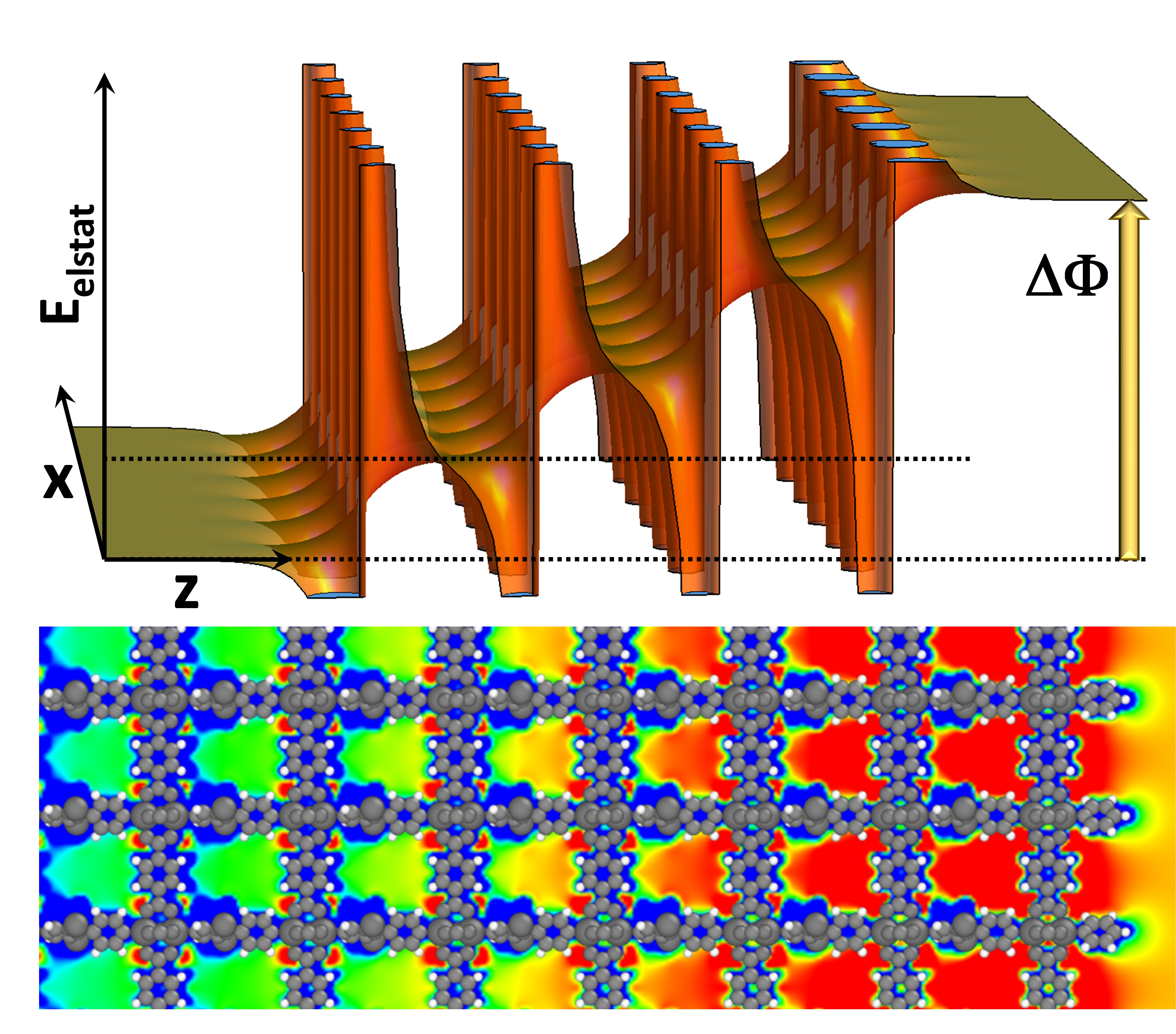
1. Introduction
2. Electronic Structure of a Polar MOF Thin Film
3. Materials and Methods
3.1. Computational Methodology
3.2. Suggesting a Strategy for Realizing a Polar MOF
4. Results and Discussion
4.1. Electronic Structure of the Polar MOF Thin Films
4.2. Aligning the Polar Linkers during MOF Growth—Bonding Asymmetry
5. Conclusions
Supplementary Materials
Author Contributions
Funding
Acknowledgments
Conflicts of Interest
References
- Furukawa, H.; Cordova, K.E.; O’Keeffe, M.; Yaghi, O.M. The chemistry and applications of metal-organic frameworks. Science 2013, 341, 1230444. [Google Scholar] [CrossRef] [PubMed]
- Moghadam, P.Z.; Li, A.; Liu, X.-W.; Bueno-Perez, R.; Wang, S.-D.; Wiggin, S.B.; Wood, P.A.; Fairen-Jimenez, D. Targeted classification of metal–organic frameworks in the Cambridge structural database (CSD). Chem. Sci. 2020, 11, 8373–8387. [Google Scholar] [CrossRef]
- Liu, J.; Chen, L.; Cui, H.; Zhang, J.; Zhang, L.; Su, C.Y. Applications of metal-organic frameworks in heterogeneous supramolecular catalysis. Chem. Soc. Rev. 2014, 43, 6011–6061. [Google Scholar] [CrossRef] [PubMed]
- Zhu, L.; Liu, X.Q.; Jiang, H.L.; Sun, L.B. Metal-Organic Frameworks for Heterogeneous Basic Catalysis. Chem. Rev. 2017, 117, 8129–8176. [Google Scholar] [CrossRef]
- Pascanu, V.; González Miera, G.; Inge, A.K.; Martín-Matute, B. Metal-Organic Frameworks as Catalysts for Organic Synthesis: A Critical Perspective. J. Am. Chem. Soc. 2019, 141, 7223–7234. [Google Scholar] [CrossRef]
- Eddaoudi, M.; Kim, J.; Rosi, N.; Vodak, D.; Wachter, J.; O’Keeffe, M.; Yaghi, O.M. Systematic design of pore size and functionality in isoreticular MOFs and their application in methane storage. Science 2002, 295, 469–472. [Google Scholar] [CrossRef]
- Rowsell, J.L.C.; Yaghi, O.M. Effects of functionalization, catenation, and variation of the metal oxide and organic linking units on the low-pressure hydrogen adsorption properties of metal-organic frameworks. J. Am. Chem. Soc. 2006, 128, 1304–1315. [Google Scholar] [CrossRef]
- Murray, L.J.; Dinc, M.; Long, J.R. Hydrogen storage in metal-organic frameworks. Chem. Soc. Rev. 2009, 38, 1294–1314. [Google Scholar] [CrossRef]
- Chen, B.; Liang, C.; Yang, J.; Contreras, D.S.; Clancy, Y.L.; Lobkovsky, E.B.; Yaghi, O.M.; Dai, S. A microporous metal-organic framework for gas-chromatographic separation of alkanes. Angew. Chem. Int. Ed. 2006, 45, 1390–1393. [Google Scholar] [CrossRef]
- Bloch, E.D.; Queen, W.L.; Krishna, R.; Zadrozny, J.M.; Brown, C.M.; Long, J.R. Hydrocarbon separations in a metal-organic framework with open iron(II) coordination sites. Science 2012, 335, 1606–1610. [Google Scholar] [CrossRef]
- Allendorf, M.D.; Bauer, C.A.; Bhakta, R.K.; Houk, R.J.T. Luminescent metal–organic frameworks. Chem. Soc. Rev. 2009, 38, 1330. [Google Scholar] [CrossRef] [PubMed]
- Stassen, I.; Burtch, N.; Talin, A.; Falcaro, P.; Allendorf, M.; Ameloot, R. An updated roadmap for the integration of metal–organic frameworks with electronic devices and chemical sensors. Chem. Soc. Rev. 2017, 46, 3185–3241. [Google Scholar] [CrossRef] [PubMed]
- Sun, L.; Campbell, M.G.; Dincă, M. Electrically Conductive Porous Metal–Organic Frameworks. Angew. Chem. Int. Ed. 2016, 55, 3566–3579. [Google Scholar] [CrossRef] [PubMed]
- Allendorf, M.D.; Foster, M.E.; Léonard, F.; Stavila, V.; Feng, P.L.; Doty, F.P.; Leong, K.; Ma, E.Y.; Johnston, S.R.; Talin, A.A. Guest-Induced Emergent Properties in Metal–Organic Frameworks. J. Phys. Chem. Lett. 2015, 6, 1182–1195. [Google Scholar] [CrossRef] [PubMed]
- Haldar, R.; Heinke, L.; Wöll, C. Advanced Photoresponsive Materials Using the Metal–Organic Framework Approach. Adv. Mater. 2020, 32, 1905227. [Google Scholar] [CrossRef] [PubMed]
- Kreno, L.E.; Leong, K.; Farha, O.K.; Allendorf, M.; Van Duyne, R.P.; Hupp, J.T. Metal-organic framework materials as chemical sensors. Chem. Rev. 2012, 112, 1105–1125. [Google Scholar] [CrossRef] [PubMed]
- Son, H.J.; Jin, S.; Patwardhan, S.; Wezenberg, S.J.; Jeong, N.C.; So, M.; Wilmer, C.E.; Sarjeant, A.A.; Schatz, G.C.; Snurr, R.Q.; et al. Light-harvesting and ultrafast energy migration in porphyrin-based metal-organic frameworks. J. Am. Chem. Soc. 2013, 135, 862–869. [Google Scholar] [CrossRef]
- Zhang, T.; Lin, W. Metal-organic frameworks for artificial photosynthesis and photocatalysis. Chem. Soc. Rev. 2014, 43, 5982–5993. [Google Scholar] [CrossRef]
- Oldenburg, M.; Turshatov, A.; Busko, D.; Wollgarten, S.; Adams, M.; Baroni, N.; Welle, A.; Redel, E.; Wöll, C.; Richards, B.S.; et al. Photon Upconversion at Crystalline Organic–Organic Heterojunctions. Adv. Mater. 2016, 28, 8477–8482. [Google Scholar] [CrossRef]
- Thomas, S.; Li, H.; Dasari, R.R.; Evans, A.M.; Castano, I.; Allen, T.G.; Reid, O.G.; Rumbles, G.; Dichtel, W.R.; Gianneschi, N.C.; et al. Design and synthesis of two-dimensional covalent organic frameworks with four-arm cores: Prediction of remarkable ambipolar charge-transport properties. Mater. Horiz. 2019, 6, 1868–1876. [Google Scholar] [CrossRef]
- Clough, A.J.; Orchanian, N.M.; Skelton, J.M.; Neer, A.J.; Howard, S.A.; Downes, C.A.; Piper, L.F.J.; Walsh, A.; Melot, B.C.; Marinescu, S.C. Room Temperature Metallic Conductivity in a Metal–Organic Framework Induced by Oxidation. J. Am. Chem. Soc. 2019, 141, 16323–16330. [Google Scholar] [CrossRef] [PubMed]
- Skorupskii, G.; Trump, B.A.; Kasel, T.W.; Brown, C.M.; Hendon, C.H.; Dincă, M. Efficient and tunable one-dimensional charge transport in layered lanthanide metal–organic frameworks. Nat. Chem. 2020, 12, 131–136. [Google Scholar] [CrossRef] [PubMed]
- Wang, M.; Ballabio, M.; Wang, M.; Lin, H.-H.; Biswal, B.P.; Han, X.; Paasch, S.; Brunner, E.; Liu, P.; Chen, M.; et al. Unveiling Electronic Properties in Metal–Phthalocyanine-Based Pyrazine-Linked Conjugated Two-Dimensional Covalent Organic Frameworks. J. Am. Chem. Soc. 2019, 141, 16810–16816. [Google Scholar] [CrossRef] [PubMed]
- Xie, L.S.; Skorupskii, G.; Dincă, M. Electrically Conductive Metal–Organic Frameworks. Chem. Rev. 2020, 120, 8536–8580. [Google Scholar] [CrossRef]
- Tamai, Y.; Ohkita, H.; Benten, H.; Ito, S. Exciton Diffusion in Conjugated Polymers: From Fundamental Understanding to Improvement in Photovoltaic Conversion Efficiency. J. Phys. Chem. Lett. 2015, 6, 3417–3428. [Google Scholar] [CrossRef]
- Menke, S.M.; Holmes, R.J. Exciton diffusion in organic photovoltaic cells. Energy Environ. Sci. 2014, 7, 499–512. [Google Scholar] [CrossRef]
- Zhang, Q.; Zhang, C.; Cao, L.; Wang, Z.; An, B.; Lin, Z.; Huang, R.; Zhang, Z.; Wang, C.; Lin, W. Förster Energy Transport in Metal-Organic Frameworks Is beyond Step-by-Step Hopping. J. Am. Chem. Soc. 2016, 138, 5308–5315. [Google Scholar] [CrossRef]
- Adams, M.; Kozlowska, M.; Baroni, N.; Oldenburg, M.; Ma, R.; Busko, D.; Turshatov, A.; Emandi, G.; Senge, M.O.; Haldar, R.; et al. Highly Efficient One-Dimensional Triplet Exciton Transport in a Palladium-Porphyrin-Based Surface-Anchored Metal-Organic Framework. ACS Appl. Mater. Interfaces 2019, 11, 15688–15697. [Google Scholar] [CrossRef]
- Kretz, B.; Egger, D.A.; Zojer, E. A Toolbox for Controlling the Energetics and Localization of Electronic States in Self-Assembled Organic Monolayers. Adv. Sci. 2015, 2, 1400016. [Google Scholar] [CrossRef]
- Obersteiner, V.; Jeindl, A.; Götz, J.; Perveaux, A.; Hofmann, O.T.; Zojer, E. Electrostatic Design of 3D Covalent Organic Networks. Adv. Mater. 2017, 29, 1700888. [Google Scholar] [CrossRef]
- Joshi, T.; Chen, C.; Li, H.; Diercks, C.S.; Wang, G.; Waller, P.J.; Li, H.; Bredas, J.-L.; Yaghi, O.M.; Crommie, M.F. Local Electronic Structure of Molecular Heterojunctions in a Single-Layer 2D Covalent Organic Framework. Adv. Mater. 2019, 31, 1805941. [Google Scholar] [CrossRef] [PubMed]
- Natan, A.; Kronik, L.; Haick, H.; Tung, R.T. Electrostatic Properties of Ideal and Non-ideal Polar Organic Monolayers: Implications for Electronic Devices. Adv. Mater. 2007, 19, 4103–4117. [Google Scholar] [CrossRef]
- Cahen, D.; Naaman, R.; Vager, Z. The Cooperative Molecular Field Effect. Adv. Funct. Mater. 2005, 15, 1571–1578. [Google Scholar] [CrossRef]
- Heimel, G.; Rissner, F.; Zojer, E. Modeling the Electronic Properties of π-Conjugated Self-Assembled Monolayers. Adv. Mater. 2010, 22, 2494–2513. [Google Scholar] [CrossRef] [PubMed]
- Monti, O.L.A. Understanding Interfacial Electronic Structure and Charge Transfer: An Electrostatic Perspective. J. Phys. Chem. Lett. 2012, 3, 2342–2351. [Google Scholar] [CrossRef] [PubMed]
- Zojer, E.; Taucher, T.C.; Hofmann, O.T. The Impact of Dipolar Layers on the Electronic Properties of Organic/Inorganic Hybrid Interfaces. Adv. Mater. Interfaces 2019, 6, 1900581. [Google Scholar] [CrossRef]
- Rissner, F.; Natan, A.; Egger, D.A.; Hofmann, O.T.; Kronik, L.; Zojer, E. Dimensionality effects in the electronic structure of organic semiconductors consisting of polar repeat units. Org. Electron. 2012, 13, 3165–3176. [Google Scholar] [CrossRef][Green Version]
- Goniakowski, J.; Finocchi, F.; Noguera, C. Polarity of oxide surfaces and nanostructures. Rep. Prog. Phys. 2007, 71, 016501. [Google Scholar] [CrossRef]
- Dulub, O.; Diebold, U.; Kresse, G. Novel Stabilization Mechanism on Polar Surfaces: ZnO(0001)-Zn. Phys. Rev. Lett. 2003, 90, 016102. [Google Scholar] [CrossRef]
- Kresse, G.; Dulub, O.; Diebold, U. Competing stabilization mechanism for the polar ZnO(0001)-Zn surface. Phys. Rev. B 2003, 68, 245409. [Google Scholar] [CrossRef]
- Ito, E.; Washizu, Y.; Hayashi, N.; Ishii, H.; Matsuie, N.; Tsuboi, K.; Ouchi, Y.; Harima, Y.; Yamashita, K.; Seki, K. Spontaneous buildup of giant surface potential by vacuum deposition of Alq3 and its removal by visible light irradiation. J. Appl. Phys. 2002, 92, 7306–7310. [Google Scholar] [CrossRef]
- Sze, S.M.; Ng, K.K. Physics of Semiconductor Devices, 3rd ed.; Wiley-Interscience: Hoboken, NJ, USA, 2007; ISBN 978-0-471-14323-9. [Google Scholar]
- Talin, A.A.; Centrone, A.; Ford, A.C.; Foster, M.E.; Stavila, V.; Haney, P.; Kinney, R.A.; Szalai, V.; Gabaly, F.E.; Yoon, H.P.; et al. Tunable Electrical Conductivity in Metal-Organic Framework Thin-Film Devices. Science 2014, 343, 66–69. [Google Scholar] [CrossRef] [PubMed]
- Taucher, T.C.; Hehn, I.; Hofmann, O.T.; Zharnikov, M.; Zojer, E. Understanding Chemical versus Electrostatic Shifts in X-ray Photoelectron Spectra of Organic Self-Assembled Monolayers. J. Phys. Chem. C 2016, 120, 3428–3437. [Google Scholar] [CrossRef] [PubMed]
- Taucher, T.C.; Zojer, E. The Potential of X-ray Photoelectron Spectroscopy for Determining Interface Dipoles of Self-Assembled Monolayers. Appl. Sci. 2020, 10, 5735. [Google Scholar] [CrossRef]
- Mancuso, J.L.; Mroz, A.M.; Le, K.N.; Hendon, C.H. Electronic Structure Modeling of Metal–Organic Frameworks. Chem. Rev. 2020, 120, 8641–8715. [Google Scholar] [CrossRef]
- Blum, V.; Gehrke, R.; Hanke, F.; Havu, P.; Havu, V.; Ren, X.; Reuter, K.; Scheffler, M. Ab initio molecular simulations with numeric atom-centered orbitals. Comput. Phys. Commun. 2009, 180, 2175–2196. [Google Scholar] [CrossRef]
- Havu, V.; Blum, V.; Havu, P.; Scheffler, M. Efficient O(N) integration for all-electron electronic structure calculation using numeric basis functions. J. Comput. Phys. 2009, 228, 8367–8379. [Google Scholar] [CrossRef]
- Marek, A.; Blum, V.; Johanni, R.; Havu, V.; Lang, B.; Auckenthaler, T.; Heinecke, A.; Bungartz, H.-J.; Lederer, H. The ELPA library: Scalable parallel eigenvalue solutions for electronic structure theory and computational science. J. Phys. Condens. Matter 2014, 26, 213201. [Google Scholar] [CrossRef]
- Yu, V.W.; Corsetti, F.; García, A.; Huhn, W.P.; Jacquelin, M.; Jia, W.; Lange, B.; Lin, L.; Lu, J.; Mi, W.; et al. ELSI: A unified software interface for Kohn–Sham electronic structure solvers. Comput. Phys. Commun. 2018, 222, 267–285. [Google Scholar] [CrossRef]
- Neugebauer, J.; Scheffler, M. Adsorbate-substrate and adsorbate-adsorbate interactions of Na and K adlayers on Al(111). Phys. Rev. B 1992, 46, 16067–16080. [Google Scholar] [CrossRef]
- Freysoldt, C.; Eggert, P.; Rinke, P.; Schindlmayr, A.; Scheffler, M. Screening in two dimensions: $GW$ calculations for surfaces and thin films using the repeated-slab approach. Phys. Rev. B 2008, 77, 235428. [Google Scholar] [CrossRef]
- Perdew, J.P.; Burke, K.; Ernzerhof, M. Generalized Gradient Approximation Made Simple. Phys. Rev. Lett. 1996, 77, 3865–3868. [Google Scholar] [CrossRef] [PubMed]
- Perdew, J.P.; Burke, K.; Ernzerhof, M. Generalized Gradient Approximation Made Simple [Phys. Rev. Lett. 77, 3865 (1996)]. Phys. Rev. Lett. 1997, 78, 1396. [Google Scholar] [CrossRef]
- Tkatchenko, A.; Scheffler, M. Accurate Molecular Van Der Waals Interactions from Ground-State Electron Density and Free-Atom Reference Data. Phys. Rev. Lett. 2009, 102. [Google Scholar] [CrossRef] [PubMed]
- van Lenthe, E.; Baerends, E.J.; Snijders, J.G. Relativistic regular two‐component Hamiltonians. J. Chem. Phys. 1993, 99, 4597–4610. [Google Scholar] [CrossRef]
- Bagus, P.S.; Ilton, E.S.; Nelin, C.J. The interpretation of XPS spectra: Insights into materials properties. Surf. Sci. Rep. 2013, 68, 273–304. [Google Scholar] [CrossRef]
- Perdew, J.P.; Norman, M.R. Electron removal energies in Kohn-Sham density-functional theory. Phys. Rev. B 1982, 26, 5445–5450. [Google Scholar] [CrossRef]
- Stowasser, R.; Hoffmann, R. What Do the Kohn−Sham Orbitals and Eigenvalues Mean? J. Am. Chem. Soc. 1999, 121, 3414–3420. [Google Scholar] [CrossRef]
- Chong, D.P.; Gritsenko, O.V.; Baerends, E.J. Interpretation of the Kohn–Sham orbital energies as approximate vertical ionization potentials. J. Chem. Phys. 2002, 116, 1760–1772. [Google Scholar] [CrossRef]
- Heyd, J.; Scuseria, G.E.; Ernzerhof, M. Hybrid functionals based on a screened Coulomb potential. J. Chem. Phys. 2003, 118, 8207–8215. [Google Scholar] [CrossRef]
- Krukau, A.V.; Vydrov, O.A.; Izmaylov, A.F.; Scuseria, G.E. Influence of the exchange screening parameter on the performance of screened hybrid functionals. J. Chem. Phys. 2006, 125, 224106. [Google Scholar] [CrossRef] [PubMed]
- Kokalj, A. XCrySDen—a new program for displaying crystalline structures and electron densities. J. Mol. Graph. Model. 1999, 17, 176–179. [Google Scholar] [CrossRef]
- Stukowski, A. Visualization and analysis of atomistic simulation data with OVITO–the Open Visualization Tool. Model. Simul. Mater. Sci. Eng. 2010, 18, 015012. [Google Scholar] [CrossRef]
- Shekhah, O.; Wang, H.; Kowarik, S.; Schreiber, F.; Paulus, M.; Tolan, M.; Sternemann, C.; Evers, F.; Zacher, D.; Fischer, R.A.; et al. Step-by-Step Route for the Synthesis of Metal−Organic Frameworks. J. Am. Chem. Soc. 2007, 129, 15118–15119. [Google Scholar] [CrossRef]
- Zacher, D.; Shekhah, O.; Wöll, C.; Fischer, R.A. Thin films of metal–organic frameworks. Chem. Soc. Rev. 2009, 38, 1418–1429. [Google Scholar] [CrossRef]
- Makiura, R.; Motoyama, S.; Umemura, Y.; Yamanaka, H.; Sakata, O.; Kitagawa, H. Surface nano-architecture of a metal–organic framework. Nat. Mater. 2010, 9, 565–571. [Google Scholar] [CrossRef]
- Liu, J.; Wöll, C. Surface-supported metal–organic framework thin films: Fabrication methods, applications, and challenges. Chem. Soc. Rev. 2017, 46, 5730–5770. [Google Scholar] [CrossRef]
- Yu, X.-J.; Xian, Y.-M.; Wang, C.; Mao, H.-L.; Kind, M.; Abu-Husein, T.; Chen, Z.; Zhu, S.-B.; Ren, B.; Terfort, A.; et al. Liquid-Phase Epitaxial Growth of Highly Oriented and Multivariate Surface-Attached Metal–Organic Frameworks. J. Am. Chem. Soc. 2019, 141, 18984–18993. [Google Scholar] [CrossRef]
- Wang, Z.; Liu, J.; Lukose, B.; Gu, Z.; Weidler, P.G.; Gliemann, H.; Heine, T.; Wöll, C. Nanoporous Designer Solids with Huge Lattice Constant Gradients: Multiheteroepitaxy of Metal–Organic Frameworks. Nano Lett. 2014, 14, 1526–1529. [Google Scholar] [CrossRef]
- Gierschner, J.; Cornil, J.; Egelhaaf, H.-J. Optical Bandgaps of π-Conjugated Organic Materials at the Polymer Limit: Experiment and Theory. Adv. Mater. 2007, 19, 173–191. [Google Scholar] [CrossRef]
- Hehn, I.; Schuster, S.; Wächter, T.; Abu-Husein, T.; Terfort, A.; Zharnikov, M.; Zojer, E. Employing X-ray Photoelectron Spectroscopy for Determining Layer Homogeneity in Mixed Polar Self-Assembled Monolayers. J. Phys. Chem. Lett. 2016, 7, 2994–3000. [Google Scholar] [CrossRef] [PubMed]
- Methfessel, M.; Fiorentini, V.; Oppo, S. Connection between charge transfer and alloying core-level shifts based on density-functional calculations. Phys. Rev. B 2000, 61, 5229–5236. [Google Scholar] [CrossRef]
- Morikawa, Y.; Hayashi, T.; Liew, C.C.; Nozoye, H. First-principles theoretical study of alkylthiolate adsorption on Au(111). Surf. Sci. 2002, 507–510, 46–50. [Google Scholar] [CrossRef]
- Heimel, G.; Romaner, L.; Brédas, J.-L.; Zojer, E. Organic/metal interfaces in self-assembled monolayers of conjugated thiols: A first-principles benchmark study. Surf. Sci. 2006, 600, 4548–4562. [Google Scholar] [CrossRef]
- Bellafont, N.P.; Illas, F.; Bagus, P.S. Validation of Koopmans’ theorem for density functional theory binding energies. Phys. Chem. Chem. Phys. 2015, 17, 4015–4019. [Google Scholar] [CrossRef] [PubMed]
- El-Sayed, A.; Borghetti, P.; Goiri, E.; Rogero, C.; Floreano, L.; Lovat, G.; Mowbray, D.J.; Cabellos, J.L.; Wakayama, Y.; Rubio, A.; et al. Understanding Energy-Level Alignment in Donor–Acceptor/Metal Interfaces from Core-Level Shifts. ACS Nano 2013, 7, 6914–6920. [Google Scholar] [CrossRef]
- Ulman, A. Formation and Structure of Self-Assembled Monolayers. Chem. Rev. 1996, 96, 1533–1554. [Google Scholar] [CrossRef]
- Schreiber, F. Structure and growth of self-assembling monolayers. Prog. Surf. Sci. 2000, 65, 151–257. [Google Scholar] [CrossRef]
- Love, J.C.; Estroff, L.A.; Kriebel, J.K.; Nuzzo, R.G.; Whitesides, G.M. Self-Assembled Monolayers of Thiolates on Metals as a Form of Nanotechnology. Chem. Rev. 2005, 105, 1103–1170. [Google Scholar] [CrossRef]
- Vericat, C.; Vela, M.E.; Benitez, G.; Carro, P.; Salvarezza, R.C. Self-assembled monolayers of thiols and dithiols on gold: New challenges for a well-known system. Chem. Soc. Rev. 2010, 39, 1805–1834. [Google Scholar] [CrossRef]
- Topping, J. On the Mutual Potential Energy of a Plane Network of Doublets. Proc. R. Soc. A Math. Phys. Eng. Sci. 1927, 114, 67–72. [Google Scholar] [CrossRef]
- Marder, S.R.; Kippelen, B.; Jen, A.K.-Y.; Peyghambarian, N. Design and synthesis of chromophores and polymers for electro-optic and photorefractive applications. Nature 1997, 388, 845–851. [Google Scholar] [CrossRef]
- Gu, C.; Zhang, H.; You, P.; Zhang, Q.; Luo, G.; Shen, Q.; Wang, Z.; Hu, J. Giant and Multistage Nonlinear Optical Response in Porphyrin-Based Surface-Supported Metal–Organic Framework Nanofilms. Nano Lett. 2019, 19, 9095–9101. [Google Scholar] [CrossRef]


| m2F-BP | o2F-BP | m2NO2-BP | o2NO2-BP | m2CN-BP | o2CN-BP | TAP | 2M-TAP | |
|---|---|---|---|---|---|---|---|---|
| µmol (D) | −0.76 | −1.86 | −1.92 | −4.85 | −2.24 | −5.09 | −1.33 | −1.95 |
| µdown (D) | −3.57 | −4.27 | −5.95 | −7.75 | −6.20 | −8.05 | −4.35 | −5.02 |
| µup (D) | −1.40 | −0.63 | −0.49 | −0.32 | 0.67 | −0.67 | −0.16 | |
| Δµ (D) | −1.41 | −1.78 | −3.54 | −3.64 | −3.63 | −2.36 | −2.91 | |
| Eb,down (meV) | 995 | 1057 | 943 | 1019 | 949 | 1028 | 946 | 955 |
| Eb,up (meV) | 1061 | 590 | 1028 | 1022 | 674 | 1058 | 943 | |
| ΔEb (meV) | −66 | 467 | −85 | −73 | 354 | −112 | 12 |
Publisher’s Note: MDPI stays neutral with regard to jurisdictional claims in published maps and institutional affiliations. |
© 2020 by the authors. Licensee MDPI, Basel, Switzerland. This article is an open access article distributed under the terms and conditions of the Creative Commons Attribution (CC BY) license (http://creativecommons.org/licenses/by/4.0/).
Share and Cite
Nascimbeni, G.; Wöll, C.; Zojer, E. Electrostatic Design of Polar Metal–Organic Framework Thin Films. Nanomaterials 2020, 10, 2420. https://doi.org/10.3390/nano10122420
Nascimbeni G, Wöll C, Zojer E. Electrostatic Design of Polar Metal–Organic Framework Thin Films. Nanomaterials. 2020; 10(12):2420. https://doi.org/10.3390/nano10122420
Chicago/Turabian StyleNascimbeni, Giulia, Christof Wöll, and Egbert Zojer. 2020. "Electrostatic Design of Polar Metal–Organic Framework Thin Films" Nanomaterials 10, no. 12: 2420. https://doi.org/10.3390/nano10122420
APA StyleNascimbeni, G., Wöll, C., & Zojer, E. (2020). Electrostatic Design of Polar Metal–Organic Framework Thin Films. Nanomaterials, 10(12), 2420. https://doi.org/10.3390/nano10122420