Abstract
Antimonene is found to be a promising material for two-dimensional optoelectronic equipment due to its broad band gap and high carrier mobility. The van der Waals heterostructure, as a unique structural unit for the study of photoelectric properties, has attracted great attention. By using ab initio density functional theory with van der Waals corrections, we theoretically investigated the structural and electronic properties of the heterostructures composed of antimonene and monolayer MoS2. Our results revealed that the Sb/MoS2 hetero-bilayer is an indirect semiconductor with type-II band alignment, which implies the spatial separation of photogenerated electron–hole pairs. Due to the weak van der Waals interlayer interactions between the adjacent sheets of the hetero-bilayer systems, the band structures of isolated antimonene and monolayer MoS2 are preserved. In addition, a tunable band gap in Sb/MoS2 hetero-bilayer can be realized by applying in-plane biaxial compressing/stretching. When antimonene and monolayer MoS2 are stacked into superlattices, the indirect semiconductors turn into direct semiconductors with the decreased band gaps. Our results show that the antimonene-based hybrid structures are good candidate structures for photovoltaic devices.
1. Introduction
Due to its unique properties and potential applications, graphene, a two-dimensional (2D) material honeycomb lattice composed of C atoms, has caused a tremendous upsurge of scientific interest [1,2,3,4]. Graphene and its polymers have excellent photoelectric and chemical properties, which are widely used in transistor and photoelectric devices [5,6,7,8,9,10,11,12]. However, graphene is a zero-band gap semiconductor with poor current switching ability, which limits its application in photoelectric devices [13]. Since the band gap is an essential property for logic circuit of field-effect transistors [14], we should find the substitutional materials for graphene. For example, boronnitride (BN) is a wide-band gap insulating material with good electrical insulation, high thermal conductivity and excellent lubricant properties [15,16,17]. Molybdenum disulfide (MoS2), a typical layered-transition metal halide material, has been used widely in gas-sensing fields due to its high chemical response and excellent electronic properties [18,19,20]. Through mechanical exfoliation, the single layers of antimony can be readily produced [21,22]. The bilayer antimonene is shown to have enhanced stability and superconductivity, which is essential for the Li-ion battery [23,24,25]. However, with the rapid development of optoelectronic and new energy fields, a higher demand has been presented in 2D materials. Since single-structure materials are unable to meet the increasing demand of the material field, it is particularly important to study hybrid systems composed of different 2D materials.
Recent studies have shown that the two-dimensional components of hybrid systems could complement each other, which would provide more opportunities for achieving the desired optoelectronic properties. The electronic properties of hybrid systems change with the system’s ingredients, resulting from the combination of van der Waals interactions and interlayer characteristics. For example, due to the introduction of MoS2, the charge mobility and the energy band of MoS2/Si and MoS2/Ge hybrid systems are increased, enhancing the application of electronic and optical properties in multifunctional devices [26,27,28,29]. A strong interlayer coupling between MoS2 and graphene was found in MoS2/graphene heterostructures [30,31]. The coupling effect of BN with other components (graphene, graphite or metal) is strong, which means BN-based heterostructures can be used as a stable, high-purity and high-performance nano-scale dielectric material [32,33,34,35]. Moreover, a type-II band alignment was found in GaSe/MoSe2 [36], black phosphorene/MoS2 [37], Sb/graphene [38] and Sb/selenide [39] heterostructures. The type-II band arrangement can transfer holes and electrons to different materials, thus reducing the exciton recombination and increasing the exciton lifetime.
In contrast to flat graphene, antimonene is a pleated semiconductor with a finite band gap value and higher carrier mobility. In addition, the band gap of antimonene changes with the thickness, and it has higher chemical stability in the air. Considering the high sensitivity of antimonene, in this work, using density functional calculations with van der Waals correction, we systematically investigated the structural and electronic properties of hybrid systems composed of MoS2 and antimonene. We focus on the charge distribution and bonding nature in the hybrid systems, which would be helpful for a deeper understanding of common rules in electronic properties and type-II band gap control of hybrid systems. Our project helps in moving from theoretical results to experimental simulation, which can provide a theoretical foundation for the application of monolayer MoS2-based optoelectronic devices.
2. Methods
First-principles calculations were performed using the projector augmented wave (PAW) method within the density functional theory (DFT) [40] as implemented in the Vienna ab initio simulation package (VASP) [41,42]. The generalized gradient approximation (GGA) was used to deal with the electron interaction correlation potential [43]. In addition, in order to better explain the weak van der Waals interactions, which is crucial for layered heterostructures, all calculations in this work were performed using the PBE-D2 method [44,45]. In order to avoid the corresponding interlayer coupling, a vacuum layer of 15 Å in the z direction was set between two adjacent hetero-bilayers. The Brillouin zone integrations were approximated using the special K-point sampling of the Monkhorst–Pack scheme [46,47] with a Γ-centered 15 × 15 × 1 grid. Wave functions were expanded in plane waves up to a kinetic energy cutoff of 500 eV. The cell parameters and the atomic coordinates of all layered heterostructures are fully relaxed until the change of the energy and the force reaches 10−5 eV per supercell and 10−2 eV/Å, respectively. Although spin-polarized calculations were performed, the results indicated that all the layered heterostructures do not exhibit magnetism at their equilibrium states.
3. Results and Discussion
According to our results performed using the PBE-D2 method, the lattice constants of a free-standing monolayer MoS2 and antimonene are 3.19 Å and 4.06 Å, respectively, which are in good agreement with the reported value [48,49,50,51,52]. Although the lattice constant of antimonene differs significantly from that of single-layer MoS2, they do share the same primitive cell of a hexagonal structure. In order to reduce the lattice mismatch between the antimonene and the MoS2 monolayer, the hybrid system was modeled with a supercell consisting of 3 × 3 unit cells of antimonene and 4 × 4 unit cells of MoS2 monolayer in the x-y plane. The lattice constants of 3 × 3 antimonene and 4 × 4 MoS2 are 12.18 Å and 12.76 Å, respectively, which leads to a 4.6% lattice mismatch initially in the Sb/MoS2 hetero-bilayer. Compared with the heterostructures investigated previously, this lattice mismatch value is relatively small [53,54,55]. The optimized structure of the antimonene and single layer MoS2 are shown in Figure 1. Both A and B represent the geometric structure of antimonene, and B was obtained by rotating the structure A by 60°. C is the geometric structure of MoS2 monolayer. Through the weak VDW force, the antimonene can form a multilayer structure. The bilayer antimonene structures labeled as AA and AB are shown in Figure 1b. AA is a hexagonal stacking model, in which all Sb atoms in the upper layer (A) are located above the Sb atom in the lower layer (A). AB is the Bernal stacking model, in which the B layer is constructed from a rotation of the A layer by 60°. For the hetero-bilayer structure composed of antimonene and the MoS2 monolayer (marked as Sb/MoS2), two types of stacking models were considered: (1) hollow-site stacking (denoted by AC), the center of antimony hexagons on top of one of the Mo or S atoms of MoS2 monolayer; and (2) top-site stacking (denoted by BC), a Sb atom of antimonene on top of one of the Mo or S atoms of the MoS2 monolayer. The side views of the bilayer antimonene and the Sb/MoS2 hetero-bilayer are shown in Figure 1c.
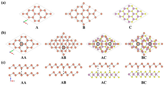
Figure 1.
(Color online) (a) Top view of the antimonene and MoS2 monolayer; (b) top view and (c) side view of the bilayer antimonene and the Sb/MoS2 hetero-bilayer. Sb, Mo and S atoms are represented by red, purple and yellow balls, respectively.
The optimized structural parameters of the bilayer antimonene are shown in Table 1. The lattice constant “a” of the AA and AB stacking is 12.73 Å and 12.28 Å, respectively. Compared to the isolated antimonene, the AA stacking structure is stretched by 4.5% and the AB stacking structure is stretched by 0.8%. The results show that there is a significant difference in the lattice constant between two stacking bilayer antimonene, which is caused by the increased coupling between layers. A shorter interlayer distance was found in the AB stacking bilayer antimonene, indicating that the interlayer interaction of the AB stacking structure is stronger. This can also explain why the amplitude of buckling (∆) of the AA stack is slightly larger than the AB stack. To discuss the relative stabilities of the bilayer systems, all the binding energy () in this paper is defined as:
where and represent the total energies of the isolated monolayers and is the total energy of the heterostructure. The binding energies are given per unit cell. As shown in Table 1, the binding energy of bilayer antimonene and Sb/MoS2 hetero-bilayers are positive. This indicates that the layer stack is an exothermic process; in other words, the two-layer system discussed in this paper can exist stably. In addition, the small binding energy also indicates the weak interaction between the antimonene and MoS2 layers. The binding energy of bilayer antimonene optimized via the PBE-D2 method is 2.275 eV and 3.513 eV for the AA and AB stacking model, respectively (see Table 1), indicating that the interlayer interaction of the AB stacking is stronger than that of the AA stacking.

Table 1.
Geometries and binding energies of antimonene and MoS2 monolayer, antimonene bilayer, Sb/MoS2 hetero-bilayers and Sb/MoS2 superlattice, including the bond length, interlayer distance of stacked layer structure (h) and the amplitude of bucking of the antimonene layers (ΔSb).
In order to better understand the properties of antimonene-based hybrid structures, we also studied the hetero-bilayer (labeled as Sb/MoS2) and superlattice (labeled as Sb/MoS2) composed of antimonene and monolayer MoS2. For hybrid systems, to quantitatively characterize the interlayer interaction, the binding energy between the antimonene and MoS2 sheet was calculated using the adsorption energy formula. is the total energy of the Sb/MoS2 hetero-bilayer and / is the total energy of the isolated Sb sheet or monolayer MoS2. Similar to bilayer antimonene, for hybrid systems, we also considered two representative arrangements of antimonene on monolayer MoS2 (AC and BC). The optimized lattice constant “a” of the Sb/MoS2 hetero-bilayer is 12.67 Å and 12.66 Å, respectively. Judging from the optimized structural parameters and electronic structures of hetero-bilayer Sb/MoS2, there is no big difference between the AC and BC stacking structures (shown in Figure 1). These results indicate that the energetics of antimonene on MoS2 are not sensitive to the stacking models, which is similar to that of previous MoS2-based hybrid systems [29,30,31]. Compared to the corresponding isolated sheet, the Sb layer in the Sb/MoS2 hetero-bilayer is stretched by 3.94% (from 4.06 to 4.22 Å), while the MoS2 layer in the Sb/MoS2 heterogeneous double is compressed by 0.63% (from 3.19 to 3.17 Å).
Figure 2 illustrates the electronic band structures of the bilayer systems. For monolayer antimonene, the maximum valence band (VBM) is located at the high symmetry Γ point, and the conduction band minimum (CBM) is located between the high symmetry point Γ and M. This indicates that the Sb monolayer is an indirect band gap semiconductor with a band gap of 1.25 eV, which is in good agreement with the reported value [21,22,23,24,25]. Moreover, for the MoS2 monolayer (shown in Figure 2b), both VBM and CBM are located between the high symmetry points Γ and M, suggesting that the MoS2 monolayer is a direct band gap semiconductor. The electronic band structures of bilayer antimonene with two different stacking models are shown in Figure 2c,d. We can see that the VBM of the AA stacked is located between the high symmetry points Γ and K, and the CBM is located at the high symmetry point Γ from Figure 2c. However, the CBM and VBM of the AB stacked are both located between the high symmetry points Γ and M. Therefore, the bilayer antimonene is an indirect band gap semiconductor with a band gap of 0.36 eV (AA stacking) and 0.25 eV (AB stacking). The band gap value of the bilayer antimonene is reduced compared to the Sb monolayer, which is consistent with other van der Waals layered structures [22,23,24,25]. Compared to the Sb monolayer, the band gap value of the bilayer antimonene is significantly sunken regardless of the model stack. This facilitates the charge transfer between layers and realizes the application of Sb in photovoltaic cells.
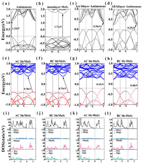
Figure 2.
Band structures of (a) antimonene, (b) MoS2 monolayer, (c) AA bilayer antimonene, (d) AB bilayer antimonene, (e) AC Sb/MoS2 hetero-bilayer, (f) BC Sb/MoS2 hetero-bilayer, (g) AC Sb/MoS2 superlattice and (h) BC Sb/MoS2 superlattice. The density of states of (i) AC Sb/MoS2 hetero-bilayer, (j) BC Sb/MoS2 hetero-bilayer, (k) AC Sb/MoS2 superlattice and (l) BC Sb/MoS2 superlattice. The black dotted line indicates the Fermi level.
The projected band structures of hetero-bilayer Sb/MoS2 are shown in Figure 2e,f, the red and blue circles representing the contributions of Sb and MoS2 to the eigenstate, respectively. We can clearly see that the band structure of the Sb/MoS2 heterostructure is a simple superposition of the components. There is a simple coupling effect between Sb and MoS2 layers so that the electronic structure of Sb and MoS2 monolayer can be preserved. Both for AC and for BC stacking, the CBM and VBM are located between the high symmetry points Γ and M, indicating that the Sb/MoS2 hetero-bilayer is an indirect band gap semiconductor. In addition, the VBM of the Sb/MoS2 heterostructure is mainly distributed from Sb, while the CBM is localized in MoS2. Therefore, the Sb/MoS2 is a type-II hetero-bilayer structure. In the Sb/MoS2 type-II energy band alignment, MoS2 acts as an electron acceptor and Sb acts as an electron donor. According to the density of states (DOS) of the Sb/MoS2 hetero-bilayer shown in Figure 2i,j, the energy band near the Fermi level originates from the electron hybridization of the p orbital of Sb and the d orbital of Mo. Under the action of the VBM shift, the electrons in Sb can be easily transferred to the conduction band of the MoS2 layer. At the same time, the holes of the MoS2 layer can be easily transferred to the valence band of the Sb layer. Due to the electron and hole transfer, the electron–hole pairs of the Sb/MoS2 heterostructure decrease. This will effectively extend the life of the optoelectronics, thereby improving the performance of electronic and optoelectronic devices.
The band structures of Sb/MoS2 superlattice are shown in Figure 2g,h. The superlattices with two different stackings are all shown to be direct band gap semiconductors. Compared with the hetero-bilayer Sb/MoS2, the CBM of the Sb/MoS2 superlattice is still all contributed by MoS2, while the VBM is occupied by Sb and MoS2. The total and partial DOS of Sb/MoS2 superlattice are shown in Figure 2k,l. Within each monolayer of MoS2, there is strong hybridization between the Mo-d orbitals and the S-s orbitals, and the Mo-S bond could preserve its covalent bonding. Compared with the Sb/MoS2 hetero-bilayer (Figure 2i,j), we can clearly see that the contribution of antimonene in the valence band decreases, and the conduction band moves close to the Fermi level, leading to a decreased band gap in the Sb/MoS2 superlattice. By controlling the number of layers in heterostructures, antimonene-based hybrid structures could realize a transformation from a type-I semiconductor to a type-II semiconductor. The results of this work provide a promising way to design applications in future antimonene-based nanodevices with controlled band gaps.
In order to better study the bonding nature and charge transfer of hybrid systems, we calculated the difference in charge density of planes perpendicular to the atomic layers and passing through Mo-S and Sb-Sb bonds (shown in Figure 3). The differential charge density () here is defined as:
where represents the total charge density of the heterostructure system and is the superposition of atomic charge densities. The red solid line ( > 0) and the blue dashed line ( < 0) indicate the increase and decrease in the electron density after bonding, respectively. All the charge densities here are calculated using the same supercell for the heterostructures. As shown in Figure 3, within each atomic layer, the atomic bonding of Mo-S and Sb–Sb could preserve their covalent bonding, indicating that the interactions within each 2D sheet in heterostructures are not affected significantly by the introduction of foreign 2D materials. However, the weak interaction between layers will lead to a simple coupling effect between Sb and MoS2 layers. To clarify the specific reasons, the Bader analysis for the heterostructures was performed to calculate the charge transfer between the antimonene and MoS2 monolayer. According to the data in Table 2, we found that electrons are transferred from the Sb layer to the neighboring MoS2 layer (at the junction of MoS2 and Sb layers). However, the amount of charge transfer is very small (less than one electron). This charge is newly distributed after the formation of the Sb/MoS2 heterostructures, which hinders the recombination of electron–hole pairs and balances the system.
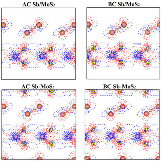
Figure 3.
Deformation charge density ( for hybrid systems of planes perpendicular to the atomic layers and passing through Mo-S and Sb-Sb bonds. The red solid line and the blue dashed line indicate < 0 and < 0, respectively.
Table 2.
Bader analysis for the heterostructures.
Compared to the isolated antimonene and MoS2 monolayer, the Sb and MoS2 layers in the hetero-bilayer have to be compressed or stretched to match each other. Thus, in order to get further insight into the effect of the in-plane biaxial strain on the hetero-bilayer systems, we systematically studied the electronic band structures and differential charge density of compressed (from −1% to −8%) and stretched (from 1% to 4%) Sb/MoS2 hetero-bilayers. The in-plane biaxial strain (ε) is defined as:
where a and a0 are the strained and unstrained lattice constants, respectively. The electronic band structures of the Sb/ MoS2 hetero-bilayer under different strains are shown in Figure 4, in which the band contribution from the antimonene and MoS2 monolayer are shown with blue and red dots, respectively. The band structure of the unstrained Sb/MoS2 hetero-bilayer is also depicted in the middle of Figure 4 for comparison. For Sb/MoS2 hetero-bilayers, the compressed (less than −8%) or stretched (less than 4%) systems are still semiconductors with indirect band gaps. However, it can be seen that the value of band gaps can be varied by compressing or stretching the lattice constants (shown in Table 3). A maximum band gap of 1.00 eV appears at the Sb/MoS2 hetero-bilayer with a compressed strain of −2%. For stretched Sb/MoS2 hetero-bilayers, the magnitude of band gaps decreases monotonically with an increase in lattice parameters. The size of the strain-induced band gap of Sb/MoS2 hetero-bilayers is in the range of 0.10~1.00 eV. As the lattice constant is decreased, the band moves toward the deeper energy level. When a compressive strain of −8% is applied, the Sb/MoS2 hetero-bilayer is metallic. Hence, through compressing or stretching, the hetero-bilayers realize the transformation from a metal to an indirect band gap semiconductor.
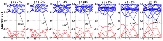
Figure 4.
The electronic band structures of the Sb/MoS2 hetero-bilayer under different in-plane biaxial strain: (a) ε = −3%, (b) ε = −2%, (c) ε = −1%, (d) ε = 0%, (e) ε = 1%, (f) ε = 2%, (g) ε = 3%. Contribution from antimonene and MoS2 monolayer to the band structures of the bilayers are shown with red and blue circle dots, respectively. The Fermi level is set to 0 eV.
Table 3.
Band gaps of compressed/stretched Sb/MoS2 hetero-bilayer.
4. Conclusions
In summary, the electronic structures and properties of hybrid systems composed of antimonene and monolayer MoS2 were studied through density functional theory calculations. The Sb/MoS2 hetero-bilayer and Sb/MoS2 superlattice are both type-II band alignment, which implies the spatial separation of photogenerated electron–hole pairs. The Sb/MoS2 hetero-bilayers are indirect band gap semiconductors, while the Sb/MoS2 superlattices were shown to be direct band gap semiconductors with decreased band gaps. Due to the weak van der Waals interlayer interactions between layers, the electronic properties of each component can be preserved in the hybrid systems. In addition, the band gap of the Sb/MoS2 hetero-bilayer can be effectively controlled by the biaxial strain, which improves its electronic performance in nanodevices. Our results show that antimonene-based hybrid systems are promising candidates for photovoltaic devices.
Author Contributions
Formal analysis, X.L.; funding acquisition, T.H.; investigation, C.Z.; project administration, X.L.; supervision, X.L.; writing—original draft, C.Z.; writing—review and editing, X.L. All authors have read and agreed to the published version of the manuscript.
Funding
This work is supported by the Fundamental Research Funds for the Central Universities, China under grant No. 2412019FZ037.
Conflicts of Interest
The authors declare no conflict of interest.
References
- Xie, C.; Mak, C.H.; Tao, X.M.; Yan, F. Photodetectors Based on Dwo-Dimensional Layered Materials Beyond Graphene. Adv. Funct. Mater. 2017, 27, 1603886. [Google Scholar] [CrossRef]
- Wu, J.B.; Lin, M.L.; Cong, X.; Liu, H.N.; Tan, P.H. Raman Spectroscopy of Graphene-Based Materials and Its Applications in Related Devices. Chem. Soc. Rev. 2018, 47, 1822–1873. [Google Scholar] [CrossRef] [PubMed]
- Yu, X.W.; Cheng, H.H.; Zhang, M.; Zhao, Y.; Qu, L.T.; Shi, G.Q. Graphene-Based Smart Materials. Nat. Rev. Mater. 2017, 2, 17046. [Google Scholar] [CrossRef]
- Lu, X.B.; Stepanov, P.; Yang, W.; Xie, M.; Aamir, M.A.; Das, I.; Urgell, C.; Watanabe, K.; Taniguchi, T.; Zhang, G.; et al. Superconductors, Orbital Magnets and Correlated States in Magic-Angle Bilayer Graphene. Nature 2019, 574, 653–657. [Google Scholar] [CrossRef]
- Abraham, J.; Vasu, K.S.; Williams, C.D.; Gopinadhan, K.; Su, Y.; Cherian, C.; Dix, J.; Prestat, E.; Haigh, S.J.; Grigorieva, I.V.; et al. Tuneable Sieving of Ions Using Graphene Oxide Membranes. Nat. Nanotechnol. 2017, 12, 546–550. [Google Scholar] [CrossRef]
- Mo, R.W.; Rooney, D.; Sun, K.; Yang, H.Y. 3D Nitrogen-Doped Graphene Foam with Encapsulated Germanium/Nitrogen-Doped Graphene Yolk-Shell Nanoarchitecture for High-Performance Flexible Li-Ion Battery. Nat. Commun. 2017, 8, 13949. [Google Scholar] [CrossRef]
- Li, X.L.; Zhi, L.J. Graphene Hybridization for Energy Storage Applications. Chem. Soc. Rev. 2018, 47, 3189–3216. [Google Scholar] [CrossRef]
- Lee, I.H.; Yoo, D.; Avouris, P.; Low, T.; Oh, S.H. Graphene Acoustic Plasmon Resonator for Ultrasensitive Infrared Spectroscopy. Nat. Nanotech. 2019, 14, 313–319. [Google Scholar] [CrossRef]
- Geng, P.B.; Zheng, S.S.; Tang, H.; Zhu, R.M.; Zheng, L.; Cao, S.; Xue, H.G.; Pang, H. Transition Metal Sulfides Based on Graphene for Electrochemical Energy Storage. Adv. Energy Mater. 2018, 8, 1703259. [Google Scholar] [CrossRef]
- Xu, Y.; Zhang, C.L.; Zhou, M.; Fu, Q.; Zhao, C.X.; Wu, M.H.; Lei, Y. Highly Nitrogen Doped Carbon Nanofibers with Superior Rate Capability and Cyclability for Potassium Ion Batteries. Nat. Commun. 2018, 9, 1720. [Google Scholar] [CrossRef]
- Ma, J.; Liu, C.T. Using Negative Thermal Expansion Effect to Grow Spiny NiS/C Architecture and Its Application in Sodium-Ion Batteries. J. Alloys Compd. 2020, 829, 154572. [Google Scholar] [CrossRef]
- Cai, Z.X.; Su, L.; Wang, H.J.; Niu, M.; Gao, H.F.; Lu, D.; Li, M.Z. Hydrophobic SiC@C Nanowire Foam with Broad-Band and Mechanically Controlled Electromagnetic Wave Absorption. ACS Appl. Mater. Interfaces 2020, 12, 8555–8562. [Google Scholar] [CrossRef] [PubMed]
- Wong, K.L.; Chuan, M.W.; Hamzah, A.; Rusli, S.; Alias, N.; Sultan, M.S.; Lim, C.S.; Tan, M.L.T. Electronic Properties of Graphene Nanoribbons with Line-Edge Roughness Doped with Nitrogen and Boron. Physica E 2020, 117, 13841. [Google Scholar] [CrossRef]
- Tang, S.B.; Wu, W.H.; Xie, X.J.; Li, X.K.; Gu, J.J. Band Gap Opening of Bilayer Graphene by Graphene Oxide Support Doping. RSC Adv. 2017, 7, 9862–9871. [Google Scholar] [CrossRef]
- Yang, J.; Tang, L.S.; Bao, R.Y.; Bai, L.; Liu, Z.Y.; Xie, B.H.; Yang, M.B.; Yang, W. Hybrid Network Structure of Boron Bitride and Graphene Oxide in Shape-Stabilized Composite Phase Change Materials with Enhanced Thermal Conductivity and Light-to-Electric Energy Conversion Capability. Sol. Energy Mater. Sol. Cells. 2018, 174, 56–64. [Google Scholar] [CrossRef]
- Ji, M.X.; Xia, J.X.; Di, J.; Liu, Y.L.; Chen, R.; Chen, Z.G.; Yin, S.; Li, H.M. Graphene-Like Boron Nitride Induced Accelerated Charge Transfer for Boosting the Photocatalytic Behavior of Bi4O5I2 Towards Bisphenol a Removal. Chem. Eng. J. 2018, 331, 355–363. [Google Scholar] [CrossRef]
- Li, Q.; Huo, C.R.; Yi, K.; Zhou, L.L.; Su, L.; Hou, X.M. Preparation of Flake Hexagonal BN and Its Application in Electrochemical Detection of Ascorbic Acid, Dopamine and Uric Acid. Sens. Actuators B 2018, 260, 346–356. [Google Scholar] [CrossRef]
- Zhao, J.; Li, N.; Yu, H.; Wei, Z.; Liao, M.Z.; Chen, P.; Wang, S.P.; Shi, D.X.; Sun, Q.J.; Zhang, G.Y. Highly Sensitive MoS2 Humidity Sensors Array for Noncontact Sensation. Adv. Mater. 2017, 29, 1702076. [Google Scholar] [CrossRef]
- Liu, W.J.; Zhu, Y.N.; Liu, M.L.; Wen, B.; Fang, S.B.; Teng, H.; Lei, M.; Liu, L.M.; Wei, Z.Y. Optical Properties and Applications for MoS2-Sb2Te3-MoS2 Heterostructure Materials. Photonics Res. 2018, 6, 220–227. [Google Scholar] [CrossRef]
- Sangeetha, M.; Madhan, D. Ultra Sensitive Molybdenum Disulfide (MoS2)/graphene Based Hybrid Sensor for The Detection of NO2 and Formaldehyde Gases by Fiber Optic Clad Modified Method. Opt. Laser Technol. 2020, 127, 106193. [Google Scholar] [CrossRef]
- Ares, P.; Aguilar-Galindo, D.; Rodriguez-San-Miguel, D.; Aldave, D.A.; Diaz-Tendero, S.; Alcami, M.; Martin, F.; Gomez-Herrero, J.; Zamora, F. Mechanical Isolation of Highly Stable Antimonene Under Ambient Conditions. Adv. Mater. 2016, 28, 6332–6336. [Google Scholar] [CrossRef] [PubMed]
- Pumera, M.; Sofer, Z. 2D Monoelemental Arsenene, Antimonene, and Bismuthene: Beyond Black Phosphorus. Adv. Mater. 2017, 29, 1605299. [Google Scholar] [CrossRef] [PubMed]
- Xie, M.Q.; Zhang, S.L.; Cai, B.; Gu, Y.; Liu, X.H.; Kan, E.J.; Zeng, H.B. Van der Waals Bilayer Antimonene: A Promising Thermophotovoltaic Cell Material With 31% Energy Conversion Efficiency. Nano Energy 2017, 38, 561–568. [Google Scholar] [CrossRef]
- Wang, X.X.; Tang, C.M.; Zhou, X.F.; Zhu, W.H.; Fu, L. The Good Performance of Bilayer β-Antimoneneas an Anode Material for the Li-ion Battery Study. Appl. Surf. Sci. 2019, 495, 143549. [Google Scholar] [CrossRef]
- Zhang, J.J.; Zhang, Y.; Dong, S. Protective Layer Enhanced Stability and Superconductivity of Tailored Antimonene Bilayer. Phys. Rev. Mater. 2018, 2, 126004. [Google Scholar] [CrossRef]
- Alarawi, A.; Ramalingam, V.; Fu, H.C.; Purushothaman, V.; Yang, R.; He, J.H. Enhanced Photoelectrochemical Hydrogen Production Efficiency of MoS2-Si Heterojunction. Opt. Express 2019, 27, A352–A363. [Google Scholar] [CrossRef] [PubMed]
- Qiao, S.; Cong, R.D.; Liu, J.H.; Liang, B.L.; Fu, G.S.; Yu, W.; Ren, K.L.; Wang, S.F.; Pan, C.F. A Vertically Layered MoS2/Si Heterojunction for an Ultrahigh and Ultrafast Photoresponse Photodetector. J. Mater. Chem. C 2018, 6, 3233–3239. [Google Scholar] [CrossRef]
- Son, S.B.; Kim, Y.; Cho, B.; Choi, C.J.; Hong, W.K. Temperature-Dependent Electronic Charge Transport Characteristics at MoS2/p-type Ge heterojunctions. J. Alloys Compd. 2018, 757, 221–227. [Google Scholar] [CrossRef]
- Li, X.D.; Yu, S.; Wu, S.Q.; Zhou, S.; Zhu, Z.Z. Structural and Electronic Properties of Germanene/MoS2 Monolayer and Silicene/MoS2 Monolayer Superlattices. Nanoscale Res. Lett. 2014, 9, 110. [Google Scholar] [CrossRef]
- Wan, W.; Li, X.D.; Li, X.T.; Xu, B.B.; Zhan, L.J.; Zhao, Z.J.; Zhang, P.C.; Wu, S.Q.; Zhu, Z.Z.; Huang, H.; et al. Interlayer Coupling of a Direct Van der Waals Epitaxial MoS2/graphene Heterostructure. RSC Adv. 2016, 6, 323–330. [Google Scholar] [CrossRef]
- Li, X.D.; Yu, S.; Wu, S.Q.; Wen, Y.H.; Zhou, S.; Zhu, Z.Z. Structural and Electronic Properties of Superlattice Composed of Graphene and Monolayer MoS2. J. Phys. Chem. C 2013, 117, 15347–15353. [Google Scholar] [CrossRef]
- Han, J.K.; Du, G.L.; Gao, W.W.; Bai, H. An Anisotropically High Thermal Conductive Boron Nitride/Epoxy Composite Based on Nacre-Mimetic 3D Network. Adv. Funct. Mater. 2019, 29, 1900412. [Google Scholar] [CrossRef]
- Chittari, B.L.; Chen, G.R.; Zhang, Y.B.; Wang, F.; Jung, J. Gate-Tunable Topological Flat Bands in Trilayer Graphene-Boron Nitride Moire Superlattices. Phys. Rev. Lett. 2019, 122, 016401. [Google Scholar] [CrossRef] [PubMed]
- Jiang, Y.Y.; Lin, X.; Low, T.; Zhang, B.L.; Chen, H.S. Group-Velocity-Controlled and Gate-Tunable Directional Excitation of Polaritons in Graphene-boron Nitride Heterostructures. Laser Photonics Rev. 2018, 12, 1800049. [Google Scholar] [CrossRef]
- Laturia, A.; Van de Put, M.L.; Vandenberghe, W.G. Dielectric Properties of Hexagonal Boron Nitride and Transition Metal Dichalcogenides: From Monolayer to Bulk. NPJ 2D Mater. Appl. 2018, 2, 6. [Google Scholar] [CrossRef]
- Pham, K.D.; Hieu, N.N.; Bui, L.M.; Phuc, H.V.; Hoi, B.D.; Tu, L.T.N.; Bach, L.G.; Ilyasov, V.V.; Amin, B.; Idress, M.; et al. Vertical Strain and Electric Field Tunable Electronic Properties of Type-II Band Alignment C2N/InSe Van der Waals Heterostructure. Chem. Phys. Leet. 2019, 716, 155–161. [Google Scholar] [CrossRef]
- You, B.Q.; Wang, X.C.; Zheng, Z.D.; Mi, W.B. Black Phosphorene/Monolayer Transition-Metal Dichalcogenides as two Dimensional Van der Waals Heterostructures: A First-Principles Study. Phys. Chem. Chem. Phys. 2016, 18, 7381–7388. [Google Scholar] [CrossRef]
- Zhang, F.; Li, W.; Dai, X.Q. Effects of Interlayer Coupling on the Electronic Structures of Antimonene/Graphene Wan der Waals Heterostructures. Superlattices Microstruct. 2016, 100, 826–832. [Google Scholar] [CrossRef]
- Shen, N.F.; Yang, X.D.; Wang, X.X.; Wang, G.H.; Wan, J.G. Two-Dimensional Van der Waals Heterostructure of Indium Selenide/Antimonene: Efficient Carrier Separation. Chem. Phys. Lett. 2019, 727, 50–54. [Google Scholar] [CrossRef]
- Sham, L.J.; Schlüter, M. Density-Functional Theory of the Energy Gap. Phys. Rev. Lett. 1983, 51, 1888–1891. [Google Scholar] [CrossRef]
- Kresse, G.; Furthmüller, J. Efficient Iterative Schemes for Ab Initio Total-Energy Calculations Using a Plane-Wave Basis Set. Phys. Rev. B 1996, 54, 11169–11186. [Google Scholar] [CrossRef] [PubMed]
- Kresse, G.; Furthmüller, J. Efficiency of Ab-Initio Total Energy Calculations for Metals and Semiconductors Using a Plane-Wave Basis Set. Comput. Mater. Sci. 1996, 6, 15–50. [Google Scholar] [CrossRef]
- Perdew, P.J.; Burke, K.; Ernzerhof, M. Generalized Gradient Approximation Made Simple. Phys. Rev. Lett. 1996, 77, 3865–3868. [Google Scholar] [CrossRef] [PubMed]
- Perdew, P.J.; Zunger, A. Self-Interaction Correction to Density-Functional Approximations for Many-Electron Systems. Phys. Rev. B 1981, 23, 5048–5079. [Google Scholar] [CrossRef]
- Grimme, S. Semiempirical GGA-Dype Density Functional Constructed with A Long-Range Dispersion Correction. J. Comput. Chem. 2006, 27, 1787–1799. [Google Scholar] [CrossRef] [PubMed]
- Chadi, D.J. Special Points for Brillouin-Zone Integrations. Phys. Rev. B 1977, 16, 1746–1747. [Google Scholar] [CrossRef]
- Ramírez, R.; Böhm, M.C. Simple Geometric Generation of Special Points in Brillouin-Zone Integrations. Two-Dimensional Bravais Lattices. Int. J. Quantum Chem. 1986, 30, 391–411. [Google Scholar] [CrossRef]
- Chen, B.; Meng, Y.H.; Sha, J.W.; Zhong, C.; Hu, W.B.; Zhao, N.Q. Preparation of MoS2/TiO2 Based Nanocomposites for Photocatalysis and Rechargeable Batteries: Progress, Challenges, and Perspective. Nanoscale 2017, 10, 34–68. [Google Scholar] [CrossRef]
- Wang, S.; Ren, C.D.; Tian, H.Y.; Yu, J.; Sun, M.L. MoS2/ZnO Van der Waals Heterostructure as A High-Efficiency Water Splitting Photocatalyst: A First-Principles Study. Phys. Chem. Chem. Phys. 2018, 20, 13394–13399. [Google Scholar] [CrossRef]
- Wu, X.; Shao, Y.; Liu, H.; Feng, Z.L.; Wang, Y.L.; Sun, J.T.; Liu, C.; Wang, J.Q.; Liu, Z.L.; Zhu, S.Y.; et al. Epitaxial Growth and Air-Stability of Monolayer Antimonene on PdTe2. Adv. Mater. 2017, 29, 1605407. [Google Scholar] [CrossRef]
- Shao, Y.; LIiu, Z.L.; Cheng, C.; Wu, X.; Liu, H.; Liu, C.; Wang, J.O.; Zhu, S.Y.; Wang, Y.Q.; Shi, D.X.; et al. Epitaxial Growth of Flat Antimonene Monolayer: A New Honeycomb Analogue of Graphene. Nano Lett. 2018, 18, 2133–2139. [Google Scholar] [CrossRef] [PubMed]
- Ares, P.; Palacios, J.J.; Abellan, G.; Gomez-Herrero, J.; Zamora, F. Recent Progress on Antimonene: A New Bidimensional Material. Adv. Mater. 2017, 30, 1703771. [Google Scholar] [CrossRef] [PubMed]
- Chen, X.P.; Meng, R.S.; Jiang, J.K.; Liang, Q.H.; Yang, Q.; Tan, C.J.; Sun, X.; Zhang, S.L.; Ren, T.L. Electronic Structure and Optical Properties of Graphene/Stanene Heterobilayer. Phys. Chem. Chem. Phys. 2016, 18, 16302–16309. [Google Scholar] [CrossRef] [PubMed]
- Águila, E.J.C.; Palacios, P.; Conesa, C.J.; Arriaga, J.; Wahnón, P. Electronic Band Alignment at CuGaS2 Chalcopyrite Interfaces. Comput. Mater. Sci. 2016, 121, 79–85. [Google Scholar] [CrossRef]
- Si, F.J.; Hu, W.; Tang, F.L.; Cheng, Y.W.; Xue, H.T. Electronic and Optical Properties of the Wurtzite-ZnO/CH3NH3PbI3 Interface: First-Principles Calculations. J. Mater. Sci. 2017, 52, 13841–13851. [Google Scholar] [CrossRef]
Publisher’s Note: MDPI stays neutral with regard to jurisdictional claims in published maps and institutional affiliations. |
© 2020 by the authors. Licensee MDPI, Basel, Switzerland. This article is an open access article distributed under the terms and conditions of the Creative Commons Attribution (CC BY) license (http://creativecommons.org/licenses/by/4.0/).