Article

Synthesis and Characterization of CuIn1−xGaxSe2 Semiconductor Nanocrystals

1
Department of Physics, National Changhua University of Education, Changhua 50007, Taiwan
2
Department of Electronic Engineering, National Changhua University of Education, Changhua 50074, Taiwan
*
Author to whom correspondence should be addressed.
Nanomaterials 2020, 10(10), 2066; https://doi.org/10.3390/nano10102066
Submission received: 11 August 2020 / Revised: 22 September 2020 / Accepted: 11 October 2020 / Published: 19 October 2020
(This article belongs to the Special Issue Nanocrystals: Synthesis, Properties and Applications)

Abstract

:
In this paper, the synthesis and characterization of CuIn1−xGaxSe2 (0 ≤ x ≤ 1) nanocrystals are reported with the influences of x value on the structural, morphological, and optical properties of the nanocrystals. The X-ray diffraction (XRD) results showed that the nanocrystals were of chalcopyrite structure with particle size in the range of 11.5–17.4 nm. Their lattice constants decreased with increasing Ga content. Thus, the x value of the CuIn1−xGaxSe2 nanocrystals was estimated by Vegard’s law. Transmission electron microscopy (TEM) analysis revealed that the average particle size of the nanocrystals agreed with the results of XRD. Well-defined lattice fringes were shown in the TEM images. An analysis of the absorption spectra indicated that the band gap energy of these CuIn1−xGaxSe2 nanocrystals was tuned from 1.11 to 1.72 eV by varying the x value from 0 to 1. The Raman spectra indicated that the A1 optical vibrational mode of the nanocrystals gradually shifted to higher wavenumber with increasing x value. A simple theoretical equation for the A1 mode frequency was proposed. The plot of this equation showed the same trend as the experimental data.

1. Introduction

In recent years, due to issues of global warming, the exhaustion of traditional and nonrenewable energy sources, and the goal of gradually reducing nuclear power generation, the demand for clean, safe, and renewable energy around the world has increased significantly. The research and development of photovoltaic devices have attracted great interest and attention.
The earliest photovoltaic devices were made of crystalline silicon, which is currently the main material for the mass production of solar cell modules. However, due to high production costs, many researchers have turned to other photovoltaic materials in order to replace crystalline silicon. Among them, CuIn1−xGaxSe2 has received extensive attention.
CuIn1−xGaxSe2 is a quaternary semiconductor material belonging to the family of I–III–VI2 compounds [1]; it has a tetragonal chalcopyrite structure. CuIn1−xGaxSe2 has good optical properties, such as intrinsic high optical absorption coefficient (α ≈ 105/cm), wide absorption range, good radiation stability [2,3,4,5], and a direct bandgap which is adjustable by changing the composition ratio of In to Ga. For this reason, it is regarded as an excellent absorber layer material for thin-film solar cell applications [6,7]. A recent report indicated that the conversion efficiency of CuIn1−xGaxSe2 solar cells has reached 22.6% [8]. Additionally, CuIn1−xGaxSe2 could be a promising material for other optoelectronic applications because its composition tunability opens another parameter with which to achieve specific properties and performance [9].
Generally, the absorber layers of solar cells are manufactured by vacuum-based processes, which have the disadvantages of complicated procedures, problems in scale-up, and high production costs. A promising approach for improvement is using semiconducting nanocrystals in the manufacturing processes of solar energy harvesting devices [10,11,12,13,14]. Nanocrystal-based printing/coating technology for the absorber layers of photovoltaic devices can not only reduce production costs, but also achieve high efficiency [15,16]. Research results have shown that CuIn1−xGaxSe2 nanocrystals are a good absorber layer material for thin-film solar cell applications [4,5,17].
There are various methods for manufacturing CuIn1−xGaxSe2 nanocrystals, such as hot injection synthesis [5,18], the solvothermal route [4], thermal decomposition [19,20,21], the modified polyol route [22], and the mechanochemical process [23]. Cui and co-workers synthesized CuIn1−xGaxSe2 nanocrystals by heating metal chlorides in a selenium solution containing oleylamine and glycerol [24]. Recently, two-step procedures, which include a low temperature (110 °C) nucleation stage lasting 24 h followed by a growth step at higher temperature (240 °C) lasting 1 h, to synthesize CuIn1−xGaxSe2 nanocrystals with sphalerite or wurtzite phase were reported [25]. In this paper, we report the synthesis of CuIn1−xGaxSe2 nanocrystals over the entire nominal composition range (0 ≤ x ≤ 1) by a solution-based method [26]. Due to the low reaction temperature and short reaction time, this method is one of the simplest synthesis methods for manufacturing CuIn1−xGaxSe2 nanocrystals, and is practical for mass production. In addition, this method has the potential to be environmentally friendly and reduce costs, as there is no need for toxic gases, high vacuum or high temperature facilities.
In this study, the band gap energy of the CuIn1−xGaxSe2 nanocrystals was tuned by varying the x value. The influences of x value on the structural, morphological, and optical properties of the nanocrystals were studied. The nanocrystals could form colloidal suspensions that are paving the way for the fabrication of photovoltaic devices.

2. Materials and Methods

To synthesize CuIn1−xGaxSe2 nanocrystals over the entire nominal composition range, a useful solution-based method was developed [26]. The nominal x values were 0, 0.125, 0.25, 0.375, 0.5, 0.625, 0.75, 0.875, and 1. In a typical preparation procedure, 1 mmol (0.2618 g) of copper(II) acetylacetonate, (1–x) mmol (0.4121(1–x) g) of indium(III) acetylacetonate, x mmol gallium(III) acetylacetonate (0.3671x g), and 3.5 mmol (1.3532 g) of trioctylphosphine oxide were added to a four-neck, round bottom flask containing 10 mL of oleylamine. The mixture was magnetically stirred at room temperature for 30 min and then heated to 150 °C. Afterwards, 2 mmol (0.1579 g) of elemental selenium powder was added to the solution with continuous stirring. The reaction solution was then heated to 230 °C and maintained at this temperature for 30 min with stirring, and then cooled to room temperature. During the synthesis procedure, the reaction was performed under a nitrogen atmosphere. Next, a mixture of 25 mL of hexane and 25 mL of ethanol was added to the solution. The precipitates of the crude solution were collected by centrifugation at 7000 rpm for 15 min. Finally, the precipitated nanocrystals were dissolved into a suitable amount of chloroform and then centrifuged at 7000 rpm for 15 min. This process was repeated two times to obtain high-purity nanocrystals.
The structural properties of the CuIn1−xGaxSe2 nanocrystals were analyzed by X-ray diffraction (XRD) using a Shimadzu XRD-6000 (Kyoto, Japan) diffractometer equipped with Fe Kα radiation. Transmission electron microscope (TEM) images of the nanocrystals were taken using a JEOL JEM-2010 (Tokyo, Japan) transmission electron microscope. For absorption measurements, a 1/4 m monochromator (MKS, Irvine, CA, USA) equipped with a 130 W halogen lamp was used to provide monochromatic light in a photon energy range from 0.9 to 1.8 eV. The continuous light coming from the monochromator was modulated into an alternate light at a frequency of 200 Hz through a mechanical chopper. A silicon photo detector (Thorlabs, Newton, NJ, USA) and an InGaAs photo detector (Thorlabs, Newton, NJ, USA) with an amplifier were placed on the back of the sample to detect the intensity of the transmitting light. The output signal of the detector was recorded by a dual phase lock-in amplifier (Ametek, Berwyn, PA, USA) to suppress noise signals. Raman analyses were performed using a Dongwoo Ramboss Micro Raman (Gwangju-Si, Korea) system with a solid state laser source with an excitation wavelength of 532 nm.

3. Results and Discussion

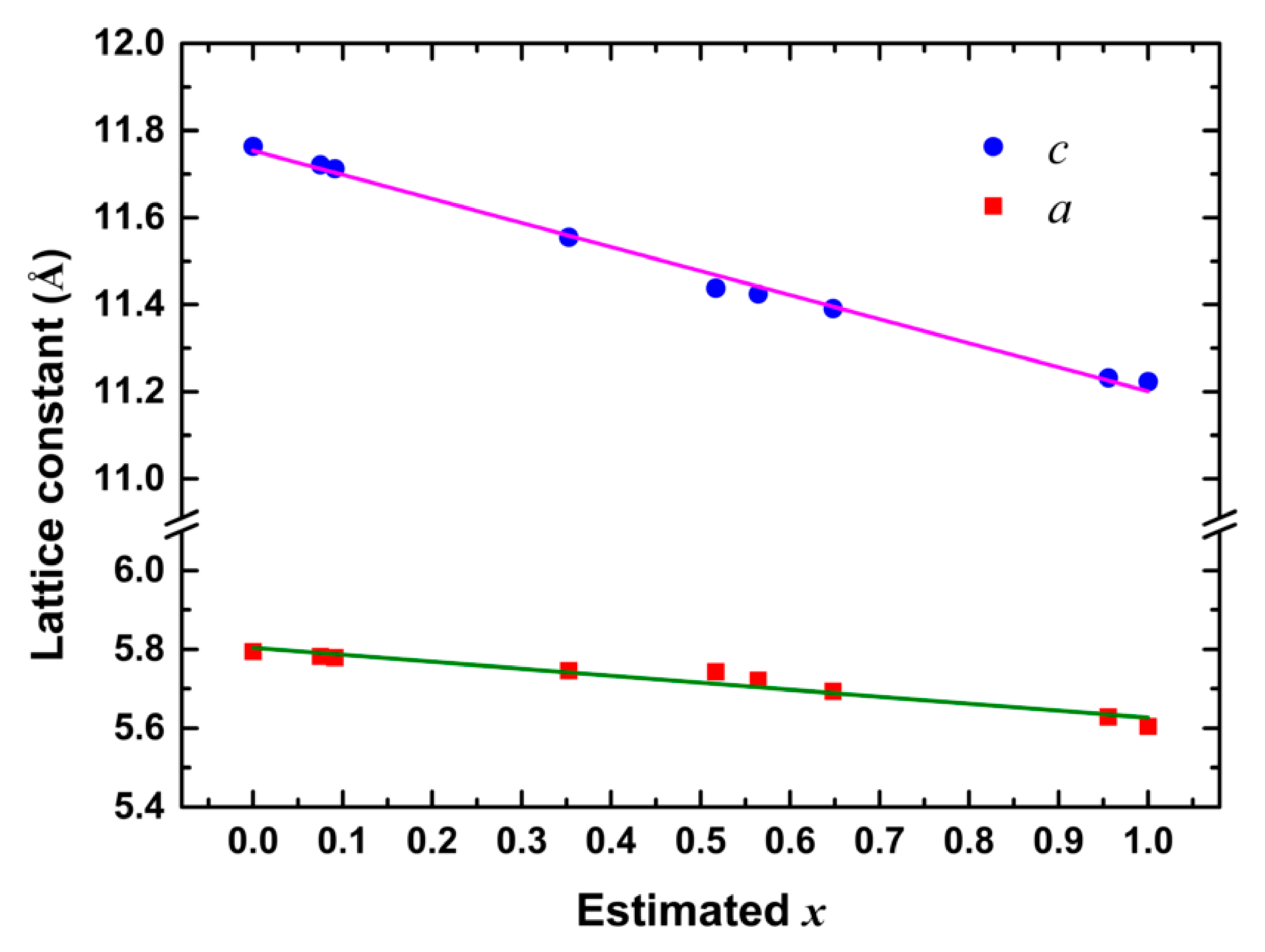
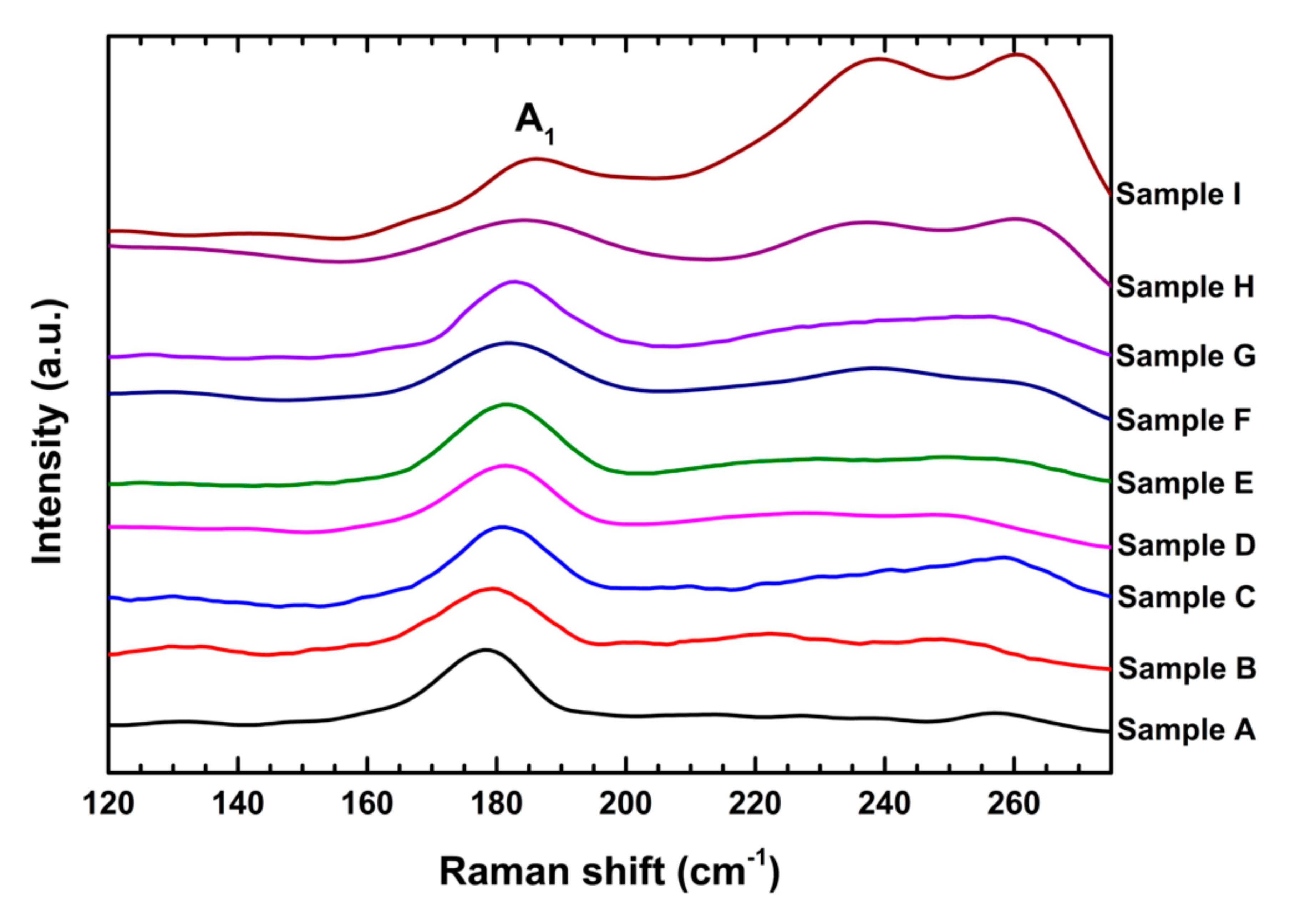
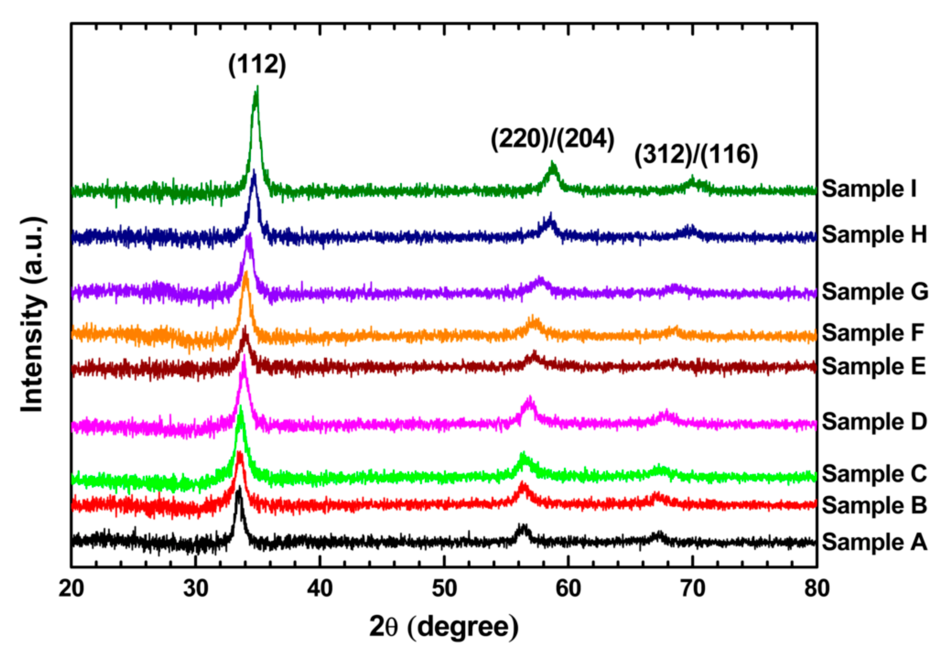
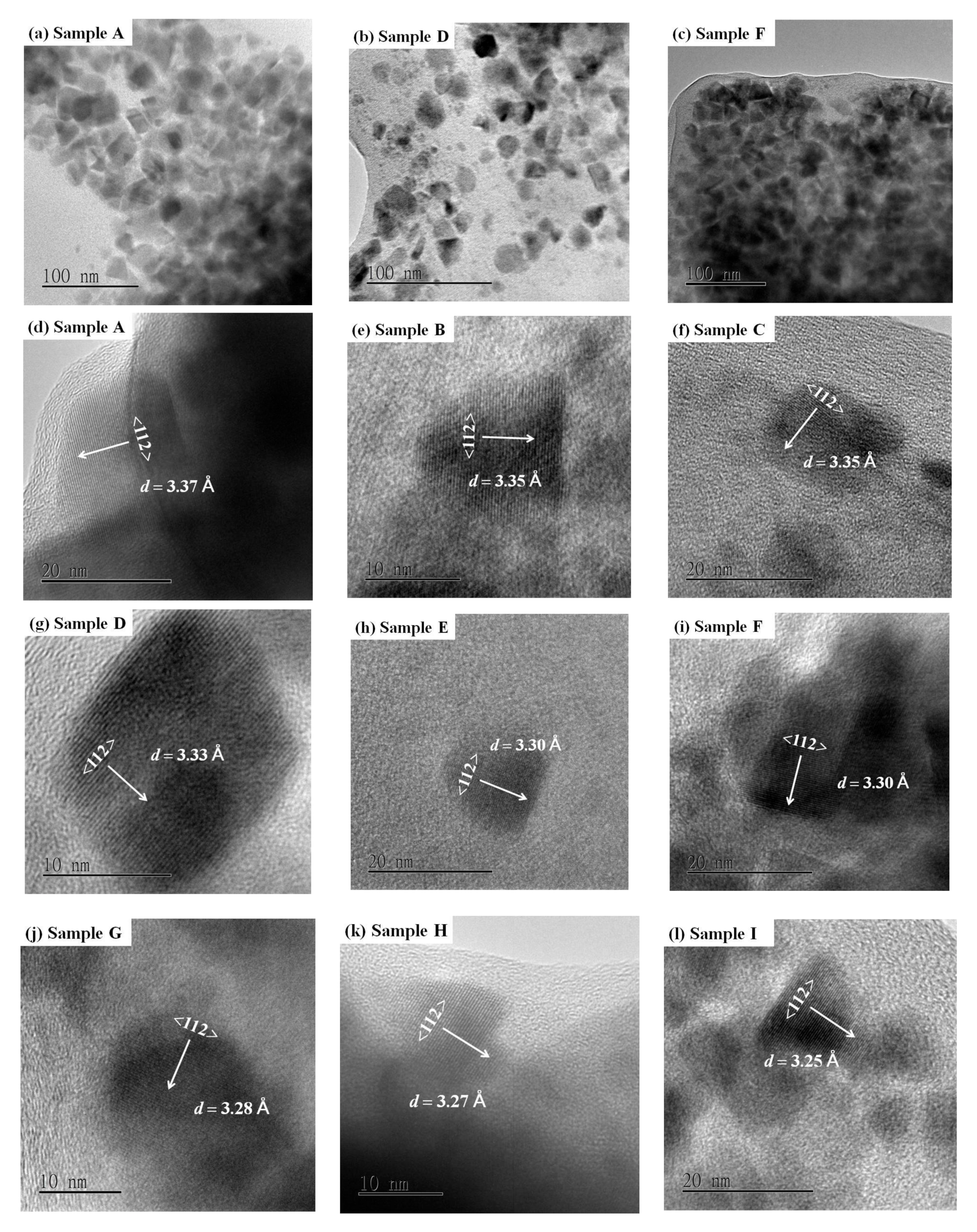
3.1. Structural Properties

Figure 1 shows the XRD patterns of the CuIn1−xGaxSe2 nanocrystals prepared in this work. Compared with the standards of the International Centre for Diffraction Data (ICDD) for CuInSe2 (JCPDS 01-087-2265) and CuGaSe2 (JCPDS 01-075-0104), it can be confirmed that all nanocrystals exhibited tetragonal structures with space groups of I-42d, i.e., chalcopyrite structures. For each XRD spectrum, three diffraction peaks appeared at 2θ around 34°, 56°, and 67°, representing the (112), (220)/(204), and (312)/(116) lattice planes of a chalcopyrite structure, respectively. No additional peaks were found in these patterns, implying the high phase purity of the materials. With an increase in the Ga content, the diffraction peaks shifted towards higher 2θ values. This was due to the changes in the lattice parameters a and c. From these XRD spectra, the distance dhkl between neighboring (hkl) planes was calculated by Bragg’s diffraction Equation:
2 d h k l sin θ h k l = n λ ,
where n is a positive integer, λ (=1.936 Å) is the wavelength of the X-ray and θhkl is Bragg’s angle corresponding to the (hkl) planes. The lattice parameters a and c were then calculated according to the formula:
d h k l = 1 h 2 + k 2 a 2 + l 2 c 2 .
Table 1 shows the calculated values of d112, a, and c from the XRD spectra. These values decrease as the Ga content is increased. Since the ionic size of Ga (0.62 Å) is smaller than that of In (0.81 Å) [27], the replacement of In by Ga leads to a decrease of interatomic distances. Table 1 also indicates that the value of c/a is very close to 2 for every sample, which means that the distortions of the tetragonal lattices are negligible in the CuIn1−xGaxSe2 nanocrystals [28].
For alloy crystals, Vegard’s law predicts that their lattice parameters are approximately a weighted mean of the lattice parameters of their two constituents. Many reports have shown that Vegard’s law still works for nanocrystals [4,14,29,30,31]. Hence, the prospective lattice constants of the CuIn1−xGaxSe2 nanocrystals can be expressed in the following forms:
a CuIn 1 x Ga x Se 2 = ( 1 x ) a CuInSe 2 + x a CuGaSe 2 , c CuIn 1 x Ga x Se 2 = ( 1 x ) c CuInSe 2 + x c CuGaSe 2 .
Accordingly, a reasonable x value for the ith sample with lattice constants ai and ci, which are determined from the XRD results, can be estimated by minimizing
f ( x ) = a i a CuIn 1 x Ga x Se 2 a CuInSe 2 a CuGaSe 2 2 + c i c CuIn 1 x Ga x Se 2 c CuInSe 2 c CuGaSe 2 2 .
Table 1 shows the estimated x value for every sample. The lattice constants a and c of these CuIn1−xGaxSe2 samples are plotted in Figure 2 as functions of the estimated x value. They are approximately linear as x increases from 0 to 1.
The broadening in the diffraction peaks of the XRD spectra may be attributed to the reduction in crystallite size. The average crystallite size can be estimated using Scherrer’s Equation [32]:
D h k l = k s h a p e λ β h k l cos θ h k l ,
where Dhkl is the crystallite size in the direction perpendicular to the (hkl) planes, kshape is the crystallite-shape factor which was taken to be 0.94 [4,33], λ is the wavelength of the X-ray, βhkl is the full-width at half-maximum of the X-ray diffraction peak in radians, and θhkl is Bragg’s angle corresponding the (hkl) planes. The estimated average size of the CuIn1−xGaxSe2 nanocrystals is listed in Table 1. Its value was in the range of 11.5–17.4 nm, which matched well with the TEM results (Figure 3).

3.2. Morphological Properties

TEM measurements were used to determine the morphology and size of the synthesized CuIn1−xGaxSe2 nanocrystals. Figure 3a–l shows the TEM images of these samples. From Figure 3a–c, it can be seen that the CuIn1−xGaxSe2 nanocrystals have irregular shapes as well as inhomogeneous sizes. The average size was around 15 nm for samples A and D, and around 12 nm for sample F. These values match those of the calculated results from the XRD data.
Higher resolution TEM images of the samples from A to I (Figure 3d–l) show well-defined lattice fringes in individual nanocrystals, which indicate good crystallinity. The average inter-plane spacings were in the range of 3.37–3.25 Å, and could be assigned to (112) lattice planes of chalcopyrite CuIn1−xGaxSe2. There was a gradual decrement in these spacings with increasing Ga content. This is in agreement with the XRD results.

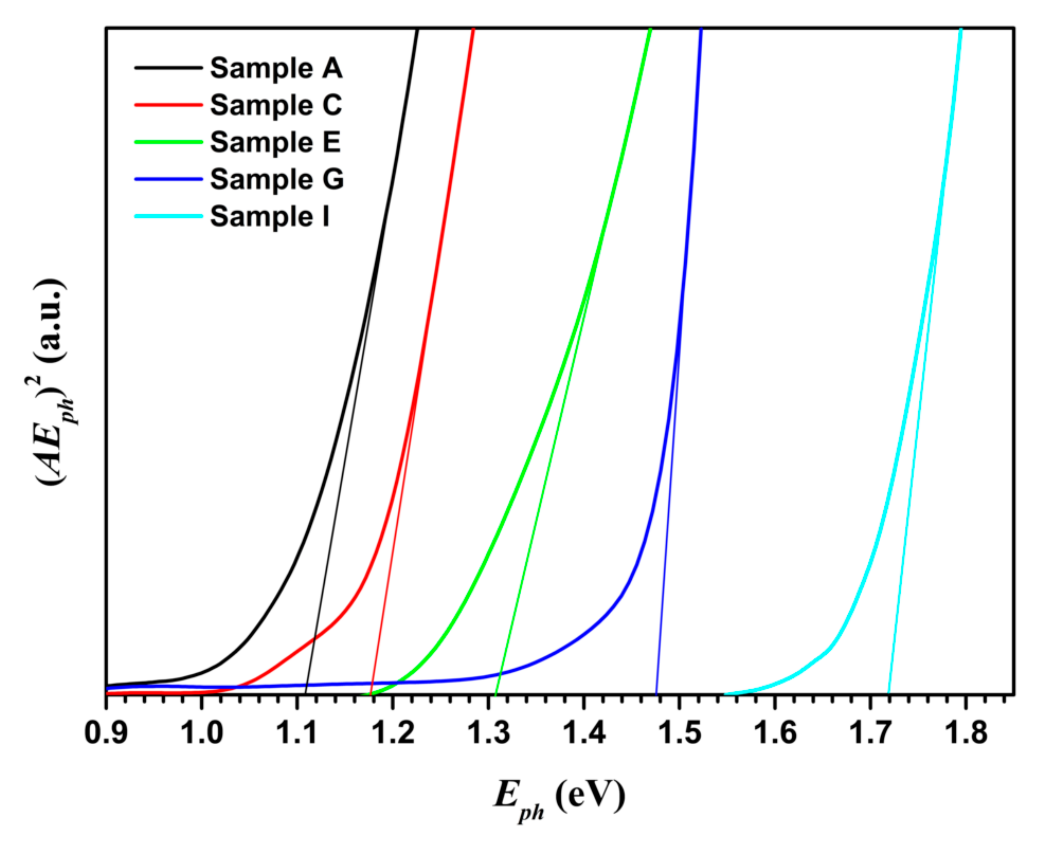
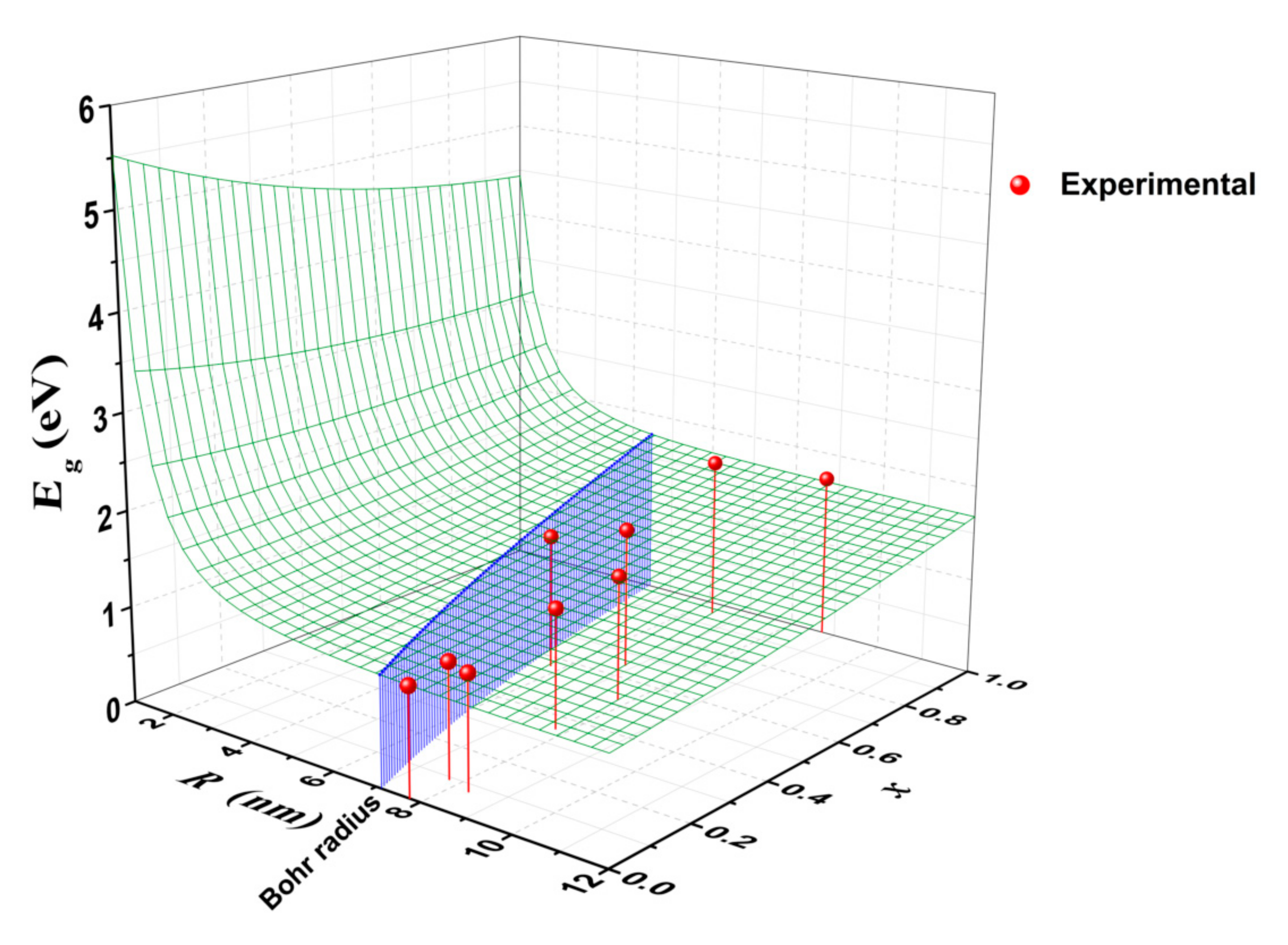
3.3. Determination of Band Gap Energy
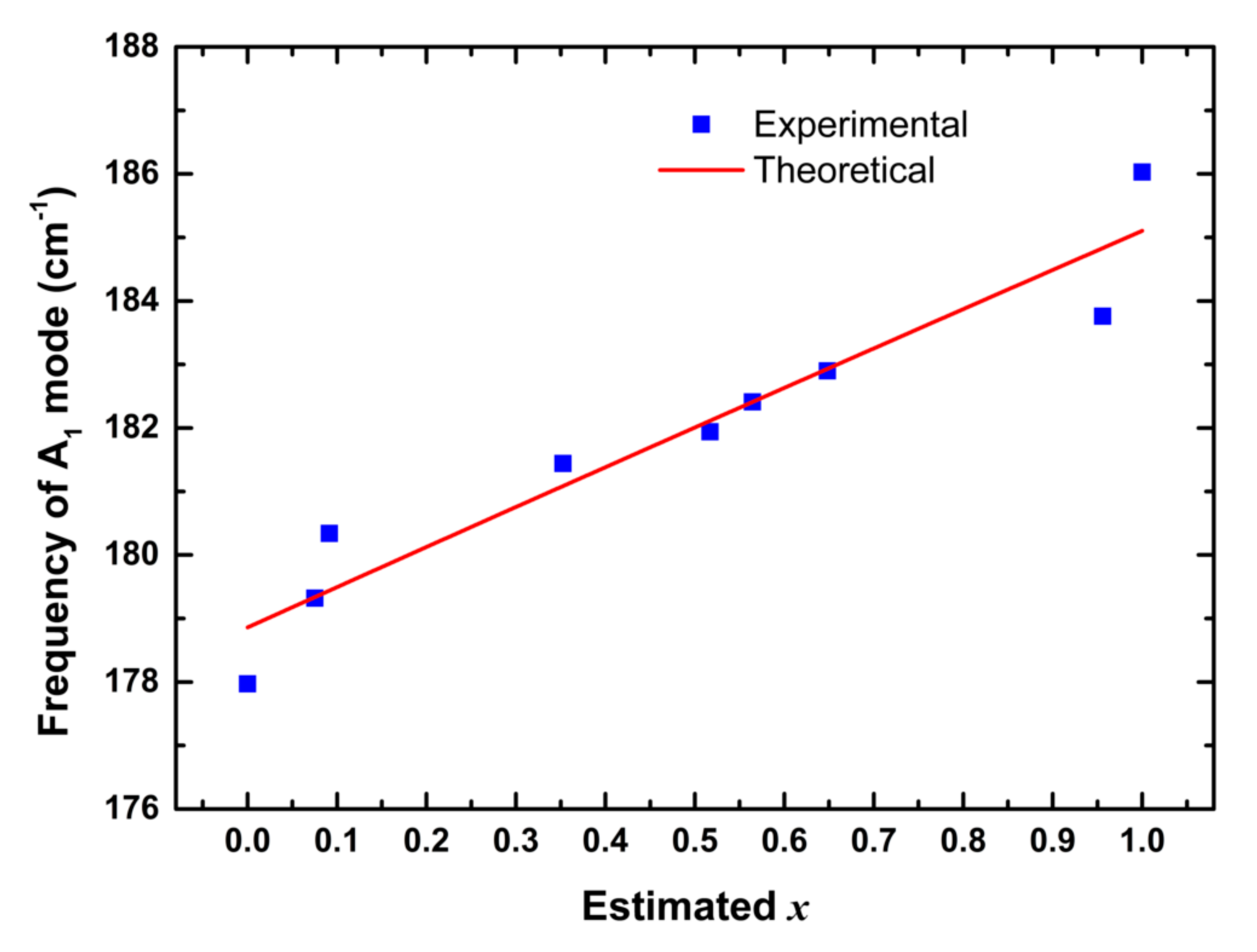
The absorption spectra of the CuIn1−xGaxSe2 nanocrystals were measured at room temperature to investigate their absorption property and determine their optical band gap energy. For a direct-band gap semiconductor, the optical absorption near the band edge has the following behavior [34,35]:
α ( E p h ) = 0 for   E p h < E g , B ( E p h E g ) 1 / 2 E p h for   E p h E g ,
where α is the absorption coefficient, Eph is the incident photon energy, B is a proportional constant, and Eg is the band gap energy, respectively. Since the absorbance A of a sample is proportional to the absorption coefficient α, Equation (6) can be used to determine the optical band gap energy by an absorbance spectrum. Using the Tauc plot [36], as shown in Figure 4 for samples A, C, E, G, and I, the value of Eg could be obtained through extrapolating the linear part of the (AEph)2 vs. Eph curve at (AEph)2 = 0. The band gap energy of the synthesized nanocrystals for samples A to I was found to be 1.108, 1.175, 1.177, 1.250, 1.307, 1.409, 1.476, 1.709, and 1.719 eV, respectively. The uncertainty of these values was about 0.01 eV. These values agree with those reported in other papers [4,21].
According to the effective mass approximation, there is a simple approximation formula which can be used to estimate the band gap energy of a nanocrystal of radius R [37,38]:
E g = E b u l k + ћ 2 π 2 2 μ R 2 1.786 e 2 4 π ε 0 ε r R 0.248 E R y * ,
where Ebulk is the band gap energy of bulk material, μ ≡ 1/(me−1 + mh1) is the reduced mass of an electron-hole pair (me and mh are the effective masses of the electron and the hole, respectively), εr is the dielectric constant, and E*Ry is the effective Rydberg energy:
E R y * = μ 2 ћ 2 e 2 4 π ε 0 ε r 2 .
The first term in Equation (7) represents the quantum confinement energy of an electron-hole pair, the second represents the Coulomb energy, and the third corresponds to the correlation between electron and hole.
The values found in the literature for the parameters in Equation (7) were E b u l k , CuInSe 2 = 1.07 eV [39], m e , CuInSe 2 = 0.09m0 (where m0 is the electron rest mass), m h , CuInSe 2 = 0.73m0 [40], ε r , CuInSe 2 = 10.8 [41] for CuInSe2 and E b u l k , CuGaSe 2 = 1.68 eV [39], m e , CuGaSe 2 = 0.14m0, m h , CuGaSe 2 = 1.20m0 [40], ε r , CuGaSe 2 = 10.6 [41] for CuGaSe2. For CuIn1−xGaxSe2, m e , CuIn 1 x Ga x Se 2 , m h , CuIn 1 x Ga x Se 2 and ε r , CuIn 1 x Ga x Se 2 were assumed to be linearly dependent on x:
m e , CuIn 1 x Ga x Se 2 = ( 1 x ) m e , CuInSe 2 + x m e , CuGaSe 2 m h , CuIn 1 x Ga x Se 2 = ( 1 x ) m h , CuInSe 2 + x m h , CuGaSe 2 ε r , CuIn 1 x Ga x Se 2 = ( 1 x ) ε r , CuInSe 2 + x ε r , CuGaSe 2
and E b u l k , CuIn 1 x Ga x Se 2 could be calculated via the following equation [42,43]:
E b u l k , CuIn 1 x Ga x Se 2 = ( 1 x ) E b u l k , CuInSe 2 + x E b u l k , CuGaSe 2 0.19 x ( 1 x ) eV .
Using Equations (7) to (10), the theoretical band gap energy of a CuIn1−xGaxSe2 nanocrystal was calculated and displayed in Figure 5 as a function of x and R. For reference, the value of exciton Bohr radius of the crystal:
a B = 4 π ε 0 ε r μ e 2
is also shown in Figure 5 as a function of x. When the crystal radius was much smaller than the Bohr radius, the band gap energy decreased rapidly as R increased, and decreased gradually as x increased. However, when the crystal radius was larger than the Bohr radius, the band gap energy decreased slowly as R increased, and increased gradually as x increased.
The experimental values of band gap energy obtained from the absorption measurements are also shown in Figure 5 for comparison. They match well with the theoretically expected values. Since the radii of the synthesized nanocrystals were larger than their corresponding exciton Bohr radii, which were in the range of 4.47–7.13 nm, it would be expected that the primary factor that governs the band gap energy would be their composition ratio of In to Ga, with their size being a secondary factor. Therefore, the experimental band gap energy increased as x increased.

3.4. Raman Analysis

The Raman spectra of the CuIn1−xGaxSe2 nanocrystals recorded at room temperature are shown in Figure 6. The intense peaks observed at around 180 cm−1 were due to the A1 mode [44], which is the strongest signal generally observed in the Raman spectra of I–III–VI2 chalcopyrite compounds. This mode resulted from the vibrations of the two pairs of Se anions in a unit cell of a chalcopyrite structure, i.e., one in the direction of the a-axis and the other in the direction of the b-axis [45]. The peaks observed at around 233 cm−1 may have been due to the B2/E modes of the chalcopyrite crystals [44,45], which represented the vibrations of anions and cations together. There were additional broad peaks at around 260 cm−1 which could be assigned to the A1 mode of Cu-Se compounds [46]. These indicated the appearance of CuxSe in our samples.
Figure 7 shows the frequency of A1 mode as a function of the estimated x. One can see that the A1 mode frequency shifted from 178 to 186 cm−1 with increasing Ga content. This is consistent with previous reports [43,46,47,48]. The A1 mode represented the vibration of the Se anion in the xy plane with the cations at rest. Accordingly, its frequency could be expressed by:
ω A 1 = k Cu - Se + ( 1 x ) k In - Se + x k Ga - Se M Se
where MSe is the mass of Se anion, and kCu-Se, kIn-Se, and kGa-Se are the force constants of the bonds between the Se anions and the Cu, In, and Ga cations, respectively.
Assuming that the force constants were simply proportional to the inverse of the distances between the cations and anions, Equation (12) could be rewritten as:
ω A 1 = C Cu - Se 1 d Cu - Se + C In - Se 1 x d In - Se + C Ga - Se x d Ga - Se
where CCu-Se, CIn-Se, and CGa-Se are constants, and dCu-Se, dIn-Se, and dGa-Se are the interionic distances between the Se anions and the Cu, In, and Ga cations, respectively. Using the ionic radii of Cu (0.96 Å), In (0.81 Å), Ga (0.62 Å), Se (1.98 Å) [27], and the correction ΔN = −0.11 Å for coordination number N = 4 [49], we have dCu-Se = 2.83 Å, dIn-Se = 2.68 Å, dGa-Se = 2.49 Å.
The theoretical plot of the frequency of A1 mode versus x, obtained from Equation (13), shows the same trend as the experimental data. Ga ions are smaller than In ions, which resulted in dGa-Se < dIn-Se and kGa-Se > kIn-Se. Accordingly, the frequency of A1 mode increased with increasing Ga content.

4. Conclusions

In conclusion, CuIn1−xGaxSe2 nanocrystals with varying x value from 0 to 1 were synthesized by a simple solution-based method. According to XRD and TEM results, their particle size was in the range of 11.5–17.4 nm. The nanocrystals had a chalcopyrite structure with decreased lattice constants as the Ga content increased. Using Vegard’s law, the x value of the nanocrystals was determined. From the absorption spectra, the band gap energy of these nanocrystals was determined, which was in the range of 1.11–1.72 eV as the Ga content increased. The variation of band gap energy was primarily governed by the Ga content rather than the crystal size, because the particle radii of these nanocrystals were larger than their corresponding exciton Bohr radii. Raman spectra indicated that the A1 optical vibrational mode of the crystals gradually shifted to a higher wavenumber as the Ga content increased. Assuming that the force constants of bonds were simply proportional to the inverse of distances between the cations and anions, a simple theoretical equation for the A1 mode frequency was proposed. The plot of this equation showed the same trend as the Raman data. Ga ions are smaller than In ions. Accordingly, the frequency of A1 mode increased with increasing Ga content.

Author Contributions

Conceptualization, Y.-T.S.; methodology, Y.-T.S.; validation, Y.-T.S., and Y.-C.T.; formal analysis, Y.-T.S.; investigation, Y.-C.T.; resources, Y.-T.S. and D.-Y.L.; data curation, Y.-T.S., and Y.-C.T.; writing—original draft preparation, Y.-T.S.; writing—review and editing, Y.-T.S. and D.-Y.L.; visualization, Y.-T.S.; supervision, Y.-T.S.; project administration, Y.-T.S.; funding acquisition, Y.-T.S. and D.-Y.L. All authors have read and agreed to the published version of the manuscript.

Funding

This research was funded by the Ministry of Science and Technology (MOST) of the Republic of China, grant numbers MOST-107-2515-S-018-003 and MOST-109-2221-E-018-008, and National Changhua University of Education (NCUE). The article processing charge (APC) was funded by MOST-109-2221-E-018-008.

Conflicts of Interest

The authors declare no conflict of interest.

References

  1. Zhong, H.; Bai, Z.; Zou, B. Tuning the Luminescence Properties of Colloidal I−III−VI Semiconductor Nanocrystals for Optoelectronics and Biotechnology Applications. J. Phys. Chem. Lett. 2012, 3, 3167–3175. [Google Scholar] [CrossRef] [PubMed]
  2. Guillen, C.; Herrero, J. Optical properties of electrochemically deposited CuInSe2 thin films. Sol. Energy Mater. 1991, 23, 31–45. [Google Scholar] [CrossRef]
  3. Rockett, A.; Liao, D.; Heath, J.T.; Cohen, J.D.; Strzhemechny, Y.M.; Brillson, L.J.; Ramanathan, K.; Shafarman, W.N. Near-surface defect distributions in Cu(In,Ga)Se2. Thin Solid Films 2003, 431–432, 301–306. [Google Scholar] [CrossRef]
  4. Marai, A.B.; Belgacem, J.B.; Ayadi, Z.B.; Djessas, K.; Alaya, S. Structural and optical properties of CuIn1−xGaxSe2 nanoparticles synthesized by solvothermal route. J. Alloys Compd. 2016, 658, 961–966. [Google Scholar] [CrossRef]
  5. Latha, M.; Devi, R.A.; Velumani, S. Hot injection synthesis of Cu(In, Ga)Se2 nanocrystals with tunable bandgap. Opt. Mater. 2018, 79, 450–456. [Google Scholar] [CrossRef]
  6. Miyazaki, H.; Mikami, R.; Yamada, A.; Konagai, M. Cu(InGa)Se2 thin film absorber with high Ga contents and its application to the solar cells. J. Phys. Chem. Solid. 2003, 64, 2055–2058. [Google Scholar] [CrossRef]
  7. Sharbati, S.; Gharibshahian, I.; Orouji, A.A. Proposed suitable electron reflector layer materials for thin-film CuIn1−xGaxSe2 solar cells. Opt. Mater. 2018, 75, 216–223. [Google Scholar] [CrossRef]
  8. Jackson, P.; Wuerz, R.; Hariskos, D.; Lotter, E.; Witte, W.; Powalla, M. Effects of heavy alkali elements in Cu(In,Ga)Se2 solar cells with efficiencies up to 22.6%. Phys. Status Solidi Rapid Res. Lett. 2016, 10, 583–586. [Google Scholar] [CrossRef] [Green Version]
  9. Yarema, O.; Yarema, M.; Wood, V. Tuning the composition of multicomponent semiconductor nanocrystals: The case of I–III–VI materials. Chem. Mater. 2018, 30, 1446–1461. [Google Scholar] [CrossRef] [Green Version]
  10. Dilena, E.; Xie, Y.; Brescia, R.; Prato, M.; Maserati, L.; Krahne, R.; Paolella, A.; Bertoni, G.; Povia, M.; Moreels, I.; et al. CuInxGa1xS2 nanocrystals with tunable composition and band gap synthesized via a phosphine-free and scalable procedure. Chem. Mater. 2013, 25, 3180–3187. [Google Scholar] [CrossRef]
  11. Huynh, W.U.; Dittmer, J.J.; Alivisatos, A.P. Hybrid Nanorod-Polymer Solar Cells. Science 2002, 295, 2425–2427. [Google Scholar] [CrossRef] [PubMed] [Green Version]
  12. Gur, I.; Fromer, N.A.; Geier, M.L.; Alivisatos, A.P. Air-stable all-inorganic nanocrystal solar cells processed from solution. Science 2005, 310, 462–465. [Google Scholar] [CrossRef] [PubMed] [Green Version]
  13. Kay, A.; Gratzel, M. Low cost photovoltaic modules based on dye sensitized nanocrystalline titanium dioxide and carbon powder. Sol. Energy Mater. Sol. Cells 1996, 44, 99–117. [Google Scholar] [CrossRef]
  14. Guo, Q.; Ford, G.M.; Yang, W.-C.; Walker, B.C.; Stach, E.A.; Hillhouse, H.W.; Agrawal, R. Fabrication of 7.2% efficient CZTSSe solar cells using CZTS nanocrystals. J. Am. Chem. Soc. 2010, 132, 17384–17386. [Google Scholar] [CrossRef] [PubMed]
  15. Guo, Q.; Ford, G.M.; Hillhouse, H.W.; Agrawal, R. Sulfide nanocrystal inks for dense Cu(In1-xGax)(S1-ySey)2 absorber films and their photovoltaic performance. Nano Lett. 2009, 9, 3060–3065. [Google Scholar] [CrossRef] [PubMed]
  16. Graetzel, M.; Janssen, R.A.J.; Mitzi, D.B.; Sargent, E.H. Materials interface engineering for solution-processed photovoltaics. Nature 2012, 488, 304–312. [Google Scholar] [CrossRef]
  17. Coughlan, C.; Ibaánñez, M.; Dobrozhan, O.; Singh, A.; Cabot, A.; Ryan, K.M. Compound copper chalcogenide nanocrystals. Chem. Rev. 2017, 117, 5865–6109. [Google Scholar] [CrossRef]
  18. Ahmadi, M.; Pramana, S.S.; Xi, L.; Boothroyd, C.; Lam, Y.M.; Mhaisalkar, S. Evolution pathway of CIGSe nanocrystals for solar cell applications. J. Phys. Chem. C 2012, 116, 8202–8209. [Google Scholar] [CrossRef]
  19. Panthani, M.G.; Akhavan, V.; Goodfellow, M.B.; Schmidtke, J.P.; Dunn, L.; Dodabalapur, A.; Barbara, P.F.; Korgel, B.A. Synthesis of CuInS2, CuInSe2, and Cu(InxGa1-x)Se2 (CIGS) Nanocrystal “Inks” for Printable Photovoltaics. J. Am. Chem. Soc. 2008, 130, 16770–16777. [Google Scholar] [CrossRef]
  20. Lauth, J.; Marbach, J.; Meyer, A.; Dogan, S.; Klinke, C.; Kornowski, A.; Weller, H. Virtually bare nanocrystal surfaces: Significantly enhanced electrical transport in CuInSe2 and CuIn1−xGaxSe2 thin films upon ligand exchange with thermally degradable 1-ethyl-5-thiotetrazole. Adv. Funct. Mater. 2014, 24, 1081–1088. [Google Scholar] [CrossRef] [Green Version]
  21. Latha, M.; Devi, R.A.; Velumani, S.; Oza, G.; Reyes-Figueroa, P.; Rohini, M.; Becerril-Juarez, I.G.; Yi, J. Synthesis of CuIn1−xGaxSe2 nanoparticles by thermal decomposition method with tunable Ga content. J. Nanosci. Nanotechnol. 2015, 15, 8388–8394. [Google Scholar] [CrossRef] [PubMed]
  22. Wu, J.D.; Wang, L.T.; Gau, C. Synthesis of CuInGaSe2 nanoparticles by modified polyol route. Sol. Energy Mater. Sol. Cells 2012, 98, 404–408. [Google Scholar]
  23. Rohini, M.; Reyes, P.; Velumani, S.; Latha, M.; Oza, G.; Becerril-Juarez, I.; Asomoza, R. Parametric optimization of mechanochemical process for synthesis of Cu(In,Ga)0.5Se2 nanoparticles. Mater. Sci. Semicond. Process. 2015, 37, 151–158. [Google Scholar] [CrossRef]
  24. Cui, X.; Yun, D.; Zhong, C.; Chen, W.; Cheng, Q.; Feng, J.; Zhang, F. A facile route for synthesis of CuInxGa1−xSe2 nanocrystals with tunable composition for photovoltaic application. J. Sol-Gel Technol. 2015, 76, 469–475. [Google Scholar] [CrossRef]
  25. Houck, D.W.; Nandu, S.V.; Siegler, T.D.; Korgel, B.A. CuGaSe2 and CuInxGa1−xSe2 nanocrystals with sphalerite or wurtzite phase for optoelectronic applications. ACS Appl. Nano Mater. 2019, 2, 4673–4680. [Google Scholar] [CrossRef]
  26. Wang, Y.-H.A.; Zhang, X.; Bao, N.; Lin, B.; Gupta, A. Synthesis of shape-controlled monodisperse wurtzite CuInxGa1−xS2 semiconductor nanocrystals with tunable band gap. J. Am. Chem. Soc. 2011, 133, 11072–11075. [Google Scholar] [CrossRef] [PubMed]
  27. Rohrer, G.S. Structure and Bonding in Crystalline Materials; Cambridge University Press: Cambridge, UK, 2001; p. 478. [Google Scholar]
  28. Balboul, M.R.; Schock, H.W.; Fayak, S.A.; El-Aal, A.A.; Werner, J.H. Correlation of structure parameters of absorber layer with efficiency of Cu(In, Ga)Se2 solar cell. Appl. Phys. A 2008, 92, 557–563. [Google Scholar] [CrossRef]
  29. Benabdeslem, M.; Sehli, H.; Rahal, S.; Benslim, N.; Bechiri, L.; Djekoun, A.; Touam, T.; Boujnah, M.; El Kenz, A.; Benyoussef, A.; et al. Ab initio calculations and experimental properties of CuAlx Ga1−x Te2 for photovoltaic solar cells. J. Electron. Mater. 2016, 45, 1035–1040. [Google Scholar] [CrossRef]
  30. El-Fadl, A.A.; Hassan, A.M.; Kassem, M.A. Structural and spectroscopic studies of nanocrystalline Ni1−xMgxFe2O4 ferrites synthesized by a microwave-assisted combustion route. Phys. Scr. 2020, 95, 055813. [Google Scholar] [CrossRef]
  31. Xu, Y.; Fu, Q.; Lei, S.; Lai, L.; Xiong, J.; Bian, Q.; Xiao, Y.; Cheng, B. Preparation of quinary CuNixZn2−xInS4 nanocrystals with wurtzite structure and tunable band gap. J. Alloys Compd. 2020, 820, 153436. [Google Scholar] [CrossRef]
  32. Cullity, B.D.; Stock, S.R. Elements of X-Ray Diffraction, 3rd ed.; Prentice-Hall: Upper Saddle River, NJ, USA, 2001; p. 264. [Google Scholar]
  33. Ghali, M.; Elnimr, M.; Ali, G.F.; Yousif, B. Colloidal CuInSe2 nanocrystals and thin films for low-cost photovoltaics. Opt. Mater. 2016, 55, 145–152. [Google Scholar] [CrossRef]
  34. Bhattacharya, P. Semiconductor Optoelectronic Devices, 2nd ed.; Prentice-Hall: Upper Saddle River, NJ, USA, 1997; p. 124. [Google Scholar]
  35. Peyghambarian, N.; Koch, S.W.; Mysyrowicz, A. Introduction to Semiconductor Optics; Prentice-Hall: Englewood Cliffs, NJ, USA, 1993; p. 127. [Google Scholar]
  36. Tauc, J.; Grigorvici, R.; Vancu, A. Optical properties and electronic structure of amorphous germanium. Phys. Status Solidi 1966, 15, 627–637. [Google Scholar] [CrossRef]
  37. Brus, L.E. Electron–electron and electron-hole interactions in small semiconductor crystallites: The size dependence of the lowest excited electronic state. J. Chem. Phys. 1984, 80, 4403. [Google Scholar] [CrossRef] [Green Version]
  38. Kayanuma, Y. Quantum-size effects of interacting electrons and holes in semiconductor microcrystals with spherical shape. Phys. Rev. B 1988, 38, 9797–9805. [Google Scholar] [CrossRef]
  39. Omata, T.; Nose, K.; Otsuka-Yao-Matsuo, S. Size dependent optical band gap of ternary I-III-VI2 semiconductor nanocrystals. J. Appl. Phys. 2009, 105, 073106. [Google Scholar] [CrossRef]
  40. Rincon, C.; Gonzalez, J. Acoustic deformation potentials in AIBIIIC2VI chalcopyrite semiconductors. Phys. Rev. B 1989, 40, 8552–8554. [Google Scholar] [CrossRef]
  41. Persson, C. Anisotropic hole-mass tensor of CuIn1−xGax(S,Se)2: Presence of free carriers narrows the energy gap. Appl. Phys. Lett. 2008, 93, 072106. [Google Scholar] [CrossRef]
  42. Wei, S.-H.; Zunger, A. Band offsets and optical bowings of chalcopyrites and Zn-based II-VI alloys. J. Appl. Phys. 1995, 78, 3846–3856. [Google Scholar] [CrossRef] [Green Version]
  43. Jeong, A.R.; Jo, W.; Song, M.; Yoon, S. Crystalline ordered states of CuIn1−xGaxSe2 (x = 0, 0.3, and 1.0) thin-films on different substrates investigated by Raman scattering spectroscopy. Mater. Chem. Phys. 2012, 134, 1030–1035. [Google Scholar] [CrossRef]
  44. Rincon, C.; Ramirez, F.J. Lattice vibrations of CuInSe2 and CuGaSe2 by Raman microspectrometry. J. Appl. Phys. 1992, 72, 4321–4324. [Google Scholar] [CrossRef]
  45. Matsushita, H.; Endo, S.; Irie, T. Raman-scattering properties of I-III-VI2 group chalcopyrite semiconductors. Jpn. J. Appl. Phys. 1992, 31, 18–22. [Google Scholar] [CrossRef]
  46. Witt, W.; Kniese, R.; Powalla, M. Raman investigations of Cu(In,Ga)Se2 thin films with various copper contents. Thin Solid Films 2008, 517, 867–869. [Google Scholar] [CrossRef]
  47. Roy, S.; Guha, P.; Kundu, S.N.; Hanzawa, H.; Chaudhuri, S.; Pal, A.K. Characterization of Cu(In,Ga)Se2 films by Raman scattering. Mater. Chem. Phys. 2002, 73, 24–30. [Google Scholar] [CrossRef]
  48. Olejnicek, J.; Kamler, C.A.; Mirasano, A.; Martinez-Skinner, A.L.; Ingersoll, M.A.; Exstrom, C.L.; Darveau, S.A.; Huguenin-Love, J.L.; Diaz, M.; Ianno, N.J.; et al. A non-vacuum process for preparing nanocrystalline CuIn1−xGaxSe2 materials involving an open-air solvothermal reaction. Sol. Energy Mater. Sol. Cells 2010, 94, 8–11. [Google Scholar] [CrossRef] [Green Version]
  49. Kittel, C. Introduction to Solid State Physics, 7th ed.; John Wiley & Sons: Hoboken, NJ, USA, 1996; p. 79. [Google Scholar]
Figure 1. X-ray diffraction patterns of CuIn1−xGaxSe2 nanocrystals.
Nanomaterials 10 02066 g001
Figure 2. Lattice constants of CuIn1−xGaxSe2 nanocrystals as functions of estimated x.
Nanomaterials 10 02066 g002
Figure 3. TEM images of CuIn1−xGaxSe2 nanocrystals: (a) Sample A, (b) Sample D, (c) Sample F, (d) Sample A, (e) Sample B, (f) Sample C, (g) Sample D, (h) Sample E, (i) Sample F, (j) Sample G, (k) Sample H, (l) Sample I.
Nanomaterials 10 02066 g003
Figure 4. Tauc plot of (AEph)2 versus Eph of CuIn1−xGaxSe2 nanocrystals.
Nanomaterials 10 02066 g004
Figure 5. Band gap energy of CuIn1−xGaxSe2 nanocrystals as a function of x and R.
Nanomaterials 10 02066 g005
Figure 6. Raman spectra of CuIn1−xGaxSe2 nanocrystals.
Nanomaterials 10 02066 g006
Figure 7. Frequency of A1 mode of CuIn1−xGaxSe2 nanocrystals as a function of estimated x.
Nanomaterials 10 02066 g007
Table 1. Structural and optical parameters of CuIn1−xGaxSe2 nanocrystals.
SampleNominal xd112 (Å)a (Å)c (Å)Estimated xCrystallite Size (nm)Gap Energy (eV)Raman Shift (cm−1)
A03.3625.79411.764015.5281.108 ± 0.01177.97 ± 1.52
B0.1253.3535.78211.7210.07516.7111.175 ± 0.01179.32 ± 0.53
C0.253.3515.77911.7120.09115.5331.177 ± 0.01180.34 ± 1.29
D0.3753.3235.74511.5550.35315.5301.250 ± 0.01181.44 ± 1.10
E0.53.3115.74311.4380.51715.5371.307 ± 0.01181.94 ± 0.48
F0.6253.3025.72211.4240.56411.5011.409 ± 0.01182.41 ± 0.53
G0.753.2885.69311.3910.64813.6591.476 ± 0.01182.90 ± 0.48
H0.8753.2475.62811.2320.95612.8181.709 ± 0.01183.76 ± 0.68
I13.2375.60411.223117.,4421.719 ± 0.01186.03 ± 0.86
Publisher’s Note: MDPI stays neutral with regard to jurisdictional claims in published maps and institutional affiliations.

