Narrowband Light Reflection Resonances from Waveguide Modes for High-Quality Sensors

Abstract
:1. Introduction
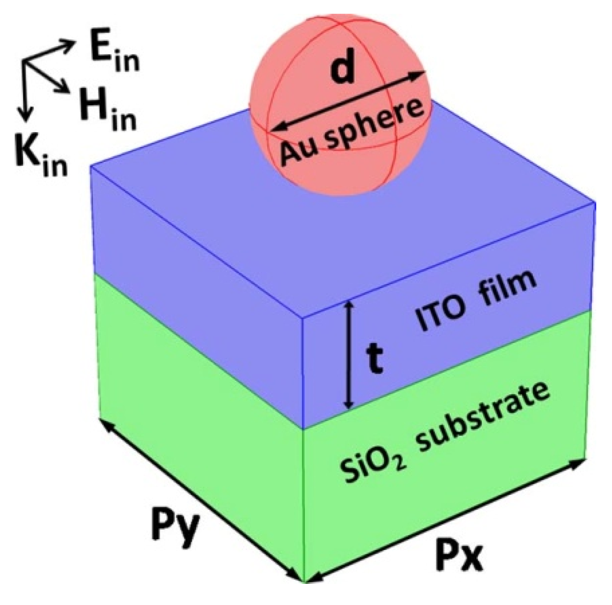
2. Methods
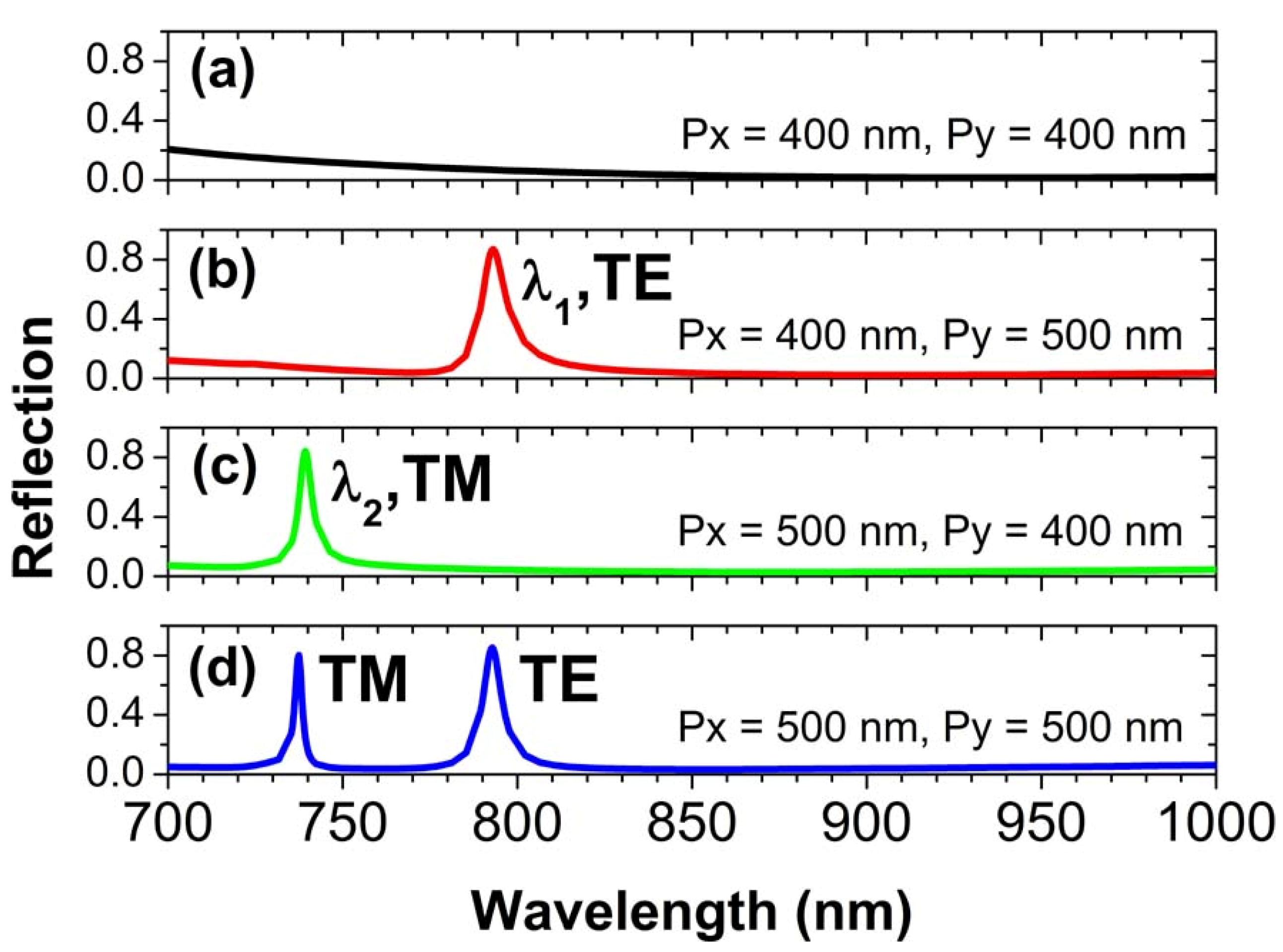
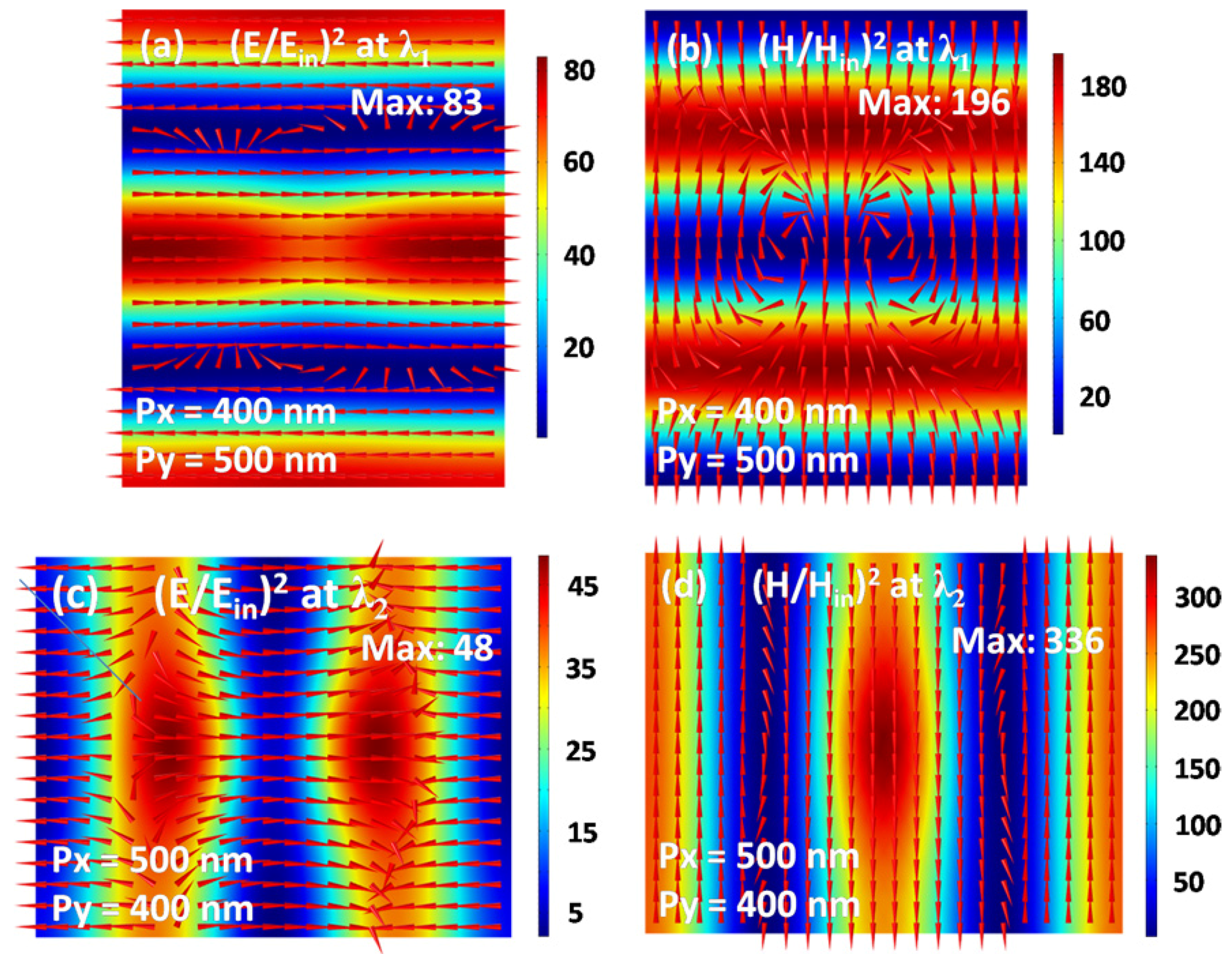
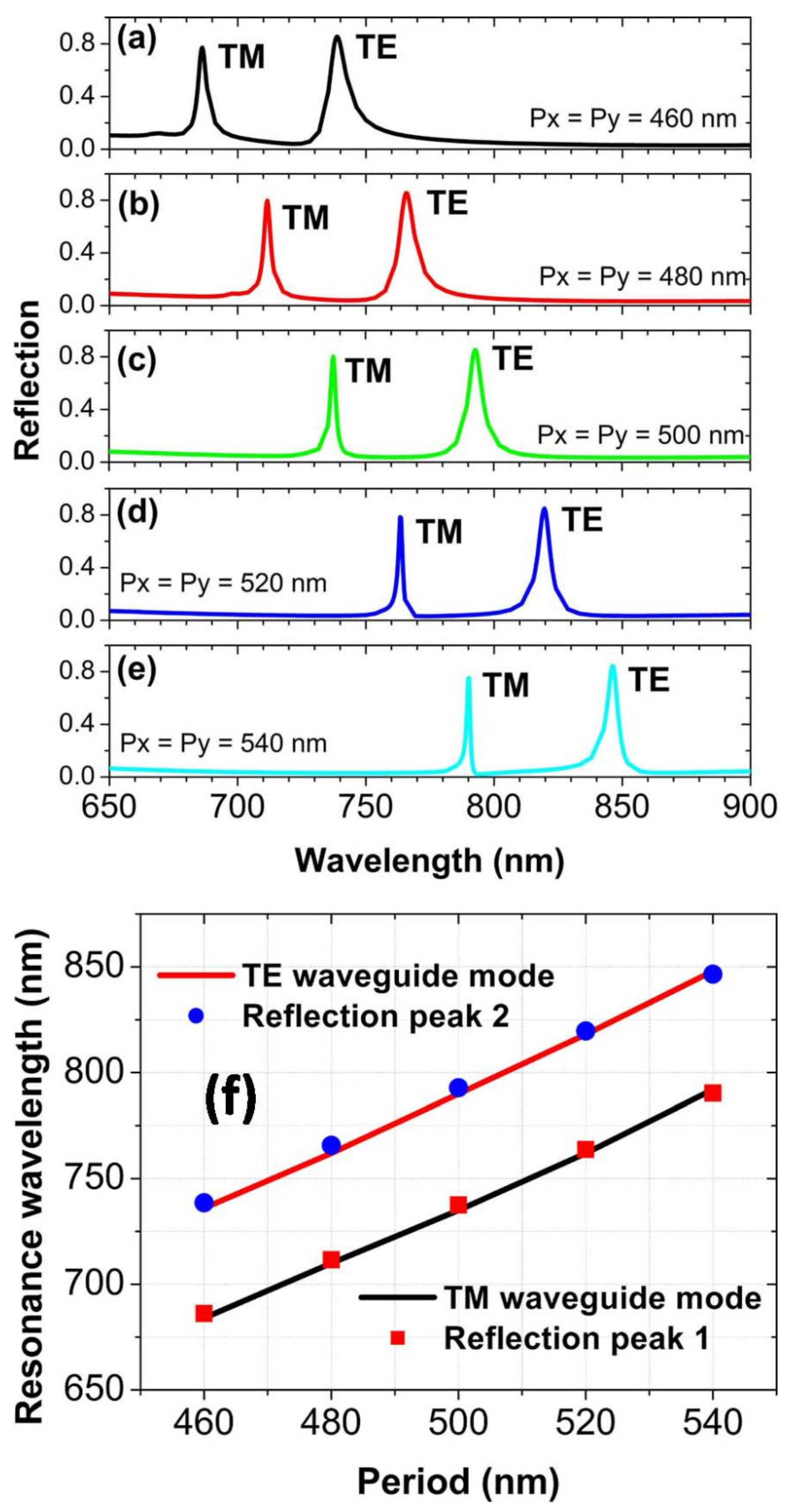
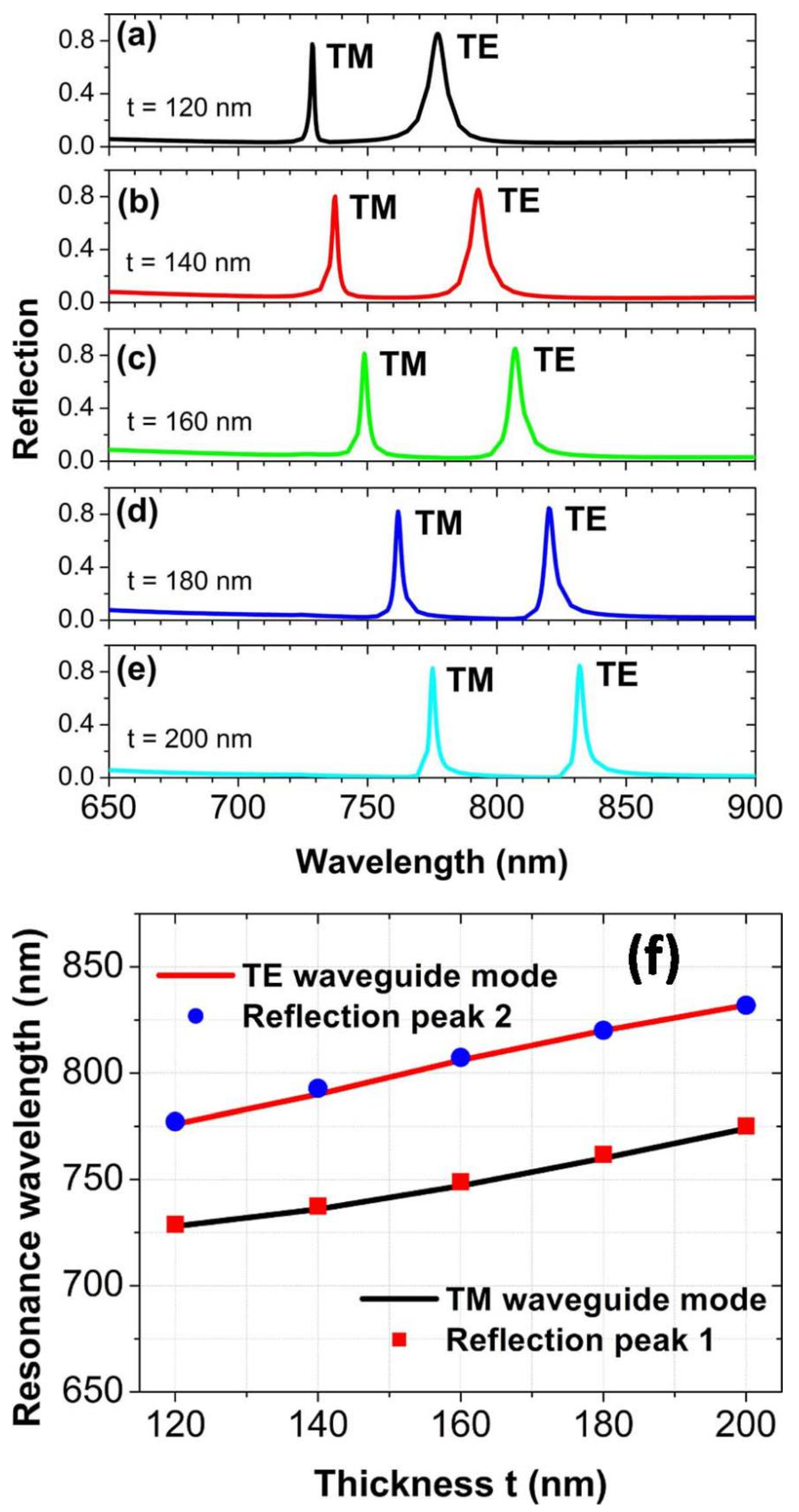
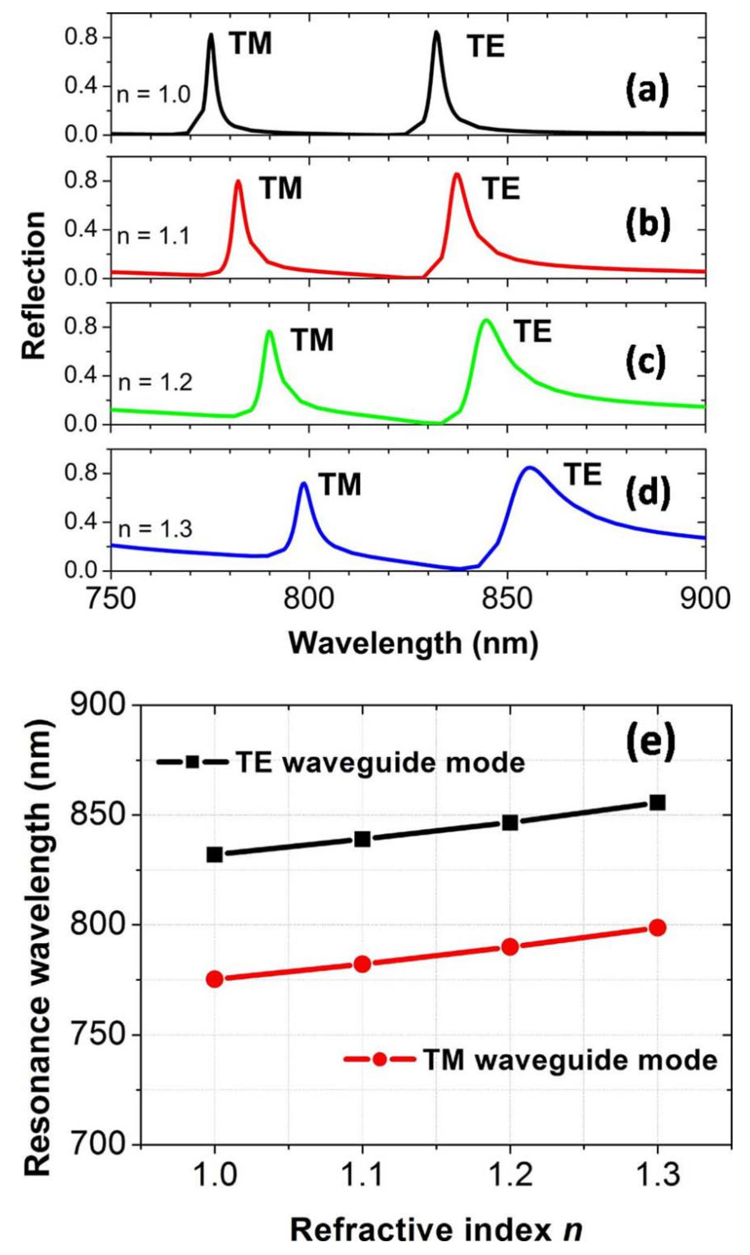
3. Results and Discussion
θ1 > sin−1(n0/n1),
β = kn1sinθ1 = G,
tanΦ12 = √(n12sin2θ1 − n02)/(n1cosθ1)
tanΦ12 = √(n12sin2θ1 – n02)/(n02n1cosθ1)
4. Conclusions
Author Contributions
Funding
Conflicts of Interest
References
- Homola, J. Surface plasmon resonance sensors for detection of chemical and biological species. Chem. Rev. 2008, 108, 462–493. [Google Scholar] [CrossRef] [PubMed]
- Mayer, K.M.; Hafner, J.H. Localized surface plasmon resonance sensors. Chem. Rev. 2011, 111, 3828–3857. [Google Scholar] [CrossRef] [PubMed]
- Xue, T.Y.; Liang, W.Y.; Li, Y.W.; Sun, Y.H.; Xiang, Y.J.; Zhang, Y.P.; Dai, Z.G.; Duo, Y.H.; Wu, L.M.; Qi, K.; et al. Ultrasensitive detection of miRNA with an antimonene-based surface plasmon resonance sensor. Nat. Commun 2019, 10, 28. [Google Scholar] [CrossRef]
- Li, M.; Cushing, S.K.; Wu, N.Q. Plasmon-enhanced optical sensors: A review. Analyst 2015, 140, 386–406. [Google Scholar] [CrossRef] [PubMed] [Green Version]
- Roh, S.; Chung, T.; Lee, B. Overview of the characteristics of micro- and nano-structured surface plasmon resonance sensors. Sensors 2011, 11, 1565–1588. [Google Scholar] [CrossRef] [PubMed] [Green Version]
- Wong, C.L.; Olivo, M. Surface plasmon resonance imaging sensors: A review. Plasmonics 2014, 9, 809–824. [Google Scholar] [CrossRef]
- White, I.M.; Fan, X.D. On the performance quantification of resonant refractive index sensors. Opt. Express 2008, 16, 1020–1028. [Google Scholar] [CrossRef] [Green Version]
- Piliarik, M.; Homola, J. Surface plasmon resonance (SPR) sensors: Approaching their limits? Opt. Express 2009, 17, 16505–16517. [Google Scholar] [CrossRef]
- Shalabney, A.; Abdulhalim, I. Sensitivity-enhancement methods for surface plasmon sensors. Laser Photonics Rev. 2011, 5, 571–606. [Google Scholar] [CrossRef]
- Chen, X.; Xia, L.; Li, C. Surface plasmon resonance sensor based on a novel d-shaped photonic crystal fiber for low refractive index detection. IEEE Photonics J. 2018, 10, 6800709. [Google Scholar] [CrossRef]
- Huang, Y.; Min, C.J.; Dastmalchi, P.; Veronis, G. Slow-light enhanced subwavelength plasmonic waveguide refractive index sensors. Opt. Express 2015, 23, 14922–14936. [Google Scholar] [CrossRef] [PubMed]
- Lahav, A.; Auslender, M.; Abdulhalim, I. Sensitivity enhancement of guided-wave surface-plasmon resonance sensors. Opt. Lett. 2008, 33, 2539–2541. [Google Scholar] [CrossRef] [PubMed]
- Liu, Z.Q.; Yu, M.D.; Huang, S.; Liu, X.S.; Wang, Y.; Liu, M.L.; Pan, P.P.; Liu, G.Q. Enhancing refractive index sensing capability with hybrid plasmonic-photonic absorbers. J. Mater. Chem. C 2015, 3, 4222–4226. [Google Scholar] [CrossRef]
- Zhou, J.; Liu, X.S.; Fu, G.L.; Liu, G.Q.; Tang, P.; Yuan, W.; Zhan, X.F.; Liu, Z.Q. High-performance plasmonic oblique sensors for the detection of ions. Nanotechnology 2020, 31, 285501. [Google Scholar] [CrossRef] [PubMed]
- Liu, Z.Q.; Liu, G.Q.; Liu, X.S.; Fu, G.L. Plasmonic sensors with an ultra-high figure of merit. Nanotechnology 2020, 31, 115208. [Google Scholar] [CrossRef] [PubMed]
- Liu, G.Q.; Liu, Y.; Tang, L.; Liu, X.S.; Fu, G.L.; Liu, Z.Q. Semiconductor-enhanced Raman scattering sensors via quasi-three-dimensional Au/Si/Au structures. Nanophotonics 2019, 8, 1095–1107. [Google Scholar] [CrossRef]
- Hao, F.; Nordlander, P.; Sonnefraud, Y.; Dorpe, P.V.; Maier, S.A. Tunability of subradiant dipolar and Fano-type plasmon resonances in metallic ring/disk cavities: Implications for nanoscale optical sensing. Acs Nano 2009, 3, 643–652. [Google Scholar] [CrossRef]
- King, N.S.; Liu, L.F.; Yang, X.; Cerjan, B.; Everitt, H.O.; Nordlander, P.; Halas, N.J. Fano resonant aluminum nanoclusters for plasmonic colorimetric sensing. Acs Nano 2015, 9, 10628–10636. [Google Scholar] [CrossRef]
- Singh, R.; Cao, W.; Al-Naib, I.; Cong, L.Q.; Withayachumnankul, W.; Zhang, W.L. Ultrasensitive terahertz sensing with high-Q Fano resonances in metasurfaces. Appl. Phys. Lett. 2011, 105, 171101. [Google Scholar] [CrossRef] [Green Version]
- Hao, F.; Sonnefraud, Y.; Dorpe, P.V.; Maier, S.A.; Halas, N.J.; Nordlander, P. Symmetry breaking in plasmonic nanocavities: Subradiant LSPR sensing and a tunable Fano resonance. Nano Lett. 2008, 8, 3983–3988. [Google Scholar] [CrossRef]
- Zhang, S.P.; Bao, K.; Halas, N.J.; Xu, H.X.; Nordlander, P. Substrate-induced Fano resonances of a plasmonic nanocube: A route to increased-sensitivity localized surface plasmon resonance sensors revealed. Nano Lett. 2011, 11, 1657–1663. [Google Scholar] [CrossRef] [PubMed]
- Zhan, Y.H.; Lei, D.Y.; Li, X.F.; Maier, S.A. Plasmonic Fano resonances in nanohole quadrumers for ultra-sensitive refractive index sensing. Nanoscale 2014, 6, 4705–4715. [Google Scholar] [CrossRef] [PubMed]
- Zhang, Y.P.; Li, T.T.; Zeng, B.B.; Zhang, H.Y.; Lv, H.H.; Huang, X.Y.; Zhang, W.L.; Azad, A.K. A graphene based tunable terahertz sensor with double Fano resonances. Nanoscale 2015, 7, 12682–12688. [Google Scholar] [CrossRef]
- Wang, J.Q.; Fan, C.Z.; He, J.N.; Ding, P.; Liang, E.J.; Xue, Q.Z. Double Fano resonances due to interplay of electric and magnetic plasmon modes in planar plasmonic structure with high sensing sensitivity. Opt. Express 2013, 21, 2236–2244. [Google Scholar] [CrossRef]
- Chen, J.J.; Li, Z.; Zou, Y.J.; Deng, Z.L.; Xiao, J.H.; Gong, Q.H. Coupled-resonator-induced Fano resonances for plasmonic sensing with ultra-high figure of merits. Plasmonics 2013, 8, 1627–1631. [Google Scholar] [CrossRef]
- Chen, Y.; Xu, Y.M.; Cao, J.G. Fano resonance sensing characteristics of MIM waveguide coupled square convex ring resonator with metallic baffle. Results Phys. 2019, 14, 102420. [Google Scholar] [CrossRef]
- Su, W.; Ding, Y.M.; Luo, Y.L.; Liu, Y. A high figure of merit refractive index sensor based on Fano resonance in all-dielectric metasurface. Results Phys. 2020, 16, 102833. [Google Scholar] [CrossRef]
- He, Z.H.; Xue, W.W.; Cui, W.; Li, C.J.; Li, Z.X.; Pu, L.H.; Feng, J.J.; Xiao, X.T.; Wang, X.Y.; Li, G. Tunable Fano resonance and enhanced sensing in a simple Au/TiO2 hybrid metasurface. Nanomaterials 2020, 10, 687. [Google Scholar] [CrossRef] [Green Version]
- Amin, M.; Farhat, M.; Bagci, H. A dynamically reconfigurable Fano metamaterial through graphene tuning for switching and sensing applications. Sci. Rep. 2013, 3, 2105. [Google Scholar] [CrossRef] [Green Version]
- Chen, J.; Yuan, J.; Zhang, Q.; Ge, H.M.; Tang, C.J.; Liu, Y.; Guo, B.N. Dielectric waveguide-enhanced localized surface plasmon resonance refractive index sensing. Opt. Mater. Express 2018, 8, 342–347. [Google Scholar] [CrossRef]
- Ameling, R.; Langguth, L.; Hentschel, M.; Mesch, M.; Braun, P.V.; Giessen, H. Cavity-enhanced localized plasmon resonance sensing. Appl. Phys. Lett. 2010, 97, 253116. [Google Scholar] [CrossRef]
- Liu, N.; Mesch, M.; Weiss, T.; Hentschel, M.; Giessen, H. Infrared perfect absorber and its application as plasmonic sensor. Nano Lett. 2010, 10, 2342–2348. [Google Scholar] [CrossRef] [PubMed]
- Yong, Z.D.; Zhang, S.L.; Gong, C.S.; He, S.L. Narrow band perfect absorber for maximum localized magnetic and electric field enhancement and sensing applications. Sci. Rep. 2016, 6, 24063. [Google Scholar] [CrossRef] [PubMed] [Green Version]
- Chen, J.; Nie, H.; Tang, C.J.; Cui, Y.H.; Yan, B.; Zhang, Z.Y.; Kong, Y.R.; Xu, Z.J.; Cai, P.G. Highly sensitive refractive-index sensor based on strong magnetic resonance in metamaterials. Appl. Phys. Express 2019, 12, 052015. [Google Scholar] [CrossRef]
- Bagheri, S.H.; Strohfeldt, N.; Sterl, F.; Berrier, A.; Tittl, A.; Giessen, H. Large-area low-cost plasmonic perfect absorber chemical sensor fabricated by laser interference lithography. Acs Sens. 2016, 1, 1148–1154. [Google Scholar] [CrossRef]
- Li, G.H.; Chen, X.S.; Li, O.P.; Shao, C.G.; Jiang, Y.; Huang, L.J.; Ni, B.; Hu, W.D.; Lu, W. A novel plasmonic resonance sensor based on an infrared perfect absorber. J. Phys. D Appl. Phys. 2012, 45, 205102. [Google Scholar] [CrossRef]
- Wu, D.; Li, R.F.; Liu, Y.M.; Yu, Z.Y.; Yu, L.; Chen, L.; Liu, C.; Ma, R.; Ye, H. Ultra-narrow band perfect absorber and its application as plasmonic sensor in the visible region. Nanoscale Res. Lett. 2017, 12, 427. [Google Scholar] [CrossRef]
- Liu, X.S.; Fu, G.L.; Zhan, X.F.; Liu, Z.Q. All-metal resonant metamaterials for one-, two-, three-band perfect light absorbers and sensors. Plasmonics 2019, 14, 967–971. [Google Scholar] [CrossRef]
- Cui, W.L.; Peng, W.; Yu, L.; Luo, X.L.; Gao, H.X.; Chu, S.W.; Masson, J.F. Hybrid nanodisk film for ultra-narrowband filtering, near-perfect absorption and wide range. Nanomaterials 2019, 9, 334. [Google Scholar] [CrossRef] [Green Version]
- Liao, Y.L.; Zhao, Y. Ultra-narrowband dielectric metamaterial absorber for sensing based on cavity-coupled phase resonance. Results Phys. 2020, 17, 103072. [Google Scholar] [CrossRef]
- Feng, S.J.; Zhao, Y.; Liao, Y.L. Dual-band dielectric metamaterial absorber and sensing applications. Results Phys. 2020, 18, 103272. [Google Scholar] [CrossRef]
- Liao, Y.L.; Zhao, Y. Ultra-narrowband dielectric metamaterial absorber with ultrasparse nanowire grids for sensing applications. Sci. Rep. 2020, 10, 1480. [Google Scholar] [CrossRef] [PubMed] [Green Version]
- Liu, B.; Tang, C.J.; Chen, J.; Xie, N.Y.; Yuan, J.; Tang, H.; Zhu, X.Q. Metal-substrate-enhanced magnetic dipole resonance in metamaterials for high-performance refractive index sensing. Opt. Mater. Express 2018, 8, 2008–2016. [Google Scholar] [CrossRef]
- Chen, J.; Fan, W.F.; Zhang, T.; Tang, C.J.; Chen, X.Y.; Wu, J.J.; Li, D.Y.; Ying, Y. Engineering the magnetic plasmon resonances of metamaterials for high-quality sensing. Opt. Express 2017, 25, 3675–3681. [Google Scholar] [CrossRef]
- Wu, P.C.; Sun, G.; Chen, W.T.; Yang, K.Y.; Huang, Y.W.; Chen, Y.H.; Huang, H.L.; Hsu, W.L.; Chiang, H.P.; Tsai, D.P. Vertical split-ring resonator based nanoplasmonic sensor. Appl. Phys. Lett. 2014, 105, 033105. [Google Scholar] [CrossRef]
- Wu, P.C.; Liao, C.Y.; Chen, J.W.; Tsai, D.P. Isotropic absorption and sensor of vertical split-ring resonator. Adv. Opt. Mater. 2017, 5, 1600581. [Google Scholar] [CrossRef]
- Johnson, P.B.; Christy, R.W. Optical constants of the noble metals. Phys. Rev. B 1972, 6, 4370–4379. [Google Scholar] [CrossRef]
- Yannopapas, V.; Stefanou, N. Optical excitation of coupled waveguide-particle plasmon modes: A theoretical analysis. Phys. Rev. B 2004, 69, 012408. [Google Scholar] [CrossRef]
- Liu, B.; Tang, C.J.; Chen, J.; Zhu, M.W.; Pei, M.X.; Zhu, X.Q. Electrically tunable Fano resonance from the coupling between interband transition in monolayer graphene and magnetic dipole in metamaterials. Sci. Rep. 2017, 7, 17117. [Google Scholar] [CrossRef] [Green Version]
- Liu, B.; Tang, C.J.; Chen, J.; Yan, Z.D.; Zhu, M.W.; Sui, Y.X.; Tang, H. The coupling effects of surface plasmon polaritons and magnetic dipole resonances in metamaterials. Nanoscale Res. Lett. 2017, 12, 586. [Google Scholar] [CrossRef]
- Liu, B.; Tang, C.J.; Chen, J.; Xie, N.Y.; Zheng, L.; Wang, S. Tri-band absorption enhancement in monolayer graphene in the visible spectrum due to multiple plasmon resonances in metal-insulator-metal nanostructure. Appl. Phys. Express 2018, 11, 072201. [Google Scholar] [CrossRef]
- Tien, P.K. Light waves in thin films and integrated optics. Appl. Opt. 1971, 10, 2395–2413. [Google Scholar] [CrossRef] [PubMed]
- Chen, J.; Nie, H.; Peng, C.; Qi, S.B.; Tang, C.J.; Zhang, Y.; Wang, L.H.; Park, G.S. Enhancing the magnetic plasmon resonance of 3D optical metamaterials via strong coupling for high-sensitivity sensing. J. Lightwave Technol. 2018, 36, 3481–3485. [Google Scholar] [CrossRef]
- Ji, Y.Q.; Tang, C.J.; Xie, N.Y.; Chen, J.; Gu, P.; Peng, C.; Liu, B. High-performance metamaterial sensors based on strong coupling between surface plasmon polaritons and magnetic plasmon resonances. Results Phys. 2019, 14, 102397. [Google Scholar] [CrossRef]
- Chen, J.; Qi, S.B.; Hong, X.H.; Gu, P.; Wei, R.Q.; Tang, C.J.; Huang, Y.L.; Zhao, C.Y. Highly sensitive 3D metamaterial sensor based on diffraction coupling of magnetic plasmon resonances. Results Phys. 2019, 15, 102791. [Google Scholar] [CrossRef]
- Chau, Y.F.C.; Chen, K.H.; Chiang, H.P.; Lim, C.M.; Huang, H.J.; Lai, C.H.; Kumara, N.T.R.N. Fabrication and characterization of a metallic-dielectric nanorod array by nanosphere lithography for plasmonic sensing application. Nanomaterials 2019, 9, 1691. [Google Scholar] [CrossRef] [Green Version]
- Farcau, C.; Marconi, D.; Colnita, A.; Brezestean, I.; Barbu-Tudoran, L. Gold nanopost-shell arrays fabricated by nanoimprint lithography as a flexible plasmonic sensing platform. Nanomaterials 2019, 9, 1519. [Google Scholar] [CrossRef] [Green Version]
© 2020 by the authors. Licensee MDPI, Basel, Switzerland. This article is an open access article distributed under the terms and conditions of the Creative Commons Attribution (CC BY) license (http://creativecommons.org/licenses/by/4.0/).
Share and Cite
Gu, P.; Chen, J.; Yang, C.; Yan, Z.; Tang, C.; Cai, P.; Gao, F.; Yan, B.; Liu, Z.; Huang, Z. Narrowband Light Reflection Resonances from Waveguide Modes for High-Quality Sensors. Nanomaterials 2020, 10, 1966. https://doi.org/10.3390/nano10101966
Gu P, Chen J, Yang C, Yan Z, Tang C, Cai P, Gao F, Yan B, Liu Z, Huang Z. Narrowband Light Reflection Resonances from Waveguide Modes for High-Quality Sensors. Nanomaterials. 2020; 10(10):1966. https://doi.org/10.3390/nano10101966
Chicago/Turabian StyleGu, Ping, Jing Chen, Chun Yang, Zhendong Yan, Chaojun Tang, Pinggen Cai, Fan Gao, Bo Yan, Zhengqi Liu, and Zhong Huang. 2020. "Narrowband Light Reflection Resonances from Waveguide Modes for High-Quality Sensors" Nanomaterials 10, no. 10: 1966. https://doi.org/10.3390/nano10101966
APA StyleGu, P., Chen, J., Yang, C., Yan, Z., Tang, C., Cai, P., Gao, F., Yan, B., Liu, Z., & Huang, Z. (2020). Narrowband Light Reflection Resonances from Waveguide Modes for High-Quality Sensors. Nanomaterials, 10(10), 1966. https://doi.org/10.3390/nano10101966