Towards Highly Efficient TADF Yellow-Red OLEDs Fabricated by Solution Deposition Methods: Critical Influence of the Active Layer Morphology


Abstract

1. Introduction
2. Materials and Methods
2.1. Materials
2.2. Device Fabrication
2.3. Optical and Electrical Measurements
3. Results and Discussion
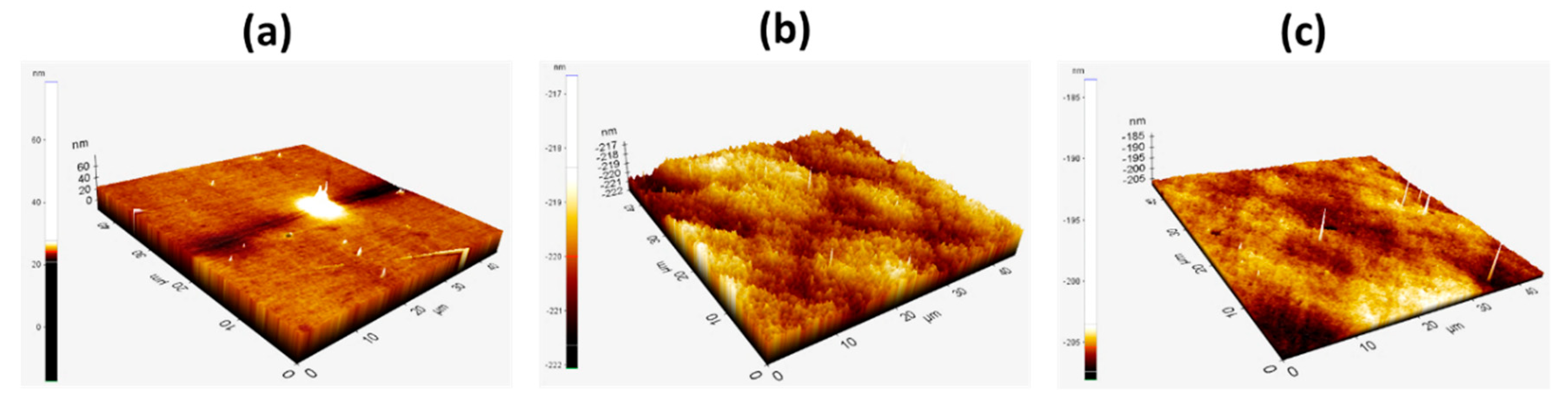
3.1. Photophysical Characterization and Film Morphology
3.2. Device Characterization
3.2.1. Devices with an Emissive Layer Using Chloroform as a Solvent
3.2.2. Devices with an Emissive Layer Using Dichlorobenzene as a Solvent
3.2.3. Devices with an Emissive Layer Using Chlorobenzene as a Solvent
4. Conclusions
Supplementary Materials
Author Contributions
Funding
Acknowledgments
Conflicts of Interest
References
- Yersin, H. Highly Efficient OLEDs with Phosphorescent Materials; John Wiley & Sons: New York, NY, USA, 2008. [Google Scholar]
- So, F. Organic Electronics: Materials, Processing, Devices and Applications; CRC Press: Boca Raton, FL, USA, 2009. [Google Scholar]
- Gaspar, D.J.; Polikarpov, E. OLED Fundamentals: Materials, Devices, and Processing of Organic Light-Emitting Diodes; CRC press: Boca Raton, FL, USA, 2015. [Google Scholar]
- Sasabe, H.; Kido, J. Recent progress in phosphorescent organic light-emitting devices. Eur. J. Org. Chem. 2013, 2013, 7653–7663. [Google Scholar] [CrossRef]
- Yang, Z.; Mao, Z.; Xie, Z.; Zhang, Y.; Liu, S.; Zhao, J.; Xu, J.; Chi, Z.; Aldred, M.P. Recent advances in organic thermally activated delayed fluorescence materials. Chem. Soc. Rev. 2017, 46, 915–1016. [Google Scholar] [CrossRef] [PubMed]
- Adachi, C.; Baldo, M.A.; Forrest, S.R.; Thompson, M.E. High-efficiency organic electrophosphorescent devices with tris (2-phenylpyridine) iridium doped into electron-transporting materials. Appl. Phys. Lett. 2000, 77, 904–906. [Google Scholar] [CrossRef]
- Huang, J.; Pfeiffer, M.; Werner, A.; Blochwitz, J.; Leo, K.; Liu, S. Low-voltage organic electroluminescent devices using pin structures. Appl. Phys. Lett. 2002, 80, 139–141. [Google Scholar] [CrossRef]
- Huang, J.; Li, G.; Wu, E.; Xu, Q.; Yang, Y. Achieving high-efficiency polymer white-light-emitting devices. Adv. Mater. 2006, 18, 114–117. [Google Scholar] [CrossRef]
- Cai, M.; Xiao, T.; Hellerich, E.; Chen, Y.; Shinar, R.; Shinar, J. High-efficiency solution-processed small molecule electrophosphorescent organic light-emitting diodes. Adv. Mater. 2011, 23, 3590–3596. [Google Scholar] [CrossRef]
- Endo, A.; Sato, K.; Yoshimura, K.; Kai, T.; Kawada, A.; Miyazaki, H.; Adachi, C. Efficient up-conversion of triplet excitons into a singlet state and its application for organic light emitting diodes. Appl. Phys. Lett. 2011, 98, 42. [Google Scholar] [CrossRef]
- Tao, Y.; Yuan, K.; Chen, T.; Xu, P.; Li, H.; Chen, R.; Zheng, C.; Zhang, L.; Huang, W. Thermally activated delayed fluorescence materials towards the breakthrough of organoelectronics. Adv. Mater. 2014, 26, 7931–7958. [Google Scholar] [CrossRef]
- Adachi, C. Third-generation organic electroluminescence materials. Jpn. J. Appl. Phys. 2014, 53, 060101. [Google Scholar] [CrossRef]
- Adachi, C.; Baldo, M.A.; Thompson, M.E.; Forrest, S.R. Nearly 100% internal phosphorescence efficiency in an organic light-emitting device. J. Appl. Phys. 2001, 90, 5048–5051. [Google Scholar] [CrossRef]
- Wong, M.Y.; Zysman-Colman, E. Purely organic thermally activated delayed fluorescence materials for organic light-emitting diodes. Adv. Mater. 2017, 29, 1605444. [Google Scholar] [CrossRef] [PubMed]
- Data, P.; Takeda, Y. Recent Advancements in and the Future of Organic Emitters: TADF-and RTP-Active Multifunctional Organic Materials. Chem. An Asian J. 2019, 14, 1613–1636. [Google Scholar] [CrossRef] [PubMed]
- Ohisa, S.; Takahashi, T.; Igarashi, M.; Fukuda, H.; Hikichi, T.; Komatsu, R.; Ueki, E.; Pu, Y.J.; Chiba, T.; Kido, J. An Indolocarbazole-Based Thermally Activated Delayed Fluorescence Host for Solution-Processed Phosphorescent Tandem Organic Light-Emitting Devices Exhibiting Extremely Small Efficiency Roll-Off. Adv. Funct. Mater. 2019, 29, 1808022. [Google Scholar] [CrossRef]
- Lin, T.A.; Chatterjee, T.; Tsai, W.L.; Lee, W.K.; Wu, M.J.; Jiao, M.; Pan, K.C.; Yi, C.L.; Chung, C.L.; Wong, K.T. Sky-blue organic light emitting diode with 37% external quantum efficiency using thermally activated delayed fluorescence from spiroacridine-triazine hybrid. Adv. Mater. 2016, 28, 6976–6983. [Google Scholar] [CrossRef]
- Wu, T.-L.; Huang, M.-J.; Lin, C.-C.; Huang, P.-Y.; Chou, T.-Y.; Chen-Cheng, R.-W.; Lin, H.-W.; Liu, R.-S.; Cheng, C.-H. Diboron compound-based organic light-emitting diodes with high efficiency and reduced efficiency roll-off. Nat. Photonics 2018, 12, 235. [Google Scholar] [CrossRef]
- Lee, C.W.; Lee, J.Y. Above 30% external quantum efficiency in blue phosphorescent organic light-emitting diodes using pyrido [2, 3-b] indole derivatives as host materials. Adv. Mater. 2013, 25, 5450–5454. [Google Scholar] [CrossRef]
- Tsai, K.W.; Hung, M.K.; Mao, Y.H.; Chen, S.A. Solution-Processed Thermally Activated Delayed Fluorescent OLED with High EQE as 31% Using High Triplet Energy Crosslinkable Hole Transport Materials. Adv. Funct. Mater. 2019, 29, 1901025. [Google Scholar] [CrossRef]
- Huang, T.; Jiang, W.; Duan, L. Recent progress in solution processable TADF materials for organic light-emitting diodes. J. Mater. Chem. C 2018, 6, 5577–5596. [Google Scholar] [CrossRef]
- Dias, F.B.; Penfold, T.J.; Monkman, A.P. Photophysics of thermally activated delayed fluorescence molecules. Methods Appl. Fluoresc. 2017, 5, 012001. [Google Scholar] [CrossRef]
- Kumar, M.; Ribeiro, M.; Pereira, L. New Generation of High Efficient OLED Using Thermally Activated Delayed Fluorescent Materials. In Light-Emitting Diode-An Outlook on the Empirical Features and Its Recent Technological Advancements; IntechOpen: Rijeka, Croatia, 2018. [Google Scholar]
- Li, Y.; Liu, J.-Y.; Zhao, Y.-D.; Cao, Y.-C. Recent advancements of high efficient donor–acceptor type blue small molecule applied for OLEDs. Mater. Today 2017, 20, 258–266. [Google Scholar] [CrossRef]
- Wang, H.; Xie, L.; Peng, Q.; Meng, L.; Wang, Y.; Yi, Y.; Wang, P. Novel thermally activated delayed fluorescence materials–thioxanthone derivatives and their applications for highly efficient OLEDs. Adv. Mater. 2014, 26, 5198–5204. [Google Scholar] [CrossRef] [PubMed]
- Yu, T.; Liu, L.; Xie, Z.; Ma, Y. Progress in small-molecule luminescent materials for organic light-emitting diodes. Sci. China Chem. 2015, 58, 907–915. [Google Scholar] [CrossRef]
- Yersin, H. Highly Efficient OLEDs: Materials Based on Thermally Activated Delayed Fluorescence; Wiley-VCH: Weinheim, Germany, 2018. [Google Scholar]
- Kim, B.S.; Lee, J.Y. Engineering of mixed host for high external quantum efficiency above 25% in green thermally activated delayed fluorescence device. Adv. Funct. Mater. 2014, 24, 3970–3977. [Google Scholar] [CrossRef]
- Cho, Y.J.; Yook, K.S.; Lee, J.Y. High efficiency in a solution-processed thermally activated delayed-fluorescence device using a delayed-fluorescence emitting material with improved solubility. Adv. Mater. 2014, 26, 6642–6646. [Google Scholar] [CrossRef]
- Zhang, F.; Jespersen, K.G.; Björström, C.; Svensson, M.; Andersson, M.R.; Sundström, V.; Magnusson, K.; Moons, E.; Yartsev, A.; Inganäs, O. Influence of solvent mixing on the morphology and performance of solar cells based on polyfluorene copolymer/fullerene blends. Adv. Funct. Mater. 2006, 16, 667–674. [Google Scholar] [CrossRef]
- Yao, Y.; Hou, J.; Xu, Z.; Li, G.; Yang, Y. Effects of solvent mixtures on the nanoscale phase separation in polymer solar cells. Adv. Funct. Mater. 2008, 18, 1783–1789. [Google Scholar] [CrossRef]
- Kumar, M.; Kumar, S. Liquid crystals in photovoltaics: A new generation of organic photovoltaics. Polym. J. 2017, 49, 85. [Google Scholar] [CrossRef]
- Gaspar, H.; Figueira, F.; Pereira, L.; Mendes, A.; Viana, J.; Bernardo, G. Recent Developments in the Optimization of the Bulk Heterojunction Morphology of Polymer: Fullerene Solar Cells. Materials 2018, 11, 2560. [Google Scholar] [CrossRef]
- Rezvani, M.; Farajollahi, F.; Nikfarjam, A.; Bakhtiarpour, P.; Saydanzad, E. Effect of solvents, their mixture and thermal annealing on the performance of solution processed polymer light-emitting diodes. Materials 2013, 6, 1994–2006. [Google Scholar] [CrossRef]
- Dusastre, V. Materials for Sustainable Energy: A Collection of Peer-Reviewed Research and Review Articles from Nature Publishing Group; World Scientific: Singapore, 2011. [Google Scholar]
- Dias, F.B.; Bourdakos, K.N.; Jankus, V.; Moss, K.C.; Kamtekar, K.T.; Bhalla, V.; Santos, J.; Bryce, M.R.; Monkman, A.P. Triplet harvesting with 100% efficiency by way of thermally activated delayed fluorescence in charge transfer OLED emitters. Adv. Mater. 2013, 25, 3707–3714. [Google Scholar] [CrossRef]
- Fan, C.; Li, Y.; Yang, C.; Wu, H.; Qin, J.; Cao, Y. Phosphoryl/sulfonyl-substituted iridium complexes as blue phosphorescent emitters for single-layer blue and white organic light-emitting diodes by solution process. Chem. Mater. 2012, 24, 4581–4587. [Google Scholar] [CrossRef]
- Yeoh, K.; Talik, N.A.; Whitcher, T.; Ng, C.; Woon, K. The efficiency enhancement of single-layer solution-processed blue phosphorescent organic light emitting diodes by hole injection layer modification. J. Phys. D Appl. Phys. 2014, 47, 205103. [Google Scholar] [CrossRef]
- Chang, Y.-T.; Chang, J.-K.; Lee, Y.-T.; Wang, P.-S.; Wu, J.-L.; Hsu, C.-C.; Wu, I.-W.; Tseng, W.-H.; Pi, T.-W.; Chen, C.-T. High-efficiency small-molecule-based organic light emitting devices with solution processes and oxadiazole-based electron transport materials. ACS Appl. Mater. Interfaces 2013, 5, 10614–10622. [Google Scholar] [CrossRef] [PubMed]
- Godumala, M.; Choi, S.; Cho, M.J.; Choi, D.H. Recent breakthroughs in thermally activated delayed fluorescence organic light emitting diodes containing non-doped emitting layers. J. Mater. Chem. C 2019, 7, 2172–2198. [Google Scholar] [CrossRef]
- Jeon, S.K.; Park, H.-J.; Lee, J.Y. Blue-shifted emission color and high quantum efficiency in solution-processed blue thermally activated delayed fluorescence organic light-emitting diodes using an intermolecular interaction suppressing host decorated with blocking groups. J. Mater. Chem. C 2018, 6, 6778–6783. [Google Scholar] [CrossRef]
- Kim, H.S.; Park, S.-R.; Suh, M.C. Concentration Quenching Behavior of Thermally Activated Delayed Fluorescence in a Solid Film. J. Phys. Chem. C 2017, 121, 13986–13997. [Google Scholar] [CrossRef]
- Etherington, M.K.; Kukhta, N.A.; Higginbotham, H.F.; Danos, A.; Bismillah, A.N.; Graves, D.R.; McGonigal, P.R.; Haase, N.; Morherr, A.; Batsanov, A.S. Persistent dimer emission in thermally activated delayed fluorescence materials. J. Phys. Chem. C 2019, 123, 11109–11117. [Google Scholar] [CrossRef]
- Su, S.J.; Chiba, T.; Takeda, T.; Kido, J. Pyridine-containing triphenylbenzene derivatives with high electron mobility for highly efficient phosphorescent OLEDs. Adv. Mater. 2008, 20, 2125–2130. [Google Scholar] [CrossRef]
- Hung, W.-Y.; Ke, T.-H.; Lin, Y.-T.; Wu, C.-C.; Hung, T.-H.; Chao, T.-C.; Wong, K.-T.; Wu, C.-I. Employing ambipolar oligofluorene as the charge-generation layer in time-of-flight mobility measurements of organic thin films. Appl. Phys. Lett. 2006, 88, 064102. [Google Scholar] [CrossRef]
- Yang, M.-J.; Tsutsui, T. Use of poly (9-vinylcarbazole) as host material for iridium complexes in high-efficiency organic light-emitting devices. Jpn. J. Appl. Phys. 2000, 39, L828. [Google Scholar] [CrossRef]
- Chang, S.-C.; He, G.; Chen, F.-C.; Guo, T.-F.; Yang, Y. Degradation mechanism of phosphorescent-dye-doped polymer light-emitting diodes. Appl. Phys. Lett. 2001, 79, 2088–2090. [Google Scholar] [CrossRef]
- Gill, W. Drift mobilities in amorphous charge-transfer complexes of trinitrofluorenone and poly-n-vinylcarbazole. J. Appl. Phys. 1972, 43, 5033–5040. [Google Scholar] [CrossRef]
- Kawamura, Y.; Yanagida, S.; Forrest, S.R. Energy transfer in polymer electrophosphorescent light emitting devices with single and multiple doped luminescent layers. J. Appl. Phys. 2002, 92, 87–93. [Google Scholar] [CrossRef]
- Kumar, M.; Pereira, L. Effect of the Host on Deep-Blue Organic Light-Emitting Diodes Based on a TADF Emitter for Roll-Off Suppressing. Nanomaterials 2019, 9, 1307. [Google Scholar] [CrossRef]
- Liu, S.-W.; Lee, J.-H.; Lee, C.-C.; Chen, C.-T.; Wang, J.-K. Charge carrier mobility of mixed-layer organic light-emitting diodes. Appl. Phys. Lett. 2007, 91, 142106. [Google Scholar] [CrossRef]
- Salzmann, I.; Heimel, G.; Oehzelt, M.; Winkler, S.; Koch, N. Molecular electrical doping of organic semiconductors: Fundamental mechanisms and emerging dopant design rules. Acc. Chem. Res. 2016, 49, 370–378. [Google Scholar] [CrossRef]
- Pereira, L.F. Organic Light Emitting Diodes: The Use of Rare Earth and Transition Metals; Pan Stanford: Singapore, 2012. [Google Scholar]
- Connell, G.; Camphausen, D.; Paul, W. Theory of Poole-Frenkel conduction in low-mobility semiconductors. Philos. Mag. 1972, 26, 541–551. [Google Scholar] [CrossRef]
- Liu, Y.; Li, N.; Xia, X.; Xu, Q.; Ge, J.; Lu, J. WORM memory devices based on conformation change of a PVK derivative with a rigid spacer in side chain. Mater. Chem. Phys. 2010, 123, 685–689. [Google Scholar] [CrossRef]


| PLQY (±3%) | 1% TXO-TPA | 2% TXO-TPA | 5% TXO-TPA | 8% TXOTPA | 10% TXO-TPA |
|---|---|---|---|---|---|
| PLQY (in air) % | 10 | 12 | 14 | 18 | 15 |
| PLQY (oxygen free) % | 18 | 23 | 52 | 60 | 54 |
| TXO-TPA Wt.% | ηc (cd/A) | ηp (Lm/W) | EQE (%) | Lmax (cd/m2) | JON (mA/cm2) | VON (V) | CIE (x,y) |
|---|---|---|---|---|---|---|---|
| EML thickness of 40 nm | |||||||
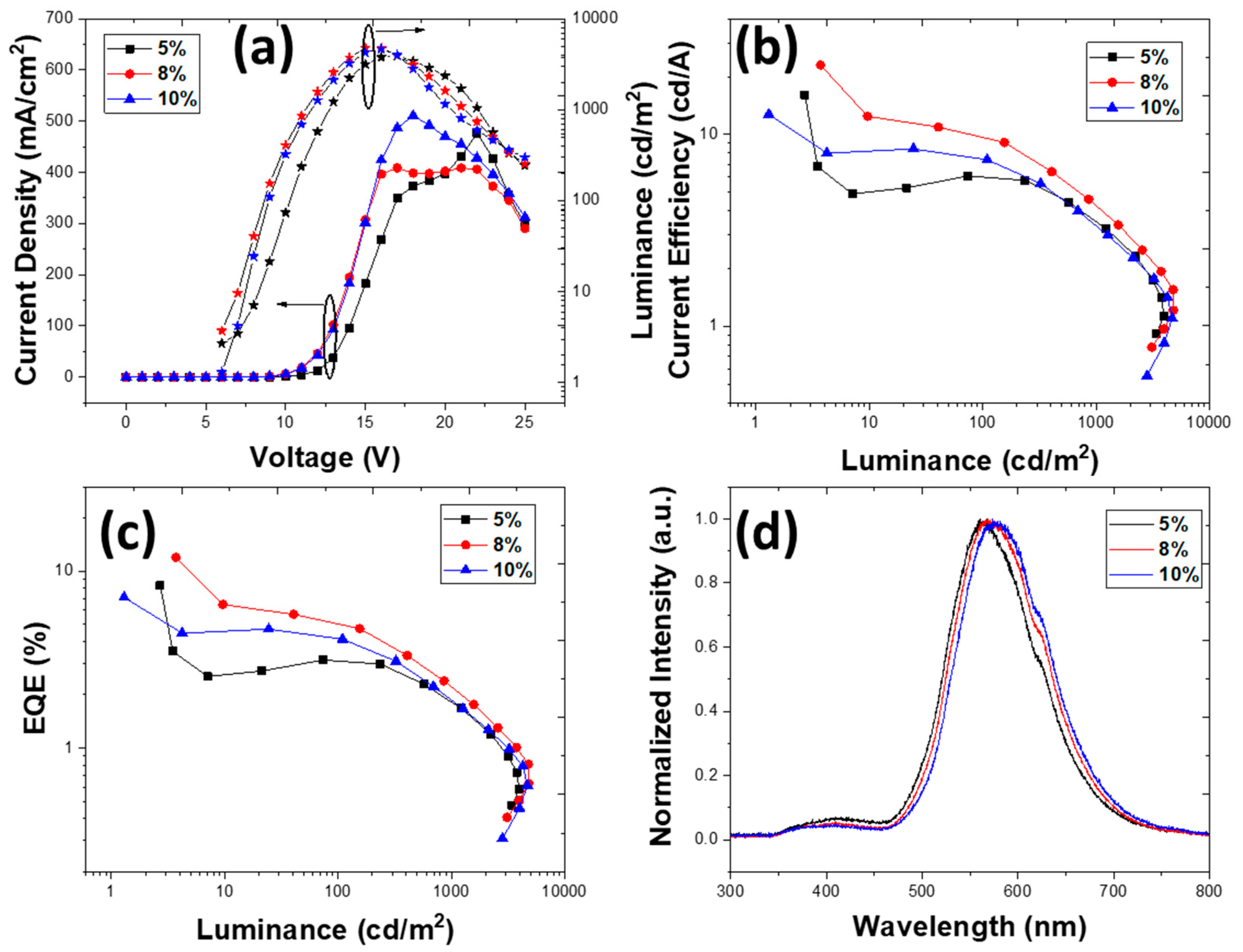
| 5 | 4.31 | 3.04 | 2.77 | 245 | 1.64 × 10⁻² | 14 | 0.43, 0.51 |
| 8 | 15.66 | 3.78 | 8.78 | 440 | 3.37 × 10⁻² | 13 | 0.50, 0.47 |
| 10 | 4.46 | 1.27 | 2.97 | 416 | 3.38 × 10⁻² | 11 | 0.50, 0.47 |
| EML thickness of 25 nm | |||||||
| 5 | 4.86 | 1.17 | 2.72 | 353 | 1.64 × 10⁻² | 13 | 0.43, 0.51 |
| 8 | 11.39 | 2.38 | 7.32 | 225 | 3.37 × 10⁻² | 13 | 0.50, 0.47 |
| 10 | 5.06 | 1.32 | 3.37 | 472 | 3.38 × 10⁻² | 12 | 0.50, 0.47 |
| TXO-TPA Wt.% | ηc (cd/A) | ηp (Lm/W) | EQE (%) | Lmax (cd/m2) | JON (mA/cm2) | VON (V) | CIE (x,y) |
|---|---|---|---|---|---|---|---|
| EML thickness of 40 nm | |||||||
| 5 | 4.15 | 2.17 | 2.00 | 3038 | 1.33 | 4 | 0.40, 0.53 |
| 8 | 5.52 | 3.46 | 2.71 | 3268 | 4.70 × 10⁻¹ | 4 | 0.43, 0.52 |
| 10 | 6.80 | 3.52 | 3.34 | 3279 | 1.76 | 4.5 | 0.44, 0.52 |
| EML thickness of 25 nm | |||||||
| 5 | 4.29 | 2.70 | 2.33 | 2939 | 2.28 | 4 | 0.40, 0.50 |
| 8 | 8.36 | 6.57 | 4.71 | 3115 | 9.0 × 10⁻² | 4 | 0.40, 0.48 |
| 10 | 9.00 | 7.07 | 5.47 | 3427 | 6.57 × 10⁻² | 4 | 0.40, 0.46 |
| Wt.% A = EML B = ETL | ηc (cd/A) | ηp (Lm/W) | EQE (%) | Lmax (cd/m2) | JON (mA/cm2) | VON (V) | CIE (x,y) |
|---|---|---|---|---|---|---|---|
| A = 25 nm, B = 40 nm | |||||||
| 5 | 21.00 | 9.42 | 10.39 | 3237 | 1.96 × 10⁻² | 6 | 0.44, 0.51 |
| 8 | 17.21 | 9.01 | 8.72 | 3878 | 2.53 × 10⁻² | 6 | 0.46, 0.50 |
| 10 | 10.95 | 7.95 | 7.99 | 3123 | 4.33 × 10⁻² | 6 | 0.47, 0.49 |
| A = 40 nm, B = 40 nm | |||||||
| 5 | 31.60 | 14.18 | 16.81 | 3180 | 3.75 × 10⁻² | 6 | 0.45, 0.51 |
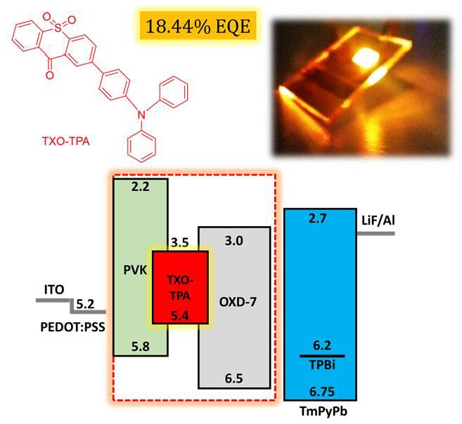
| 8 | 36.71 | 12.81 | 18.44 | 2585 | 3.11× 10⁻² | 6 | 0.48, 0.49 |
| 10 | 14.74 | 6.61 | 8.03 | 2992 | 2.37× 10⁻² | 6 | 0.49, 0.48 |
| A = 50 nm, B = 50 nm | |||||||
| 5 | 19.22 | 8.62 | 10.60 | 2240 | 1.90 × 10⁻² | 6 | 0.46, 0.50 |
| 8 | 29.24 | 13.12 | 15.33 | 1700 | 4.33 ×10⁻³ | 6 | 0.49, 0.48 |
| 10 | 6.14 | 4.36 | 6.14 | 2309 | 1.05 × 10⁻¹ | 6 | 0.49, 0.48 |
| A = 40 nm, B = 30 nm | |||||||
| 5 | 22.41 | 11.73 | 11.65 | 2885 | 8.90 × 10⁻³ | 6 | 0.44, 0.51 |
| 8 | 29.47 | 13.22 | 14.53 | 2513 | 5.57 × 10⁻³ | 6 | 0.47, 0.50 |
| 10 | 19.34 | 8.68 | 10.27 | 3021 | 2.11 × 10⁻² | 6 | 0.48, 0.49 |
| A = 40 nm, B = 50 nm | |||||||
| 5 | 26.21 | 11.76 | 13.73 | 1490 | 8.0 × 10⁻³ | 6 | 0.46, 0.50 |
| 8 | 28.60 | 14.97 | 15.82 | 3800 | 1.95 × 10⁻² | 6 | 0.49, 0.48 |
| 10 | 22.50 | 8.83 | 12.23 | 1922 | 2.04 × 10⁻² | 7 | 0.48, 0.49 |
| TXO-TPA Wt.% | ηc (cd/A) | ηp (Lm/W) | EQE (%) | Lmax (cd/m2) | JON (mA/cm2) | VON (V) | CIE (x,y) |
|---|---|---|---|---|---|---|---|
| 5 | 16.07 | 8.41 | 8.3 | 3950 | 1.67 × 10⁻² | 5.5 | 0.43, 0.50 |
| 8 | 22.97 | 12.02 | 11.95 | 4809 | 1.61 × 10⁻² | 5.5 | 0.46, 0.50 |
| 10 | 12.27 | 6.66 | 7.19 | 4681 | 1.02 × 10⁻² | 5.5 | 0.46, 0.51 |
© 2020 by the authors. Licensee MDPI, Basel, Switzerland. This article is an open access article distributed under the terms and conditions of the Creative Commons Attribution (CC BY) license (http://creativecommons.org/licenses/by/4.0/).
Share and Cite
Kumar, M.; Pereira, L. Towards Highly Efficient TADF Yellow-Red OLEDs Fabricated by Solution Deposition Methods: Critical Influence of the Active Layer Morphology. Nanomaterials 2020, 10, 101. https://doi.org/10.3390/nano10010101
Kumar M, Pereira L. Towards Highly Efficient TADF Yellow-Red OLEDs Fabricated by Solution Deposition Methods: Critical Influence of the Active Layer Morphology. Nanomaterials. 2020; 10(1):101. https://doi.org/10.3390/nano10010101
Chicago/Turabian StyleKumar, Manish, and Luiz Pereira. 2020. "Towards Highly Efficient TADF Yellow-Red OLEDs Fabricated by Solution Deposition Methods: Critical Influence of the Active Layer Morphology" Nanomaterials 10, no. 1: 101. https://doi.org/10.3390/nano10010101
APA StyleKumar, M., & Pereira, L. (2020). Towards Highly Efficient TADF Yellow-Red OLEDs Fabricated by Solution Deposition Methods: Critical Influence of the Active Layer Morphology. Nanomaterials, 10(1), 101. https://doi.org/10.3390/nano10010101