Article

TSRACE-AI: Traffic Sign Recognition Accelerated with Co-Designed Edge AI Based on Hybrid FPGA Architecture for ADAS

by
Abderrahmane Smaali
1,*,
Said Ben Alla
1 and
Abdellah Touhafi
2
1
LAVETE Laboratory, National School of Applied Sciences of Berrechid, University of Hassan I, Settat 26000, Morocco
2
Department of Engineering Sciences and Technology (INDI), Vrije Universiteit Brussel (VUB), 1050 Brussels, Belgium
*
Author to whom correspondence should be addressed.
Information 2025, 16(8), 703; https://doi.org/10.3390/info16080703
Submission received: 12 July 2025 / Revised: 15 August 2025 / Accepted: 16 August 2025 / Published: 18 August 2025

Abstract

The need for efficient and real-time traffic sign recognition has become increasingly important as autonomous vehicles and Advanced Driver Assistance Systems (ADASs) continue to evolve. This study introduces TSRACE-AI, a system that accelerates traffic sign recognition by combining hardware and software in a hybrid architecture deployed on the PYNQ-Z2 FPGA platform. The design employs the Deep Learning Processing Unit (DPU) for hardware acceleration and incorporates 8-bit fixed-point quantization to enhance the performance of the CNN model. The proposed system achieves a 98.85% reduction in latency and a 200.28% increase in throughput compared to similar works, with a trade-off of a 90.35% decrease in power efficiency. Despite this trade-off, the system excels in latency-sensitive applications, demonstrating its suitability for real-time decision-making. By balancing speed and power efficiency, TSRACE-AI offers a compelling solution for integrating traffic sign recognition into ADAS, paving the way for enhanced autonomous driving capabilities.

1. Introduction

The increasing demand for real-time processing in autonomous systems, particularly in Advanced Driver Assistance Systems (ADASs) [1] and autonomous vehicles [2], has driven significant advancements in both hardware and software design. These systems must meet stringent requirements for low latency and energy efficiency, which remain critical challenges in the field. Convolutional Neural Networks (CNNs) [3] have emerged as key enablers for achieving high accuracy in complex tasks such as traffic sign recognition. However, implementing CNNs on resource-constrained edge devices introduces challenges in balancing computational performance with energy efficiency. Addressing this balance is crucial for enabling real-time decision-making in autonomous systems.
Field Programmable Gate Arrays (FPGAs) have emerged as a promising solution for accelerating CNNs [4], particularly in environments with limited resources. Their exceptional versatility, combined with parallel processing capabilities and an energy-efficient architecture, ensures their suitability for edge AI applications [5]. Recent advancements in FPGA-based CNN accelerators [6] have focused on enhancing performance for real-time tasks. Research efforts have prioritized reducing power consumption while maintaining or improving computational throughput, making FPGAs increasingly practical for high-performance applications where speed and efficiency are paramount [7].
In this study, we present the design and implementation of a CNN-based system for real-time traffic sign recognition on an FPGA platform. Using the German Traffic Sign Recognition Benchmark (GTSRB) dataset [8], we focus on optimizing both detection [9] and classification tasks. Our solution is deployed on the PYNQ-Z2 platform and incorporates advanced techniques such as quantization, hardware–software partitioning, and pipeline optimization. These enhancements enable the system to achieve low latency and high throughput, meeting the rigorous demands of autonomous driving systems.
This work offers several key contributions. First, it demonstrates how CNN architectures can be effectively deployed on FPGA platforms for real-time traffic sign recognition. Second, our approach achieves a power efficiency of 4.96 GOPS/W and a throughput of 205.39 GOPS, contributing to advancements in FPGA-based accelerators for ADAS applications. Finally, the system’s low latency of 1.17 ms per inference highlights its suitability for safety-critical scenarios in intelligent transportation systems, where rapid and reliable decision-making is crucial.

2. Related Work

Edge computing and mobile devices demand solutions that balance real-time performance with energy efficiency, particularly in resource-constrained environments. Recent advancements in FPGA-based CNN acceleration have targeted these challenges, emphasizing the refinement of hardware–software integration to achieve substantial improvements in computational throughput while minimizing power consumption. These optimizations are pivotal for enabling deep learning applications in settings where efficiency and speed are critical.
Gundrapally et al. [10] introduced a high-performance, ultra-low-power accelerator for CNNs, specifically tailored for mobile FPGA platforms like the PYNQ-Z2. By optimizing the register transfer level (RTL) design, they achieved a 22% reduction in power consumption, significantly enhancing energy efficiency. The architecture demonstrated real-time capabilities by executing ResNet-20 [11] on the CIFAR-10 dataset [12], showcasing substantial improvements in both speed and energy usage. Their approach aligns closely with ongoing efforts to develop FPGA-based solutions for traffic sign recognition.
Doumet et al. [13] developed the H2PIPE architecture, exploiting high-bandwidth memory (HBM) on the Stratix 10 NX platform to accelerate CNNs. Their design achieved an impressive throughput of 4174 images per second and a computational performance of 15,109 GOPS, setting a new standard for power-efficient, real-time applications. This work underscores the critical role of maximizing throughput in large-scale CNNs and provides valuable insights for future hardware optimization efforts.
Gao et al. [14] proposed a 1D-CNN-Transformer architecture for radar emitter identification, implemented on Alveo U280 and PYNQ-Z2 platforms. Their FPGA-based accelerator improved latency, throughput, and adaptability across CNN layers, demonstrating its potential for flexible and scalable solutions in real-time object recognition tasks.
Trabelsi Ajili and Hara-Azumi [15] focused on a hybrid CPU-FPGA approach to accelerate DeepSense, a multimodal neural network designed for processing time-series data. By leveraging Xilinx Vitis AI and the Deep Learning Processing Unit (DPU), their solution achieved 2.5× lower latency and 5.2× energy savings compared to traditional software implementations, highlighting the suitability of FPGA accelerators for IoT and mobile platforms.
Mansouri et al. [16] combined CNNs and graph convolutional networks (GCNs) in a hybrid model for skeleton-based action recognition. Their FPGA implementation balanced accuracy with low-latency inference, making it suitable for real-time applications such as human–computer interaction and ADAS.
Wang et al. [17] developed a reconfigurable CNN-based system for object detection, utilizing FPGA pipeline architecture and off-chip memory to enhance computational efficiency. Tested on the Spartan-6 FPGA, their system achieved a detection speed of 16 FPS with a power consumption of only 0.79 W, representing a 178% improvement in speed over previous methods.
Yao et al. [18] enhanced CNN acceleration on the ZynqNet [19] platform using dynamic fixed-point quantization. Their system achieved a power efficiency of 5.24 GOPS/W, demonstrating the feasibility of FPGA accelerators for IoT and mobile applications.
Kim et al. [20] proposed a fully integer-based CNN accelerator implemented on a Xilinx ZC706 FPGA for real-time traffic sign recognition (TSR). Their architecture employs quantization-aware training (QAT) and a hardware-friendly quantization method (LLTQ), enabling all operations including skip connections in residual blocks to be performed using only integer arithmetic. The proposed design achieved a frame rate of 40 FPS, with a compact model size of 0.17 MB, and required 24 million integer operations (IOPs). The system delivered 960 MOPS computation performance and 99.07% accuracy on the GTSRB dataset. Furthermore, the authors optimized both residual block dataflow and internal memory utilization to meet the stringent resource constraints of embedded platforms.
Tatar and Bayar [21] proposed a real-time multi-task ADAS system implemented on a Xilinx Kria KV260 MPSoC platform. Their system executes multiple ADAS tasks simultaneously including semantic segmentation, object detection, lane detection, and drivable area recognition using a shared ResNet-18 backbone and an SSD detection subnet. To achieve real-time performance on resource-constrained hardware, they employed quantization-aware training to compress the model to 8-bit integer precision, along with software–hardware co-design strategies (Vitis-AI, AXI-DMA interfacing). The implementation reached 25.4 FPS at 1080p resolution, while maintaining competitive accuracy across all tasks (e.g., 56.62% mIoU for segmentation and 81.56% IoU for drivable area recognition).
Xilinx’s ResNet50-PYNQ project [22] demonstrates a fully quantized, dataflow-style accelerator for ResNet-50 controlled from Python 3.6 via PYNQ. Unlike a general-purpose DPU overlay, the design is compiled for a single network and emphasizes aggressive on-chip buffering and inter-layer streaming to minimize off-chip memory traffic. As a result, it serves both as a canonical dataflow baseline and a host-control reference point: the pipeline trades flexibility for locality and steady-state throughput, offering a useful contrast to overlay-based deployments.
Nguyen and Nakashima [23] studied a multi-core CNN accelerator on an Alveo U280 with HBM2 and provided a clean comparison against DDR using the same compute engine. They reported about 912.7 GOPS and 22.48 GOPS/W on VGG-16, with tiny image latency near 0.704 ms for 3 × 32 × 32 inputs, attributing the gains to HBM port partitioning, double buffering, and long AXI bursts that raise effective bandwidth. This work highlights how, once arithmetic throughput is sufficient, the memory system (HBM2 vs. DDR) becomes the dominant factor in end-to-end performance.
Finally, Han and Oruklu [24] presented an FPGA-based system for real-time traffic sign recognition, integrating the Zynq-7000 FPGA with ARM SoCs. Their method combined hue detection and template matching using Hausdorff distance calculations, achieving an 8× speed improvement over earlier implementations. This work underscores the potential of FPGA-based systems for intelligent transportation applications.

3. Design Approach

This study presents a hybrid CPU-FPGA hardware/software co-design aimed at accelerating a deep convolutional neural network (DCNN) model for traffic sign recognition (TSR). The approach utilizes the Xilinx DNNDK framework [25] and the Deep Learning Processing Unit (DPU) [26] accelerator to enhance the performance and efficiency of the TSR system. Based on a detailed analysis of the DCNN workload [27], the design targets low-latency and energy-efficient deployment suitable for constrained edge computing platforms such as the PYNQ-Z2.
The TSR system was implemented on the PYNQ-Z2 board following a structured three-phase development methodology, consisting of software, hardware, and hardware–software co-design. As shown in Figure 1, the workflow begins with training and evaluating a DCNN model using the GTSRB dataset. After training, the model is converted into a frozen graph, which is a computation graph where all variables are converted into fixed constants. This format simplifies the model and prepares it for deployment. The frozen graph is then quantized, converting floating-point parameters into fixed-point (typically 8-bit) representations.
Next, the quantized graph and the hardware description file (HDF) generated by Vivado are provided as inputs to the compilation stage. In this phase, the DNNDK compiler generates executable binaries for the DPU architecture. One of these outputs is labeled as DPU ADAS, indicating that the binary is prepared for real-time traffic sign inference tasks within advanced driver-assistance systems. This output contains the optimized graph representation that the DPU will execute at runtime.
Simultaneously, the hardware components defined in Vivado are used to generate a programmable logic bitstream. The Petalinux project build process then combines this bitstream with additional runtime components, device drivers, libraries, and system services. The result of this build process is a fully configured embedded operating system that runs on the ARM Cortex-A9 processor. In Figure 1, the arrow from project build to operating system reflects this integration, showing that the build process generates the system software environment required for the deployed application to function correctly on the FPGA board.
This workflow ensures an efficient mapping of neural network workloads onto the FPGA fabric, combining software flexibility with hardware acceleration. The result is a compact, high-performance TSR system optimized for real-time execution in edge applications such as autonomous driving.

3.1. Phase 1: Software Preprocessing and Model Training

The initial phase of the project involved setting up the software environment, focusing on data preprocessing and model training to facilitate seamless integration with the DNNDK framework. This phase established the foundation for optimizing inference performance on FPGA hardware. Key steps included:
  • Model Adjustment: The neural network architecture was tailored to align with the constraints and capabilities of the DNNDK framework, ensuring compatibility with the DPU for hardware acceleration. This involved optimizing the model’s structure to minimize computational overhead and enhance execution efficiency. Various data augmentation techniques, including random rotations, scaling, and flipping, were applied to improve the model’s robustness. These augmentations enabled the model to generalize effectively, preparing it for real-world conditions.
  • Preprocessing: Extensive preprocessing was conducted to standardize the input data. The GTSRB dataset, containing traffic sign images of varying sizes and lighting conditions, was resized to uniform dimensions of 32 × 32 × 3. Pixel normalization was applied to scale values, facilitating faster convergence during training. These preprocessing steps ensured uniformity and enhanced the model’s ability to handle data efficiently in both software and hardware environments.
  • Network Training: The adjusted model was trained using the preprocessed GTSRB dataset. Key performance indicators such as accuracy, precision, recall, and loss were closely monitored to guide model fine-tuning. Optimization techniques, including learning rate scheduling, Adam optimizer, and dropout, were employed to mitigate overfitting and accelerate convergence. The training process involved multiple iterative experiments to achieve optimal performance while maintaining compatibility with the DNNDK environment.
  • Evaluation: The trained model was rigorously evaluated across various metrics, including accuracy, precision, recall, and F1-score, to confirm its suitability for real-time traffic sign recognition. Inference latency tests were also conducted within the DNNDK framework to assess the model’s efficiency when deployed on FPGA hardware. The design emphasized balancing computational efficiency and accuracy, ensuring the model’s readiness for deployment in resource-constrained environments such as mobile devices and automotive applications.

3.1.1. Model Architecture and Training

This study focuses on developing and evaluating a DCNN designed for Traffic Sign Recognition (TSR) using the GTSRB dataset. The model’s architecture is specifically designed to efficiently process and extract features from input images of size 32 × 32 × 3, making it suitable for deployment on resource-constrained hardware platforms.
Model Architecture
The DCNN used in this study comprises multiple convolutional, pooling, dropout, and fully connected layers, as detailed in Table 1:
Table 1 presents the detailed layer-wise computational complexity and parameter summary of the proposed TSRACE-AI model. The model is composed of four convolutional layers, each followed by activation functions and pooling/dropout operations to ensure spatial feature extraction, regularization, and dimensionality reduction. The total number of trainable parameters is approximately 357 K, with a total of 242.48 million operations, highlighting the model’s efficiency for deployment on resource-constrained edge platforms such as the PYNQ-Z2. Despite its lightweight architecture, TSRACE-AI maintains strong representational capability, making it suitable for real-time traffic sign recognition tasks in ADAS applications.
Explanation of Layers
Input Layer: Accepts input images of size 32 × 32 × 3, where the third dimension corresponds to RGB color channels. The choice of 32 × 32 resolution follows the GTSRB benchmark preprocessing standard, which ensures a fixed-size input for consistent training while preserving sufficient visual detail for classification. Smaller sizes (e.g., 24 × 24) risk losing discriminative features of complex signs, whereas larger sizes (e.g., 64 × 64) increase computational load and latency, making real-time FPGA deployment less feasible.
Conv2D Layers (Layer 1 to Layer 4): Extract features such as edges, textures, and patterns through 2D convolution operations. In our design, the kernel sizes are: Layer 1: 5 × 5, Layer 2: 5 × 5, Layer 3: 3 × 3, Layer 4: 3 × 3. Mathematically, the convolution operation between an image I and kernel K is defined as follows [28]:
( I K ) ( x , y ) = i = 0 k 1 j = 0 k 1 I ( x + i , y + j ) · K ( i , j )
where I ( x , y ) represents the pixel value of the input image at coordinates ( x , y ) , and K ( i , j ) represents the kernel value at position ( i , j ) . This operation slides the kernel K over the image I, applying a weighted sum of the kernel values to the local region of the image, thereby extracting relevant features such as edges and textures. This process helps in feature extraction, which is essential for higher-level tasks like classification.
MaxPooling2D Layers: These layers reduce the spatial dimensions (height and width) of the feature maps by selecting the maximum value from non-overlapping regions, improving computational efficiency and reducing overfitting. In this case, pooling is applied with a stride of 2.
Dropout Layers: These layers introduce random deactivation of neurons during training, which helps prevent overfitting and improves the model’s ability to generalize to unseen data. In this model, a dropout rate of 50% was applied, meaning half of the neurons were randomly deactivated at each training step.
Flatten Layer: Converts the 4-dimensional tensor output from the convolutional layers into a 1-dimensional vector, preparing it for the fully connected (dense) layers.
Dense Layers (Layer 5 and Output): Fully connected layers that map the extracted features into class probabilities. The dense layer applies the following operation:
z = W x + b
where W represents the weights matrix, x is the input, and b is the bias term. The dense layer with 256 units is followed by the output layer, which uses a SoftMax activation function to generate probabilities for the 43 traffic sign classes, corresponding to the number of distinct traffic sign categories in the GTSRB dataset.
Model Training Process
The TSRACE-AI model was trained on the GTSRB dataset, consisting of over 50,000 images across 43 traffic sign classes. The dataset was split into 70% for training, 15% for validation, and 15% for testing, using a stratified split per class with a fixed random seed to ensure reproducibility. This approach guaranteed a balanced representation across all classes, while the held-out test set was used solely for final performance evaluation. Training involved extensive performance monitoring using metrics such as accuracy, precision, recall, and F1-score. Optimization techniques, including learning rate scheduling, the Adam optimizer, and dropout, were applied to accelerate convergence and prevent overfitting. The model was trained for a total of 30 epochs with a batch size of 32 and an initial learning rate of 0.001. Rectified Linear Unit (ReLU) activation functions were applied to all convolutional and dense layers, except for the final output layer, which used a softmax activation to handle the 43-class classification task. This configuration ensured robust and efficient performance suitable for deployment on FPGA hardware.
Key Stages of the Training Process:
  • Preprocessing: All images were resized to 32 × 32 pixels, normalized to the range [0, 1], and augmented with techniques such as horizontal flipping, rotation, zooming, random shifts, and brightness adjustments. These techniques improved the model’s generalization ability and helped prevent overfitting by exposing it to a more diverse set of input conditions. Data preprocessing and augmentation were implemented during training using the ImageDataGenerator pipeline in Keras.
  • Loss Function: The model’s predictions were evaluated using the categorical cross-entropy loss function, defined as follows:
    L = i = 1 N y i log ( y ^ i )
    y i denotes the true label, while y ^ i represents the predicted probability for the corresponding class.
    Optimization: The Adam optimizer was utilized to minimize the loss function with an initial learning rate of 0.001, which was linearly decayed to 0.00005 over the 30 training epochs. This algorithm adaptively adjusts the learning rates for individual parameters by computing moving averages of the gradients and their squared values, thereby accelerating convergence. The update rules are given as follows [29]:
    m t = β 1 m t 1 + ( 1 β 1 ) t
    v t = β 2 v t 1 + ( 1 β 2 ) t 2
    where t represents the gradient at time step t, and m t and v t denote the first and second moment estimates, respectively. The hyperparameters β 1 and β 2 , which control the exponential moving averages of the gradient and its square, were fixed at their default values of 0.9 and 0.999 throughout the training process.

3.1.2. Evaluation and Results

The model was evaluated on the GTSRB dataset, which comprises 43 distinct traffic sign classes. The evaluation metrics and visualizations confirmed the model’s robustness, demonstrating its potential for real-world applications in autonomous driving and ADAS.
Model Accuracy and Loss
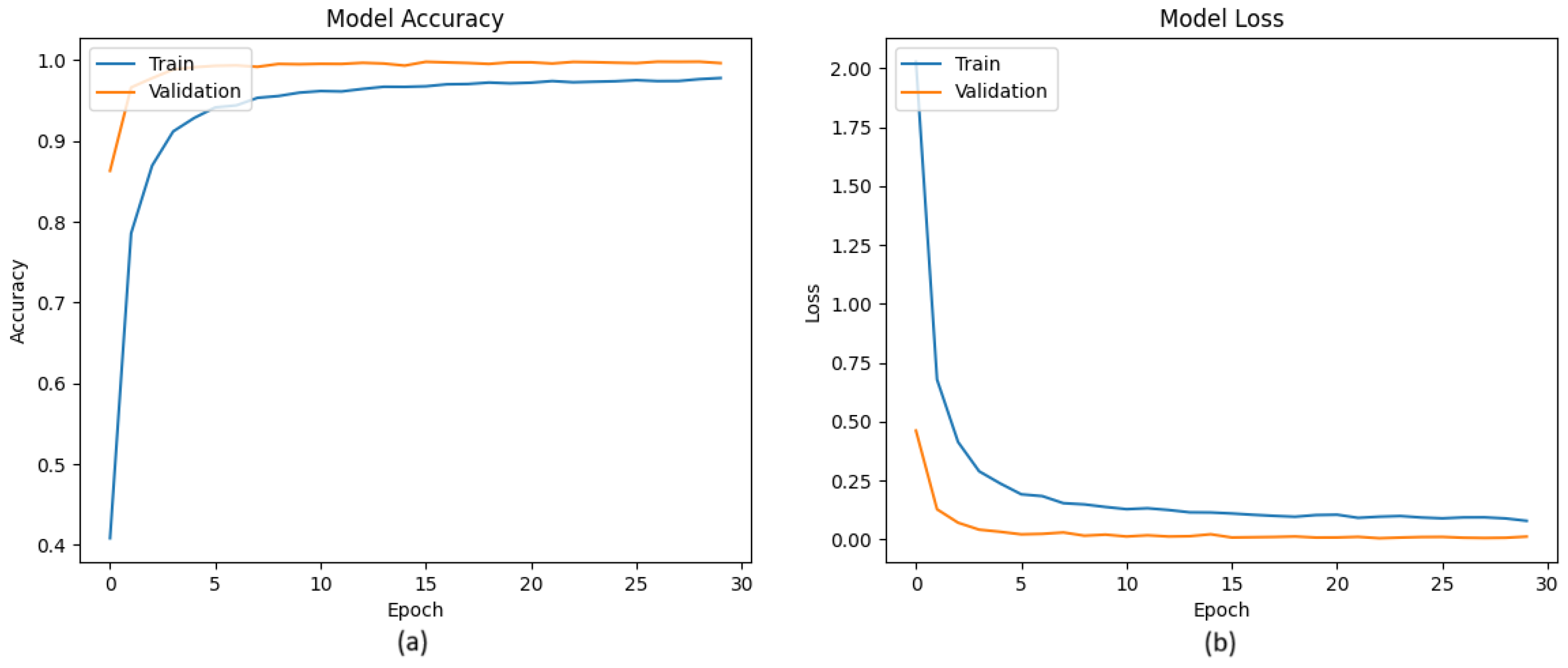
The performance of the TSRACE-AI model was evaluated by monitoring its accuracy and loss over 30 training epochs. As illustrated in Figure 2, the training and validation curves provide clear insight into the learning dynamics and generalization behavior of the network.
During training, the learning rate decreased linearly from 0.001 to 0.00005, as shown in Figure 2. At the end of the 30 epochs, the TSRACE-AI model achieved a training accuracy of 98.7% and a validation accuracy of 96.4%, with corresponding final training and validation losses of 0.021 and 0.087, respectively.
Accuracy: The model’s accuracy on both the training and validation sets increased sharply during the initial 10 epochs, ultimately stabilizing near 1.0. This indicates a strong ability of the network to learn distinguishing features without significant overfitting.
Loss: The training and validation loss values dropped rapidly during early epochs and converged to low values, demonstrating effective optimization and smooth convergence of the learning algorithm.
Overall, these results confirm that the TSRACE-AI model achieves excellent generalization on unseen data, maintaining a strong trade-off between learning performance and model stability.
Confusion Matrix
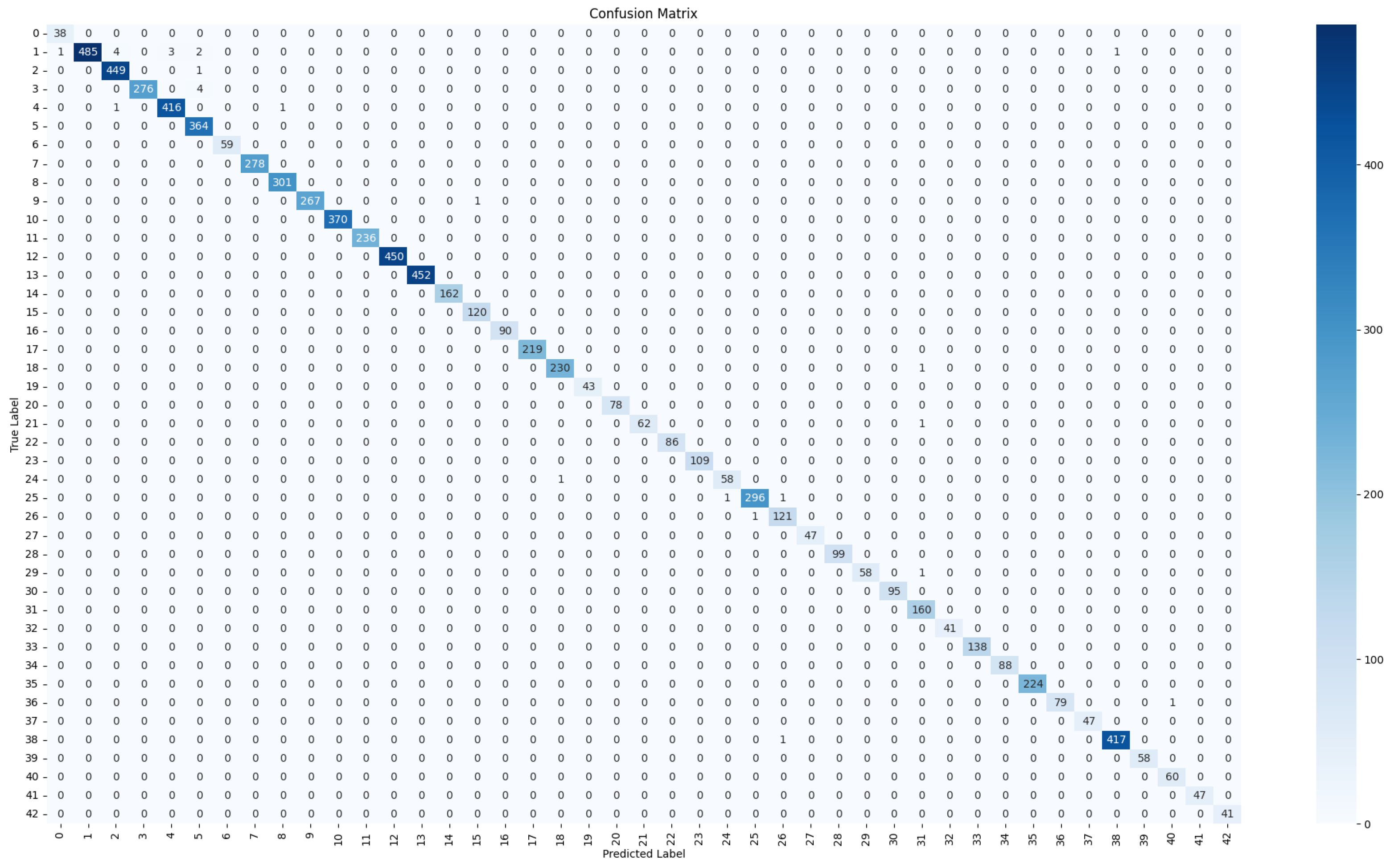
The confusion matrix, shown in Figure 3, offers a comprehensive analysis of the model’s classification performance across the 43 traffic sign classes. Key observations include:
  • High Accuracy: The model exhibits strong classification performance across most classes, with very few misclassifications.
  • Misclassification Patterns: Errors, though rare, primarily occur between visually similar traffic signs, highlighting areas for potential refinement.
  • Diagonal Dominance: The high concentration along the diagonal reflects a significant proportion of correct predictions, confirming the robustness of the training process.
Minimal off-diagonal values underscore the model’s suitability for high-precision applications, such as autonomous driving. This evaluation reinforces the model’s reliability in detecting and classifying traffic signs, establishing its readiness for deployment in real-world edge AI systems.
Evaluation Metrics
To thoroughly evaluate the model’s performance, precision, recall, and F1-score were calculated based on its predictions on the test set. These metrics are defined as follows:
Precision = TP TP + FP = 0.9965
Recall = TP TP + FN = 0.9664
F1-score = 2 · Precision · Recall Precision + Recall = 0.9812
where:
  • TP (True Positives): The number of correctly predicted samples for a given class, represented by the value on the main diagonal of the confusion matrix in Figure 3.
  • FP (False Positives): For a given class, these are the samples incorrectly predicted as belonging to that class. In the confusion matrix, FP for a specific class is the sum of the corresponding column values excluding the diagonal element.
  • FN (False Negatives): For a given class, these are the samples from that class that were incorrectly predicted as another class. In the confusion matrix, FN for a specific class is the sum of the corresponding row values excluding the diagonal element.
For example, in Figure 3, if we examine class label 0:
  • TP = 485 (main diagonal value at row 0, column 0)
  • FP = sum of all values in column 0 except row 0 (e.g., 0 from row 1, 0 from row 2, etc.)
  • FN = sum of all values in row 0 except column 0 (e.g., 3 from column 1, 0 from column 2, etc.)
These high precision, recall, and F1-score values indicate the model’s strong ability to classify traffic signs accurately, with minimal false positives and false negatives. Such performance is crucial for real-time applications in autonomous driving, where reliable traffic sign recognition is vital.
Misclassification Analysis
The proposed TSRACE-AI model was intentionally designed with a compact four-layer CNN to satisfy strict real-time constraints on resource-limited FPGA hardware while still achieving high accuracy on clean and moderately altered inputs. Despite its reduced depth, the network successfully captured a wide range of patterns. To address complex visual conditions, a data augmentation pipeline was implemented, incorporating brightness and contrast variations alongside geometric transformations (rotation, zoom, shift, shear) to improve generalization to low-light, shadowed, or visually distorted traffic signs. A detailed misclassification analysis was performed to further assess model behavior. Figure 4 illustrates representative cases of the TSRACE-AI model’s predictions, including both classified traffic signs (green annotations) and misclassified cases (red annotations). This analysis provides insight into the model’s strengths and limitations.
Correctly classified examples demonstrate robustness to variations in lighting, perspective, and partial occlusion, confirming the effectiveness of the augmentation strategy. However, misclassified cases reveal the model’s limitations, with most errors linked to substantial noise, low visibility, or unusual viewing angles; conditions that are challenging even for human recognition.
To improve robustness, future work will investigate training on more diverse datasets (e.g., GTSRB-Real, simulated fog/night conditions) and incorporating attention-based mechanisms or lightweight residual blocks while ensuring deployment feasibility on low-power edge devices.

3.1.3. Software Phase Outcome

The completion of the software phase marked a significant milestone in the development of the TSRACE-AI system. By integrating preprocessing, data augmentation, and model optimization, the system achieved high accuracy and minimized overfitting. Performance metrics, including accuracy, loss, and inference latency, confirmed the model’s readiness for deployment.
With the software phase successfully completed, the next step involves transitioning to the hardware (HW) phase. This phase focuses on deploying the optimized CNN model onto the FPGA platform for hardware acceleration. By integrating hardware-specific optimizations such as quantization and pipeline design, the TSRACE-AI system aims to further reduce latency and enhance throughput, ensuring it meets the stringent real-time demands of autonomous driving applications.

3.2. Phase 2: Hardware Process

The hardware design phase played a pivotal role in meeting the performance and efficiency targets of the TSRACE-AI system. Given the critical requirements for real-time processing and low-latency inference, we adopted an FPGA-based implementation on the Xilinx Zynq-7000 SoC platform. This platform combines the flexibility of software with the computational efficiency of hardware acceleration, making it ideal for deploying deep learning models in resource-constrained environments.
The primary objective of this phase was to integrate the Deep Learning Processing Unit (DPU) with the Zynq Processing System (PS) and optimize communication between them. This integration was key to achieving high-throughput inference while maintaining minimal latency.

3.2.1. Overview of Zynq Architecture

The Xilinx Zynq-7000 SoC is a hybrid architecture that integrates a dual-core ARM Cortex-A9 Processing System (PS) with programmable logic (PL) on a single chip. This architecture enables the execution of complex software algorithms on the ARM cores while offloading computationally intensive tasks, such as convolutional operations in deep learning, to the programmable logic. By using this hybrid approach, the Zynq platform offers significant improvements in efficiency and performance, making it a suitable choice for real-time traffic sign recognition in autonomous systems.
Key Advantages of This Architecture:
  • Hardware–Software Co-Design: The Zynq SoC facilitates a seamless co-design approach, enabling software and hardware to work in tandem. The ARM cores handle control flow and lighter computational tasks, while the FPGA’s programmable logic accelerates compute-intensive operations like matrix multiplications and convolutions.
  • Efficient Resource Utilization: By using both the processing system (PS) and programmable logic (PL), the Zynq platform maximizes resource efficiency, significantly enhancing performance while maintaining design flexibility.
  • Low Power and High Performance: The PL is optimized for power-efficient deep learning computations, making it ideal for resource-constrained applications, including Advanced Driver Assistance Systems (ADASs) and Edge AI solutions.
The ability of the Zynq-7000 SoC to offload deep learning tasks to the FPGA’s programmable logic while reserving the ARM cores for control tasks offers substantial advantages in power efficiency and performance. These features make the Zynq platform particularly suited for real-time applications in environments with constrained resources, such as autonomous vehicles and Edge AI systems.

3.2.2. DPU and DNNDK Integration

The Xilinx Deep Learning Processing Unit (DPU) is a specialized IP core designed for the efficient execution of deep convolutional neural networks (DCNNs). Supporting a wide range of neural network architectures, including VGG [30], ResNet, and MobileNet [31], the DPU is particularly well-suited for deployment in embedded systems based on FPGA technology. As shown in Figure 5, the DPU architecture includes a hybrid computing array of processing elements (PEs), a high-performance scheduler, a global memory pool, and an instruction fetch unit. These components operate together to enable high-throughput and low-latency inference on quantized models.
In this study, the deployed DPU utilized both on-chip BRAM and off-chip DDR memory to optimize memory access latency and throughput. The PYNQ-Z2 board is based on the Xilinx Zynq-7020 SoC (XC7Z020-1CLG400C), which integrates a dual-core ARM Cortex-A9 Application Processing Unit (APU) with FPGA Programmable Logic (PL). The board provides 512 MB DDR3 memory (16-bit bus @ 1050 Mbps), primarily used to store large data such as input images, intermediate feature maps, and trained model parameters. Meanwhile, the PL fabric contains 140 BRAM tiles (13.1 Mb, ≈630 KB on-chip), used for latency-critical data such as instruction buffers, control signals, and temporary tiles of feature maps and weights during convolution execution.
Data transfer between DDR and BRAM is handled by the High-Speed Data Tube, leveraging the AXI interface for efficient memory access. During inference, image data and model parameters are fetched from DDR into BRAM via DMA. The Instruction Fetch Unit schedules execution, and the High-Performance Scheduler assigns operations to the PEs inside the Hybrid Computing Array. Intermediate results are cached in BRAM to minimize latency before final outputs are written back to DDR. This memory hierarchy is essential for sustaining real-time traffic sign recognition performance.
The DPU operates in close coordination with the APU, which runs PetaLinux, manages task scheduling, initiates inference via the DNNDK runtime, and performs preprocessing (resizing, normalization) and post-processing (e.g., softmax classification).
For deployment, we used the DPUCZDX8G IP (DPU v3.0) from the Xilinx DNNDK toolkit. The chosen configuration, summarized in Table 2, was B1152 with Low RAM usage mode and Low DSP usage mode. This architecture executes up to 1152 MAC operations per clock cycle, balancing computational throughput with the Zynq-7020’s limited resources.
Only one DPU core was instantiated, as adding a second core would exceed available BRAM and DSP resources. In Low RAM usage mode, BRAM consumption is 123 blocks (87.86% of total), compared to 145 in High RAM mode. Low DSP usage mode limits DSP utilization to 146 slices (66.36%), with multiplications handled by DSP48 units and accumulations in LUTs to preserve DSP headroom. LUT usage reaches 35,280 (66.3%) and FF usage 49,860 (46.9%), staying within device limits. These figures are consistent with the utilization report in Section 4.1, confirming the configuration’s compatibility with the hardware.
The extra operations listed in this configuration, ElementwiseAdd and LeakyReLU, are both natively supported by the DPUCZDX8G IP [32], as confirmed by the official product guide (PG338). LeakyReLU is implemented directly in hardware along with other activation functions such as ReLU, ReLU6, Hard Sigmoid, and Hard Swish. Similarly, Elementwise operations, including Elementwise-sum (Add) and Elementwise-multiply, are supported and executed by the DPU without requiring fallback to the CPU.
This configuration represents an optimized trade-off between throughput, latency, and resource usage, enabling real-time inference within the constraints of the PYNQ-Z2 hardware platform.

3.2.3. Hardware Design Workflow

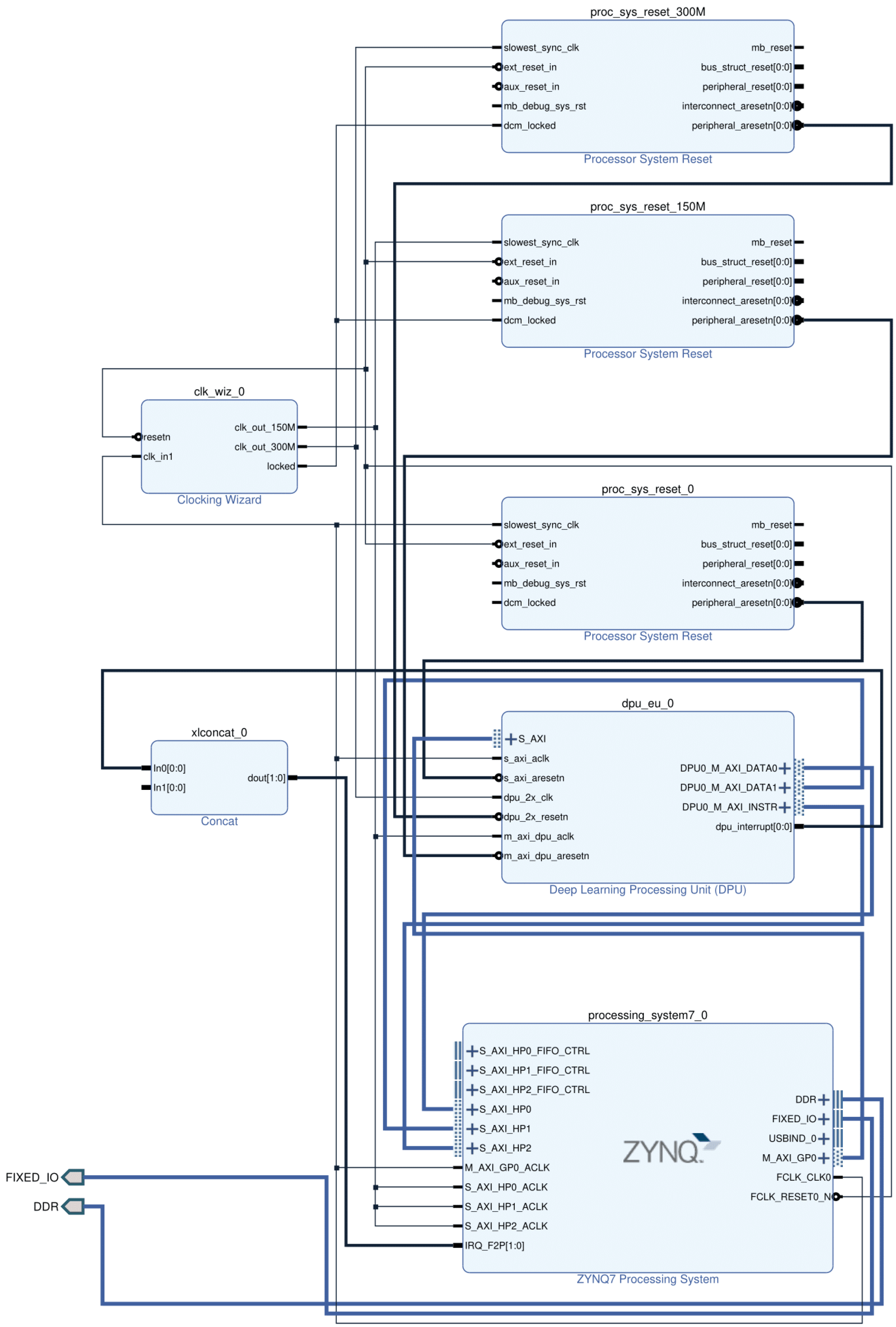
Figure 6 illustrates the block design used for integrating the Deep Learning Processing Unit (DPU) onto the Zynq platform, using the Vivado design environment. The design connects the Processing System (PS), which contains the ARM processor, to the Programmable Logic (PL), where the DPU is instantiated, enabling hardware acceleration for deep learning inference.
The processing system block includes the ARM Cortex-A9 dual-core processor, which runs a Linux-based operating system and manages high-level control tasks. It initiates inference operations and communicates with the DPU through high-speed AXI interfaces to transfer weights, input data, and retrieve inference results from DDR memory.
The dpu block represents the instantiated DPUCZDX8G IP core. This unit performs most of the deep learning computations, such as convolutions, activations, and pooling operations. The DPU communicates with memory using AXI master interfaces and executes CNN layers after receiving a start command from the processor.
A Clocking Wizard IP core (clk_wiz) was configured to generate two essential clock domains: a 150 MHz clock (clk_out1) used for AXI interconnects, control logic, and processor-side peripherals, and a 300 MHz clock (clk_out2) dedicated to driving the DPU core. These two clock signals operate in separate domains, introducing the need for proper synchronization and reset handling to ensure robust and error-free data transfer.
In systems involving multiple clock domains, improper synchronization can lead to metastability issues, data corruption, or unpredictable logic behavior during clock domain crossings (CDCs). This risk is particularly critical in DPU-based architectures where high-throughput AXI interfaces (e.g., S_AXI_ACLK, dpu_2x_clk) continuously transfer data between the PS and PL subsystems running at different frequencies. Without proper reset synchronization, asynchronous signals propagating between domains can cause timing violations or corrupted transactions.
To prevent such hazards, the design incorporates multiple proc_sys_reset blocks, each associated with a specific clock domain (150 MHz, 300 MHz, or FCLK_CLK0). These blocks generate synchronized, glitch-free reset signals for all modules operating under their respective clocks. For example, proc_sys_reset_150M manages resets for AXI and control peripherals, while proc_sys_reset_300M handles the DPU’s high-speed core. The reset polarity was set to active-low, ensuring that resets are asserted during power-up or reconfiguration and only deasserted once the associated clock is stable, as confirmed by the locked signal from the Clock Wizard.
This synchronized reset strategy ensures:
  • Clean startup behavior across all clock regions,
  • Safe transition of control and data signals between PS and PL,
  • Reliable handshaking over AXI interfaces (M_AXI_INSTR, M_AXI_DATA0, M_AXI_ DATA1),
  • Glitch-free operation, even during partial reconfiguration or low-power modes.
AXI interconnects serve as the communication bridge between the PS and PL, allowing the DPU to fetch input data and weights directly from shared DDR memory. Once the DPU receives a start command, it autonomously processes the CNN model and writes the final output back to memory.
In cases where a layer such as ElementwiseAdd is not supported by the DPU hardware, the DNNDK runtime automatically redirects the computation to the ARM processor. In contrast, supported layers like LeakyReLU are executed directly on the DPU, as documented in the official product guide.
The DPU also generates interrupts (dpu_interrupt and sm_interrupt) to notify the processor of task completion, enabling asynchronous and event-driven control of the inference workflow.
To enhance memory throughput, the AXI address space was manually configured with a non-overlapping memory map for each peripheral. This mapping ensures efficient access to both instructions and data and minimizes contention. These design elements collectively ensure the stability, reliability, and performance required for real-time TSRACE-AI operation on the Xilinx Zynq-7020 SoC (XC7Z020-1CLG400C).

3.2.4. Hardware Phase Outcome

The hardware design phase successfully met the performance and latency objectives of the TSRACE-AI system. Taking advantage of the PYNQ-Z2 FPGA platform and integrating the DPU enabled high-throughput and low-latency inference, making the system highly effective for real-time traffic sign recognition in ADAS. Efficient utilization of the Zynq-7000 SoC’s programmable logic for compute-intensive tasks, alongside the flexibility of the ARM cores for control operations, demonstrated the advantages of FPGA-based implementations in resource-constrained environments.
The implementation of the Xilinx DNNDK toolkit for quantization and model optimization further ensured that both performance and power efficiency targets were achieved, solidifying the system’s suitability for real-time edge AI applications.

3.3. Phase 3: HW/SW Co-Design

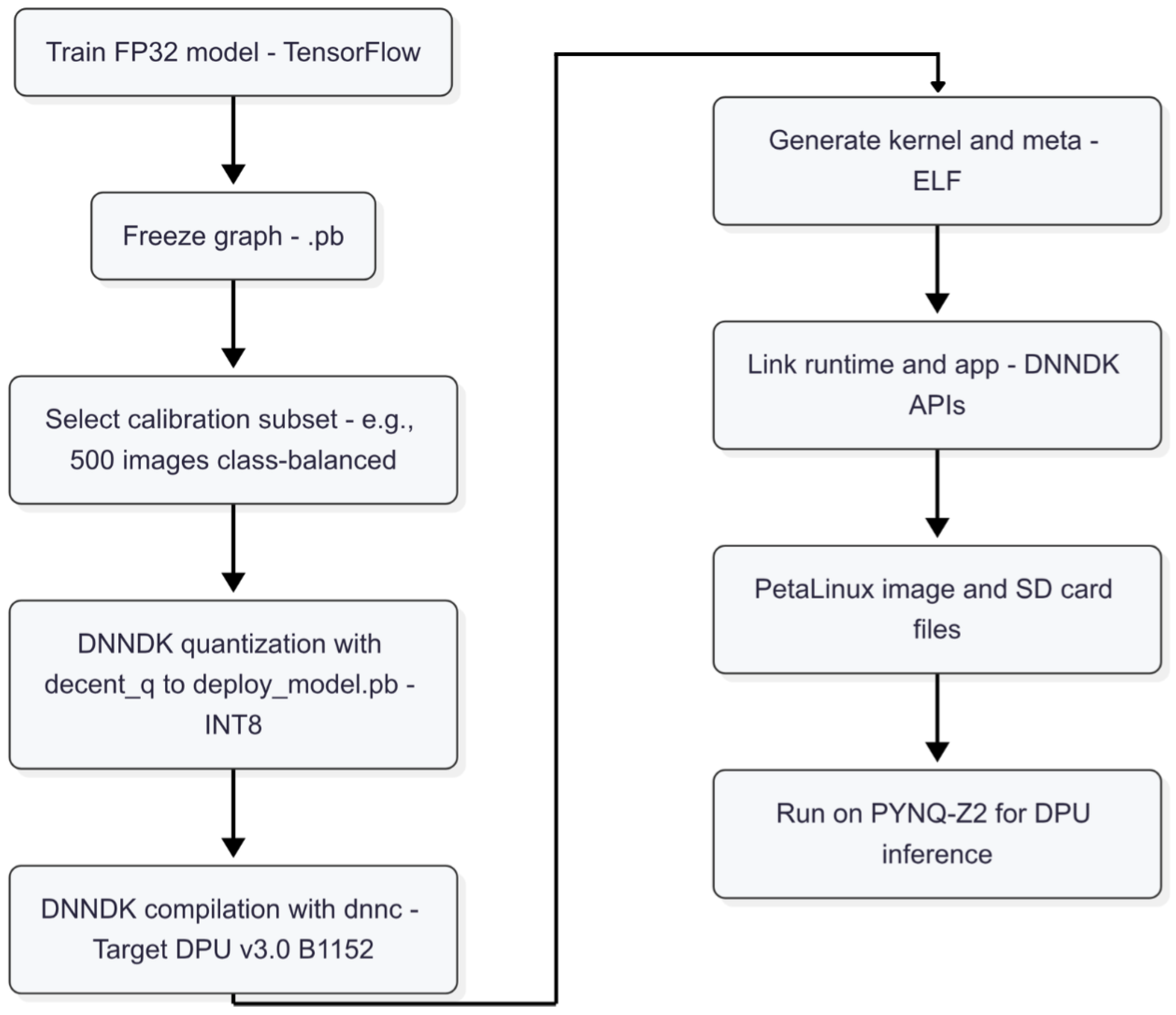
The HW/SW co-design phase was instrumental in creating an efficient and scalable TSR system on the PYNQ-Z2 platform. To clearly illustrate the development process, Figure 7 presents the DNNDK-based design flow, showing the key steps from FP32 model training, INT8 quantization, and DPU compilation, to packaging and deployment on the target FPGA.
By seamlessly integrating hardware and software components, TSRACE-AI effectively balances computational workloads between the CPU and FPGA. This hybrid approach relies on the strengths of both architectures to optimize performance and power efficiency, meeting the rigorous demands of real-time autonomous driving systems. Furthermore, TSRACE-AI achieves these advancements while maintaining low power consumption—a critical requirement for resource-constrained environments such as edge AI applications. The successful implementation of TSRACE-AI underscores the potential of FPGA-based co-design for high-performance, energy-efficient solutions in ADAS and similar domains.

3.3.1. Quantization and Compilation

Quantization of the trained neural network model was the first critical step in the HW/SW co-design phase. Using the Xilinx DNNDK framework, the original 32-bit floating-point model trained in TensorFlow was converted into an 8-bit fixed-point format, significantly reducing memory footprint and computational complexity.
Quantization Process:
  • Model Adjustment: The network architecture was adapted to ensure compatibility with the DPU, addressing unsupported layers and optimizing for the 8-bit fixed-point format. Adjustments were made to ensure that all layers and operations complied with the DNNDK’s supported layer types, and that quantization could be applied effectively across the model.
  • Calibration: A subset of 500 images from the training dataset was used to calibrate the quantized model. These images were randomly and uniformly sampled across all 43 classes to ensure balanced representation of traffic sign types. The calibration process was conducted using the DNNDK quantization tool (decent_q), which collected statistical activation data (min, max, histogram) during forward passes through the floating-point model. This enabled the computation of appropriate quantization parameters such as scale and zero-point, ensuring minimal performance degradation compared to the original floating-point version.
Once quantization was complete, the DNNDK Compiler tool (decent_C) converted the model into a format executable by the DPU. This compilation step generated hardware-specific instructions for the DPU and also identified unsupported operations, which were offloaded to the CPU. The result was a highly optimized hybrid model, with most layers accelerated in hardware and a small portion managed by the processor.

3.3.2. Software Design, System Partitioning, and Scheduling

The software design phase emphasized system partitioning and scheduling to maximize performance. Tasks were divided between the DPU and CPU to minimize latency and enhance throughput:
  • DPU Execution: The DPU handled compute-intensive operations such as convolutional and fully connected layers, forming the core of the TSR system.
  • CPU Execution: The CPU managed preprocessing and post-processing tasks, including handling layers incompatible with the DPU (e.g., custom pooling).
  • System Partitioning: CPU-DPU communication was optimized using high-speed AXI interfaces, ensuring efficient data transfers with minimal latency.
  • Task Scheduling: Parallel execution was employed, with the DPU processing one batch while the CPU prepared the next, creating a pipeline effect to maximize throughput.

3.3.3. System Integration and Deployment

The final step in the hardware/software co-design phase involved integrating the developed software and hardware modules into a unified system capable of performing real-time traffic sign recognition on the edge device. This integration included the following stages:
  • DPU Configuration: Parameters such as clock frequency, architecture, RAM usage, and memory mappings were optimized to ensure efficient execution and data handling.
  • PetaLinux Customization: The embedded Linux environment on the PYNQ-Z2 board was tailored to support the DPU, including custom kernel drivers, device tree modifications, and runtime APIs provided by the DNNDK framework.
  • Boot Image Generation: The complete system, including the quantized CNN model, compiled DPU bitstream, and Linux environment, was packaged into a bootable SD image and deployed on the PYNQ-Z2 platform for functional testing and validation.

3.3.4. System Architecture and Task Allocation

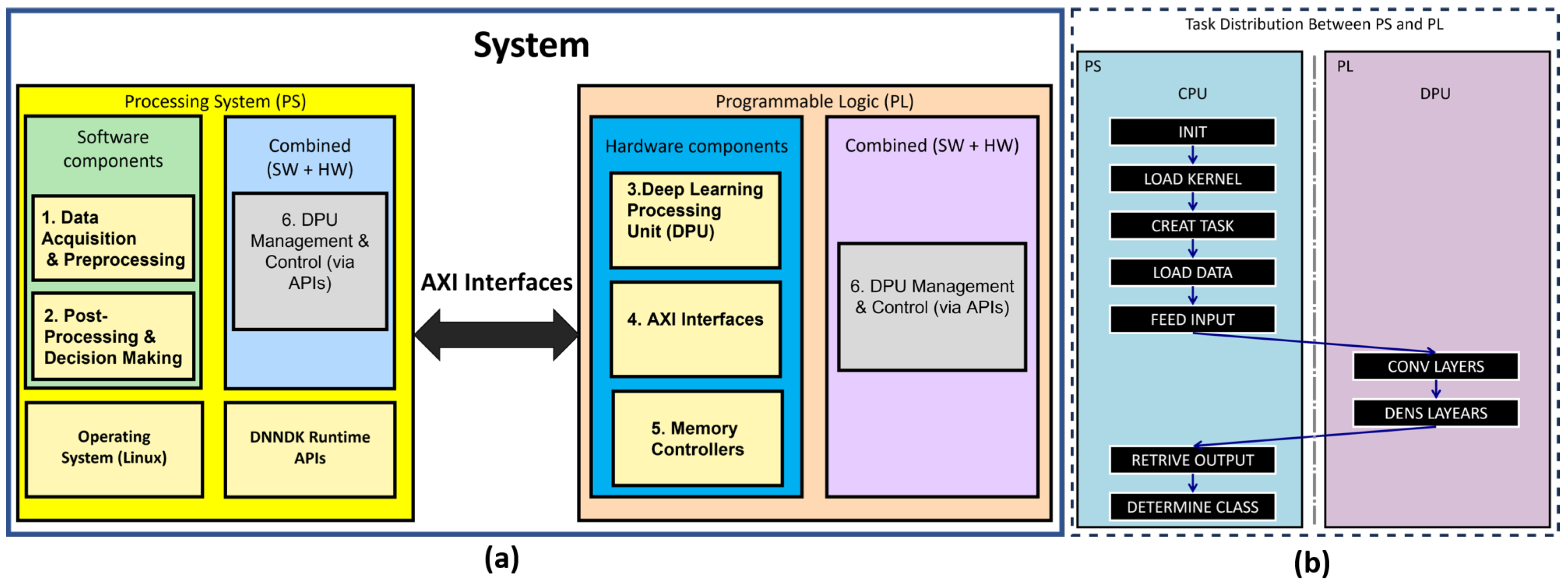
As illustrated in Figure 8, the proposed system architecture demonstrates the interaction between the Processing System (PS) and the Programmable Logic (PL), forming a tightly integrated hardware–software co-processing platform. In the PS, block 1 is responsible for data acquisition and preprocessing, while block 2 handles post-processing and decision-making. The operating system (Linux) provides the execution environment for these tasks. These high-level functions are supported by DNNDK runtime APIs.
Block 6 spans both PS and PL domains and represents the combined management and control mechanism for the DPU. In the PS, this includes software APIs used to configure and trigger inference operations. In the PL, it refers to the hardware modules responsible for receiving commands and handling task execution.
The PL hosts the DPU (block 3), which is responsible for executing compute-intensive layers of the CNN model, such as convolutions and fully connected (dense) layers. Block 4 represents the AXI interfaces that ensure high-throughput communication between the PS and PL. These interfaces facilitate the transfer of input tensors, weights, and output results. Block 5 includes memory controllers that manage access to shared DDR memory, enabling the DPU to autonomously read and write data during inference.
Figure 8b presents the runtime execution flow. The CPU begins by initializing the environment and loading the compiled kernel into the DPU (INIT, LOAD_KERNEL). It then creates the inference task (CREATE_TASK), loads input data (LOAD_DATA), and sends the data to the DPU (FEED_INPUT). The DPU executes the supported layers, including convolution and dense operations, and upon completion, the CPU retrieves the output (RETRIEVE_OUTPUT) and performs the final classification (DETERMINE_CLASS). This tightly coupled flow ensures efficient task partitioning and optimized execution between the software and hardware domains.

3.3.5. HW/SW Co-Design Outcome

The HW/SW co-design phase culminated in the successful integration of the TSRACE-AI system, enabling real-time traffic sign recognition with high performance and energy efficiency. The use of 8-bit quantization, combined with FPGA-based acceleration, reduced model complexity while preserving accuracy. This allowed the system to meet the computational and latency constraints of ADAS applications while minimizing power consumption. Overall, the design confirms the feasibility of deploying lightweight CNN models on resource-constrained edge platforms through a carefully crafted co-design strategy.

4. Experiment and Results

This section evaluates the performance of the TSRACE-AI model deployed on the PYNQ-Z2 platform with the DPU for hardware acceleration. The analysis focuses on latency, throughput, power efficiency, and a comparative assessment with CPU, GPU, and state-of-the-art FPGA-based solutions.

4.1. Resource Utilization

The resource utilization of the FPGA hardware for CNN acceleration is a critical metric that demonstrates the efficiency of the hardware design in making full use of available resources while achieving high performance. The Xilinx Vivado tool provided detailed resource utilization metrics for the implemented design, as summarized in Table 3.
The results highlight that the design utilized 96.36% of the DSP slices, which was expected due to the computationally intensive nature of the convolutional layers. The LUT and BRAM utilization, though lower, remained significant, demonstrating an efficient balance between logic resources and memory elements.

4.2. Latency Analysis

Latency is a critical factor in evaluating the real-time performance of an inference system, especially for autonomous applications. It includes the time required for input preparation, model inference, and output retrieval.
  • Input Latency: As shown in Figure 9, the FPGA demonstrates consistently low input latency, averaging around 0.3 ms across all processed images. This stability is crucial for real-time systems, allowing for predictable response times. In contrast, the CPU and GPU exhibit higher and more variable latencies due to their general-purpose architectures and data handling pipelines.
As shown in the graph, the CPU (red curve) maintains a stable but high latency of approximately 15 ms per image, rendering it less suitable for time-sensitive tasks like TSR in ADAS. The GPU (blue curve) initially experiences high latency but quickly stabilizes below 5 ms after processing a few hundred images, benefiting from warm-up and parallel processing.
The FPGA (green curve) consistently delivers sub-millisecond latency, approximately 1.17 ms per inference (based on a throughput of 205.39 GOPS for a 0.24 GOP model). This predictable and low latency makes the FPGA the most reliable option for real-time deployment, especially where decision-making delays must be minimized.

4.3. Throughput and Real-Time Feasibility

Throughput is defined as the number of inferences completed per second and is inversely related to the total latency:
Throughput = 1 Total Latency ( s )
Given a total latency of approximately 1.17 ms (0.00117 s), the estimated throughput of the FPGA platform is:
Throughput ( FPGA ) = 1 0.00117 854 inferences / sec
Using the same method:
Throughput ( CPU ) = 1 0.015 67 inferences / sec Throughput ( GPU ) 2000 2500
To evaluate real-time capability, consider a vehicle traveling at 120 km/h (33.33 m/s). The distance it travels during inference is:
Distance = Speed · Inference Time = 33.33 · 0.00117 0.039 m
This implies that the vehicle moves less than 4 cm during an FPGA inference, confirming the system’s suitability for fast-response applications like TSR in ADAS.

4.4. Power Efficiency

In power-sensitive applications such as embedded automotive systems, energy efficiency is essential. Table 4 compares the three platforms in terms of computational throughput and power consumption.
While the GPU achieves the highest raw throughput, it consumes significantly more power. The FPGA offers a highly favorable trade-off between latency, throughput, and power, making it the ideal choice for edge deployment. The CPU, though more power-efficient than the GPU, lacks the necessary performance for high-speed inference workloads.
The FPGA platform, with its low latency, acceptable throughput, and excellent power efficiency, emerges as the most balanced solution for deploying CNN-based TSR systems in real-time ADAS scenarios.

4.5. Comparative Analysis with Related Work

To provide context for the performance of our model, Table 5 presents a comparative analysis of the proposed model with several state-of-the-art FPGA implementations from recent research.

4.5.1. Device and Resource Utilization

The proposed model runs on the PYNQ-Z2 platform, which offers significantly fewer resources than high-end devices such as the Stratix 10 NX and Alveo U250. Despite this, TSRACE-AI efficiently utilizes its available resources, using 220 DSPs and achieving 66.72% logic utilization. This represents a major improvement over the previous PYNQ-Z2 implementation [10], which only used 23% of its available logic.
Additionally, TSRACE-AI achieves 87.86% BRAM utilization, a significant improvement compared to the 31% BRAM utilization in the prior PYNQ-Z2 work [10]. This efficient resource management allows TSRACE-AI to handle more complex computations while remaining a cost-effective, lightweight alternative for edge AI tasks.
When compared to other ADAS-focused works, Tatar and Bayar’s [21] multi-task learning system on the XCK26 device uses significantly more hardware resources (774 DSPs and 93.75% BRAM utilization) while operating on a larger UltraScale+ platform. TSRACE-AI achieves competitive utilization efficiency on a smaller device, making it more accessible for cost-sensitive deployments. Similarly, Kim et al. [20] employ only 40 DSPs and 25% BRAM utilization on an XC7Z045, prioritizing ultra-low power usage over raw throughput. While their approach is advantageous for power-constrained systems, TSRACE-AI leverages higher DSP and BRAM usage to deliver substantially lower latency and higher throughput. The same overlay also supports plug-in baselines (VGG-16 and ResNet-20) without regenerating hardware, underscoring the framework’s reusability on fixed resources.

4.5.2. Frequency and Network

TSRACE-AI operates with a dual-frequency configuration to optimize performance and efficiency: a 150 MHz clock drives the AXI interconnects and peripheral logic, while a dedicated 300 MHz clock powers the Deep Processing Unit (DPU) for high-speed neural network computations. This setup ensures sufficient bandwidth for data movement while enabling fast and deterministic inference.
Tatar and Bayar [21] also operate at 300 MHz but without dual-frequency optimization, relying on a uniform clock domain. Kim et al. [20] run their 8-bit CNN at 250 MHz, which is slightly lower than TSRACE-AI’s DPU frequency. The dual-clock approach in TSRACE-AI provides a more balanced trade-off between data transfer and computation, reducing bottlenecks in real-time inference pipelines. On the same clocks and precision, the overlay accommodates two additional plug-in networks with 32 × 32 × 3 inputs: VGG-16 ( C VGG 16 = 0.5703 GOPs/inf) and ResNet-20 ( C R 20 = 0.0816 GOPs/inf), which we contrast with TSRACE-AI ( C ours = 0.241952 GOPs/inf).

4.5.3. Throughput and Latency

The overlay sustains 205.39 GOPS on PYNQ-Z2. Under this setting, TSRACE-AI achieves a latency of 1.17 ms and a throughput of 205.39 GOPS, representing a 200.28% improvement over the previous PYNQ-Z2 implementation [10] (68.4 GOPS) and a 98.85% latency reduction (from 102 ms to 1.17 ms).
To provide an apples-to-apples slice on the same board/clock/precision, we include two plug-in baselines: VGG-16 (32 × 32 × 3, C = 0.5703 GOPs/inf), which yields 2.78 ms latency, and ResNet-20 (32 × 32 × 3, C = 0.0816 GOPs/inf), which yields 0.40 ms latency; TSRACE-AI ( C = 0.241952 GOPs/inf) sits in between at 1.17 ms. This ordering (ResNet-20 < TSRACE-AI < VGG-16) follows directly from the compute budgets under identical platform throughput.
When compared with ADAS-oriented designs, TSRACE-AI offers substantial advantages:
  • Tatar and Bayar [21] achieve 25 GOPS throughput with a latency of 39.37 ms. TSRACE-AI is therefore over 33 × faster in latency and 8 × higher in throughput.
  • Kim et al. [20] report 0.96 GOPS throughput with a latency of 25 ms, optimized for low power rather than speed. TSRACE-AI outperforms this by over 21 × in latency and approximately 214 × in throughput.
For completeness, using P = 4.3 W on our board, the energies per inference are 11.95 mJ (VGG-16), 5.03 mJ (TSRACE-AI), and 1.72 mJ (ResNet-20), computed as P × Latency .

4.5.4. Power Efficiency

TSRACE-AI yields 47.77 GOPS/W (205.39 GOPS at 4.3 W). Several prior works report higher GOPS/W but rely on substantially different conditions: either HBM2 memory systems and larger power envelopes (e.g., Alveo-class devices) or per-model dataflow pipelines that sacrifice generality for extreme locality. Under identical platform settings, the two plug-in baselines on our overlay (VGG-16 and ResNet-20 at 32 × 32 × 3) report the same platform efficiency figure by construction while exhibiting the expected latency ordering driven by their respective compute budgets.
When compared to other ADAS-oriented FPGA designs, Kim et al. [20] exhibit very low power efficiency (0.138 GOPS/W) together with low throughput, making their solution better suited for ultra-low-energy submodules rather than latency-critical perception pipelines. Tatar and Bayar [21] do not explicitly report GOPS/W; based on their reported latency and throughput, TSRACE-AI delivers a more favorable performance–latency profile for real-time operation.
In comparison:
  • BNN-PYNQ and H2PIPE show stronger GOPS/W on larger or specialized devices at higher operating frequencies and with greater resource budgets.
  • TSRACE-AI presents a practical trade-off on DDR-based, low-power hardware: it sacrifices a small efficiency margin to achieve a 98.85% reduction in latency and a ∼3× gain in throughput versus [10] while providing a plug-in path to standard baselines (VGG-16, ResNet-20) under identical deployment constraints.
In many embedded AI applications, particularly in automotive systems like ADAS, latency and responsiveness are critical requirements that often outweigh marginal differences in energy efficiency. Nevertheless, improving energy efficiency remains an important goal for broader deployment in power-constrained edge environments. Future enhancements will focus on optimizing the system’s energy profile by enabling low-power modes in the DPU, leveraging DSP blocks for more efficient arithmetic operations, and incorporating model compression techniques such as structured pruning and quantization-aware training. Additional improvements are expected through dynamic voltage and frequency scaling (DVFS) [36] and by porting the system to more advanced platforms such as Zynq UltraScale+ MPSoCs [37], which offer better performance-per-watt characteristics.

4.5.5. Framework Rationale and Unique Value

We acknowledge that several prior designs report higher GOPS/W; however, they target different operating points (HBM2 memory, larger devices, or per-model dataflow pipelines). Our aim is a deployable, plug-in edge framework on DDR-based, low-power hardware. Concretely, TSRACE-AI offers:
  • Plug-in flexibility on a fixed overlay. The same PYNQ-Z2 DPU (INT8, 150/300 MHz) runs multiple networks without regenerating hardware. Swapping among VGG-16, ResNet-20, and TSRACE-AI exposes accuracy/latency trade-offs under identical platform settings.
  • Deterministic, real-time response at ≤5 W. TSRACE-AI delivers 1.17 ms per decision (ResNet-20: 0.40 ms; VGG-16: 2.78 ms) within a 4.3 W budget—meeting strict ADAS latency targets on a low-cost board.
  • Edge-centric memory assumptions. Our design is tuned for DDR bandwidths typical of embedded platforms; it avoids reliance on HBM2 or oversized devices while still achieving 205.39 GOPS sustained throughput.
  • Transparent, comparable reporting. By separating hardware constants (board/overlay/clock/precision) from model complexity C (GOPs/inf) and using the identities Throughput = C × FPS , Latency = 1000 / FPS , and Efficiency = Throughput / P , we provide reproducible, apples-to-apples comparisons across plug-in models on the same platform.
  • Practical time/energy trade-offs. Under identical settings, the energies per inference are 1.72 mJ (ResNet-20), 5.03 mJ (TSRACE-AI), and 11.95 mJ (VGG-16). These figures, together with sub-millisecond response, reflect application-level utility beyond peak GOPS/W.
In short, TSRACE-AI prioritizes real-time latency, plug-in reuse, and low-cost deployability on DDR FPGAs. This fills a complementary niche to HBM2/dataflow-specialized designs: while those maximize efficiency on larger devices, our framework provides a practical, flexible path to consistent, real-time inference on resource- and power-constrained edge hardware.

5. Conclusions

The development of TSRACE-AI marks a significant advancement in edge AI for traffic sign recognition, achieving an optimal balance between performance and resource efficiency on a resource-constrained PYNQ-Z2 platform. The proposed design delivers a 98.85% latency reduction (from 102 ms to 1.17 ms) and a 200.28% throughput increase (from 68.4 to 205.39 GOPS) compared to the previous state-of-the-art on the same device [10] while maintaining competitive resource utilization and real-time capabilities crucial for Advanced Driver Assistance Systems (ADASs).
Despite operating on a low-cost FPGA, TSRACE-AI achieves sub-millisecond inference latency, outperforming several larger and more power-hungry platforms such as the Stratix 10 NX and Alveo U250 in latency-sensitive applications. This demonstrates the potential of carefully co-designed hardware–software architectures and 8-bit fixed-point quantization to maximize the capabilities of modest hardware.
While the system prioritizes real-time responsiveness over power efficiency (4.96 GOPS/W), it still presents a practical trade-off for safety-critical automotive scenarios where low latency is paramount. Nevertheless, improving energy efficiency remains an important objective. Future work will focus on enabling low-power modes in the DPU, leveraging DSP blocks for more efficient arithmetic, and adopting model compression techniques such as structured pruning and quantization-aware training. Further gains are expected through dynamic voltage and frequency scaling (DVFS) and migration to more advanced FPGA platforms like Zynq UltraScale+ MPSoCs.
Beyond power optimization, a major direction for future research is to enhance detection robustness in complex operational conditions, such as poor illumination, motion blur, occlusion, adverse weather, and visually similar sign patterns. This can be addressed by integrating domain-adaptive training, advanced data augmentation (e.g., synthetic fog/rain/night scenarios), and lightweight attention mechanisms to improve feature discrimination without significantly increasing resource usage.
By combining these improvements in both energy efficiency and detection robustness, TSRACE-AI can evolve into a more versatile and power-aware embedded AI solution, capable of delivering reliable performance in diverse and challenging real-world ADAS deployments.

Author Contributions

A.S. conducted the study, including conceptualization, methodology, data analysis, and manuscript preparation. S.B.A. provided supervision and guidance throughout the research process. A.T. offered technical support. All authors have read and agreed to the published version of the manuscript.

Funding

This research received no external funding.

Institutional Review Board Statement

Not applicable.

Informed Consent Statement

Not applicable.

Data Availability Statement

All materials used in this study are standard and available upon request.

Conflicts of Interest

The authors declare no conflicts of interest.

References

  1. Levinson, J.; Askel, J.; Becker, J.; Dolson, J.; Held, D.; Kammel, S.; Kolter, J.Z.; Langer, D.; Pink, O.; Pratt, V.; et al. Towards fully autonomous driving: Systems and algorithms. In Proceedings of the 2011 IEEE Intelligent Vehicles Symposium (IV), Baden-Baden, Germany, 5–9 June 2011; pp. 163–168. [Google Scholar]
  2. Garikapati, D.; Shetiya, S.S. Autonomous vehicles: Evolution of artificial intelligence and the current industry landscape. Big Data Cogn. Comput. 2024, 8, 42. [Google Scholar] [CrossRef]
  3. Bhatt, D.; Patel, C.; Talsania, H.; Patel, J.; Vaghela, R.; Pandya, S.; Modi, K.; Ghayvat, H. CNN variants for computer vision: History, architecture, application, challenges and future scope. Electronics 2021, 10, 2470. [Google Scholar] [CrossRef]
  4. Cho, M.; Kim, Y. FPGA-based convolutional neural network accelerator with resource-optimized approximate multiply-accumulate unit. Electronics 2021, 10, 2859. [Google Scholar] [CrossRef]
  5. Abbas, N.; Zhang, Y.; Taherkordi, A.; Skeie, T. Mobile edge computing: A survey. IEEE Internet Things J. 2017, 5, 450–465. [Google Scholar] [CrossRef]
  6. Possa, P.; Schaillie, D.; Valderrama, C. FPGA-based hardware acceleration: A CPU/accelerator interface exploration. In Proceedings of the 2011 18th IEEE International Conference on Electronics, Circuits, and Systems, Beirut, Lebanon, 11–14 December 2011; pp. 374–377. [Google Scholar] [CrossRef]
  7. García, G.J.; Jara, C.A.; Pomares, J.; Alabdo, A.; Poggi, L.M.; Torres, F. A survey on FPGA-based sensor systems: Towards intelligent and reconfigurable low-power sensors for computer vision, control and signal processing. Sensors 2014, 14, 6247–6278. [Google Scholar] [CrossRef]
  8. Ghaffar, M.A.; Li, Z.; Chen, T.; Haider, S.A.; Pokharel, M.; Hanifi, S.; Subedi, N. A traffic sign recognition algorithm for ADAS based on CNN for complex scenarios. In Proceedings of the 2023 7th International Conference on Transportation Information and Safety (ICTIS), Xi’an, China, 4–6 August 2023; pp. 1760–1766. [Google Scholar] [CrossRef]
  9. Triki, N.; Karray, M.; Ksantini, M. A real-time traffic sign recognition method using a new attention-based deep convolutional neural network for smart vehicles. Appl. Sci. 2023, 13, 4793. [Google Scholar] [CrossRef]
  10. Gundrapally, A.; Shah, Y.A.; Alnatsheh, N.; Choi, K.K. A high-performance and ultra-low-power accelerator design for advanced deep learning algorithms on an FPGA. Electronics 2024, 13, 2676. [Google Scholar] [CrossRef]
  11. He, K.; Zhang, X.; Ren, S.; Sun, J. Deep residual learning for image recognition. In Proceedings of the IEEE Conference on Computer Vision and Pattern Recognition, Las Vegas, NV, USA, 27–30 June 2016; pp. 770–778. [Google Scholar]
  12. Krizhevsky, A.; Nair, V.; Hinton, G. CIFAR-10 (Canadian Institute for Advanced Research). 2010. Available online: https://academictorrents.com/details/463ba7ec7f37ed414c12fbb71ebf6431eada2d7a (accessed on 15 August 2025).
  13. Doumet, M.; Stan, M.; Hall, M.; Betz, V. H2PIPE: High Throughput CNN Inference on FPGAs with High-Bandwidth Memory. In Proceedings of the 2024 34th International Conference on Field-Programmable Logic and Applications (FPL), Torino, Italy, 2–6 September 2024; pp. 69–77. [Google Scholar]
  14. Gao, X.; Wu, B.; Li, P.; Jing, Z. 1D-CNN-Transformer for Radar Emitter Identification and Implemented on FPGA. Remote Sens. 2024, 16, 2962. [Google Scholar] [CrossRef]
  15. Ajili, M.T.; Hara-Azumi, Y. Multimodal neural network acceleration on a hybrid CPU-FPGA architecture: A case study. IEEE Access 2022, 10, 9603–9617. [Google Scholar] [CrossRef]
  16. Mansouri, A.; Elzaar, A.; Madani, M.; Bakir, T. Design and Hardware Implementation of CNN-GCN Model for Skeleton-Based Human Action Recognition. Wseas Trans. Comput. Res. 2024, 12, 318–327. [Google Scholar] [CrossRef]
  17. Wang, Y.; Liao, Y.; Yang, J.; Wang, H.; Zhao, Y.; Zhang, C.; Xiao, B.; Xu, F.; Gao, Y.; Xu, M. An FPGA-based online reconfigurable CNN edge computing device for object detection. Microelectron. J. 2023, 137, 105805. [Google Scholar] [CrossRef]
  18. Yao, Y.; Duan, Q.; Zhang, Z.; Gao, J.; Wang, J.; Yang, M.; Tao, X.; Lai, J. An FPGA-based hardware accelerator for multiple convolutional neural networks. In Proceedings of the 2018 14th IEEE International Conference on Solid-State and Integrated Circuit Technology (ICSICT), Qingdao, China, 31 October–3 November 2018; pp. 1–3. [Google Scholar] [CrossRef]
  19. Gschwend, D. Zynqnet: An FPGA-accelerated embedded convolutional neural network. arXiv 2020, arXiv:2005.06892. [Google Scholar]
  20. Kim, J.; Kang, J.-K.; Kim, Y. A low-cost fully integer-based CNN accelerator on FPGA for real-time traffic sign recognition. IEEE Access 2022, 10, 84626–84634. [Google Scholar] [CrossRef]
  21. Tatar, G.; Bayar, S. Real-time multi-task ADAS implementation on reconfigurable heterogeneous MPSoC architecture. IEEE Access 2023, 11, 80741–80760. [Google Scholar] [CrossRef]
  22. ResNet-50 PYNQ GitHub. Available online: https://github.com/Xilinx/ResNet50-PYNQ/blob/master/host/README.md (accessed on 6 July 2025).
  23. Nguyen, V.C.; Nakashima, Y. Implementation of fully-pipelined CNN inference accelerator on FPGA and HBM2 platform. IEICE Trans. Inf. Syst. 2023, 106, 1117–1129. [Google Scholar] [CrossRef]
  24. Han, Y.; Oruklu, E. Real-time traffic sign recognition based on Zynq FPGA and ARM SoCs. In Proceedings of the IEEE International Conference on Electro/Information Technology, Milwaukee, WI, USA, 5–7 June 2014; pp. 373–376. [Google Scholar]
  25. DNNDK User Guide (UG1327) v1.6. Available online: https://docs.amd.com/v/u/en-US/ug1327-dnndk-user-guide (accessed on 14 October 2024).
  26. Maillard, P.; Chen, Y.P.; Vidmar, J.; Fraser, N.; Gambardella, G.; Sawant, M.; Voogel, M.L. Radiation-tolerant deep learning processor unit (DPU)-based platform using Xilinx 20-nm Kintex UltraScale FPGA. IEEE Trans. Nucl. Sci. 2022, 70, 714–721. [Google Scholar] [CrossRef]
  27. Abdi, L.; Meddeb, A. Deep learning traffic sign detection, recognition and augmentation. In Proceedings of the Symposium on Applied Computing, Marrakech, Morocco, 4–6 April 2017; pp. 131–136. [Google Scholar]
  28. Gonzalez, R.C.; Woods, R.E. Digital Image Processing, 4th ed.; Pearson Education Limited: New York, NY, USA, 2018. [Google Scholar]
  29. Nwankpa, C.E. Advances in optimisation algorithms and techniques for deep learning. Adv. Sci. Technol. Eng. Syst. J. 2020, 5, 563–577. [Google Scholar] [CrossRef]
  30. Simonyan, K.; Zisserman, A. Very deep convolutional networks for large-scale image recognition. arXiv 2014, arXiv:1409.1556. [Google Scholar] [CrossRef]
  31. Howard, A.G. Mobilenets: Efficient convolutional neural networks for mobile vision applications. arXiv 2017, arXiv:1704.04861. [Google Scholar] [CrossRef]
  32. DPUCZDX8G for Zynq UltraScale+ MPSoCs Product Guide (PG338). Available online: https://docs.amd.com/r/en-US/pg338-dpu/Introduction?tocId=3xsG16y_QFTWvAJKHbisEw (accessed on 7 August 2025).
  33. Venieris, S.I.; Fernandez-Marques, J.; Lane, N.D. Mitigating memory wall effects in CNN engines with on-the-fly weights generation. Acm Trans. Des. Autom. Electron. Syst. 2023, 28, 1–31. [Google Scholar] [CrossRef]
  34. Dong, Q.; Xie, X.; Wang, Z. SWAT: An efficient Swin Transformer accelerator based on FPGA. In Proceedings of the Asia and South Pacific Design Automation Conference (ASP-DAC), Incheon, Republic of Korea, 22–25 January 2024; pp. 515–520. [Google Scholar] [CrossRef]
  35. Huang, M.; Luo, J.; Ding, C.; Wei, Z.; Huang, S.; Yu, H. An integer-only and group-vector systolic accelerator for efficiently mapping vision transformer on edge. IEEE Trans. Circuits Syst. I Regul. Pap. 2023, 70, 5289–5301. [Google Scholar] [CrossRef]
  36. Salameh, A.A.; Baharum, F. Adaptive VLSI design using dynamic voltage and frequency scaling (DVFS) for low-latency IoT communication networks. J. Vlsi Circuits Syst. 2025, 7, 19–25. [Google Scholar]
  37. AMD. Zynq UltraScale+ MPSoC Data Sheet: Overview (DS891) (Rev. 1.11.1, March 18, 2025); AMD Inc.: Santa Clara, CA, USA, 2025; Available online: https://docs.amd.com/v/u/en-US/ds891-zynq-ultrascale-plus-overview (accessed on 10 August 2025).
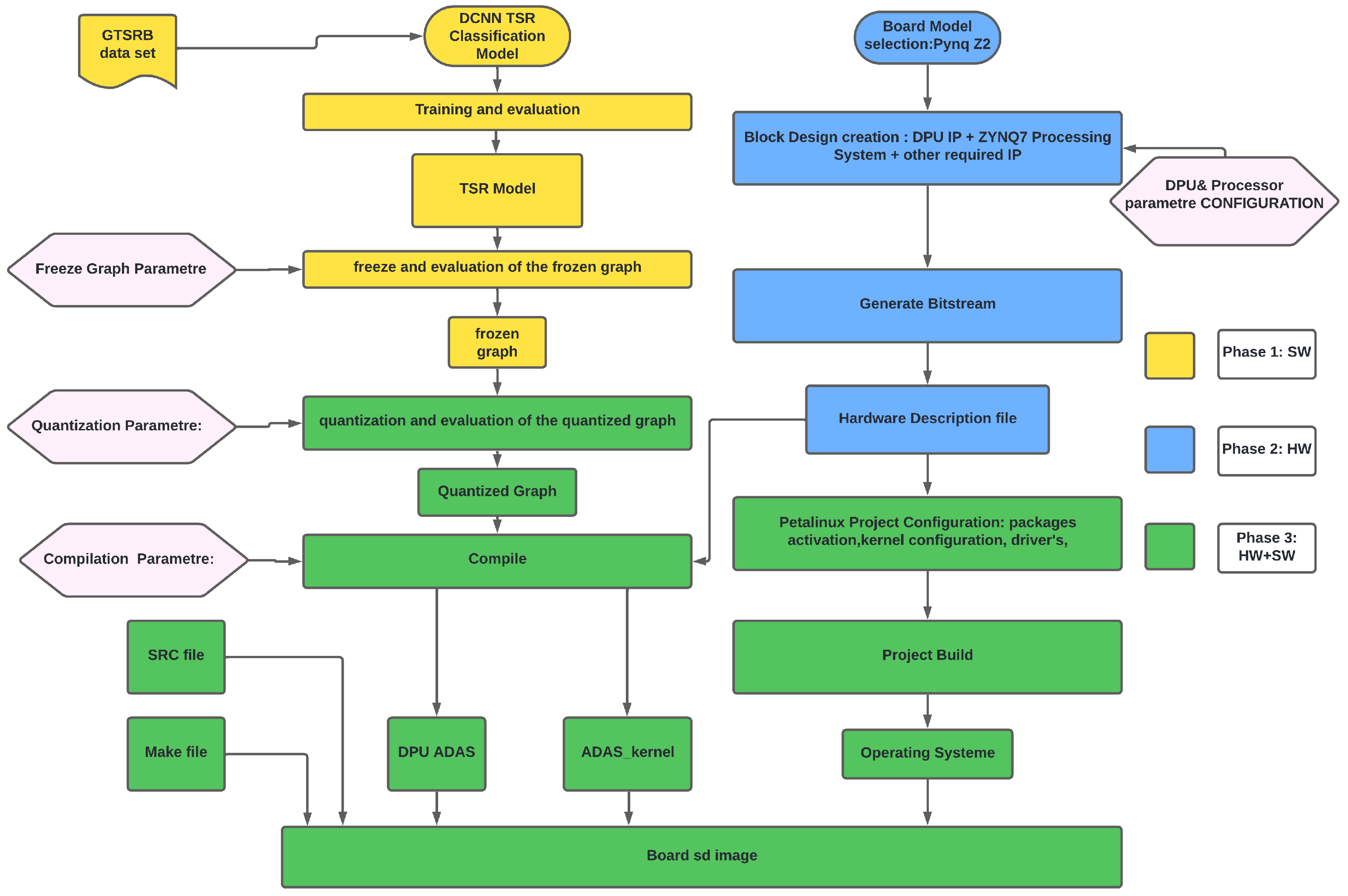
Figure 1. Workflow for the implementation of a DCNN-based Traffic Sign Recognition (TSR) classification model on the PYNQ-Z2 FPGA board. The figure illustrates the three key phases of the design process: software (SW), hardware (HW), and hardware–software (HW-SW) co-design.
Information 16 00703 g001
Figure 2. (a) Model accuracy over 30 epochs for both the training and validation datasets; (b) Model loss over 30 epochs for both the training and validation datasets.
Information 16 00703 g002
Figure 3. Confusion matrix for traffic sign recognition model.
Information 16 00703 g003
Figure 4. Examples of Misclassifications in the Traffic Sign Recognition Model.
Information 16 00703 g004
Figure 5. Deep Learning Processing Unit (DPU) architecture.
Information 16 00703 g005
Figure 6. Block design of DPU integration on Zynq platform.
Information 16 00703 g006
Figure 7. DNNDK-based HW/SW design flow: from FP32 training to INT8 quantization, compilation for DPU v3.0 (B1152), packaging, and deployment on PYNQ-Z2.
Information 16 00703 g007
Figure 8. (a) System architecture with task blocks 1–6; (b) Runtime task distribution between PS and PL.
Information 16 00703 g008
Figure 9. Comparison of latency between CPU, GPU, and FPGA across increasing numbers of processed images.
Information 16 00703 g009
Table 1. Layer-wise computational complexity and parameter summary of the DCNN model.
LayerInput ShapeOutput ShapeNumber of ParametersOperations (M)GOPs
Input Layer(None, 32, 32, 3)(None, 32, 32, 3)000
Conv2D (Layer 1)(None, 32, 32, 3)(None, 28, 28, 32)243256.630.0566
Conv2D (Layer 2)(None, 28, 28, 32)(None, 24, 24, 32)25,632113.660.1137
MaxPooling2D(None, 24, 24, 32)(None, 12, 12, 32)000
Dropout(None, 12, 12, 32)(None, 12, 12, 32)000
Conv2D (Layer 3)(None, 12, 12, 32)(None, 10, 10, 64)18,49633.120.0331
Conv2D (Layer 4)(None, 10, 10, 64)(None, 8, 8, 64)36,92837.990.0380
MaxPooling2D(None, 8, 8, 64)(None, 4, 4, 64)000
Dropout(None, 4, 4, 64)(None, 4, 4, 64)000
Flatten(None, 4, 4, 64)(None, 1024)00.530.0005
Dense (Layer 5)(None, 1024)(None, 256)262,4000.530.0005
Dropout(None, 256)(None, 256)000
Dense (Output)(None, 256)(None, 43)11,0510.0220.00002
Total 356,939242.480.2425
Table 2. DPU configuration for 8-bit quantized CNN on PYNQ-Z2.
ParameterSettings
Number of DPUs1
ArchitectureB1152
RAM UsageLow
DSP UsageLow DSP Mode
Low Power ModeOff
Extra OperationsElementwiseAdd, LeakyReLU
Table 3. Resource utilization summary of FPGA hardware for CNN acceleration.
ResourceUtilizationAvailableUtilization %
LUT35,49553,20066.72%
LUT RAM174417,40010.02%
FF63,779106,40059.94%
BRAM12314087.86%
DSP21222096.36%
BUFG43212.5%
MMCM1425%
Table 4. Performance comparison between FPGA, GPU, and CPU platforms.
PlatformCNN Size (GOP)Throughput (GOPS)Power (W)Power Efficiency (GOPS/W)
FPGA (PYNQ-Z2)0.24205.394.347.76
GPU (RTX 4060 Ti)0.24250014.3174.83
CPU (i7-14700K)0.24679.86.83
Table 5. Comparative analysis of TSRACE-AI with state-of-the-art FPGA implementations.
Reference[33][13][33][22][23][10][34][35][14][21][20]TSRACE-AITSRACE-AI (VGG-16)TSRACE-AI (ResNet-20)
DeviceZ7045Stratix 10 NXZU7EVAlveo U250Alveo U280PYNQ-Z2ALVEO U50ZCU102Xcku040XCK26XC7Z045PYNQ-Z2PYNQ-Z2PYNQ-Z2
Device BRAM (Mb)19.21403843235716.247.332.1-135-16.216.216.2
DSPs9003960172811,508902422059522520-77440220220220
Logic Utilization (%)-678177552331.152.757.354.17-66.7266.7266.72
BRAM Utilization (%)-989197923145.3-64.3393.752587.8687.8687.86
Used DSPs (%)100513314963031.350.351.762.02-96.3696.3696.36
Frequency (MHz)15030020019525050200300150300250150/300150/300150/300
NetworkResNet-18ResNet-18ResNet-50ResNet-50VGG-16ResNet-20Swin-TVIT-Slw-ct PARTYolo ADASCustom CNNCustom CNNVGG-16 (32×32)ResNet-20 (32×32)
Precision16-bit8-bit16-bit1-bit16-bit16-bitint16/int8int8int16QAT-INT8INT88-bit8-bit8-bit
Throughput (GOPS)59.741741004527912.768.4301.9153.2153.2250.96205.39205.39205.39
Latency (ms)16.751.019.481.90.704102-0.37520.375239.37251.172.780.40
GOPs23615,109773135670.6436.97---25-0.2419520.57030.0816
Power (W)----40.61.33114.3529.65.727.196.954.34.34.3
Power Efficiency (GOPS/W)---51.3822.4851.3821.0425.7626.783.470.13847.7747.7747.77
Disclaimer/Publisher’s Note: The statements, opinions and data contained in all publications are solely those of the individual author(s) and contributor(s) and not of MDPI and/or the editor(s). MDPI and/or the editor(s) disclaim responsibility for any injury to people or property resulting from any ideas, methods, instructions or products referred to in the content.