Article

A Methodology to Distribute On-Chip Voltage Regulators to Improve the Security of Hardware Masking

by
Soner Seçkiner
* and
Selçuk Köse
Department of Electrical and Computer Engineering, University of Rochester, Rochester, NY 14627, USA
*
Author to whom correspondence should be addressed.
Information 2024, 15(8), 488; https://doi.org/10.3390/info15080488
Submission received: 12 June 2024 / Revised: 20 July 2024 / Accepted: 13 August 2024 / Published: 16 August 2024
(This article belongs to the Special Issue Hardware Security and Trust)

Abstract

:
Hardware masking is used to protect against side-channel attacks by splitting sensitive information into different parts, called hardware masking shares. Ideally, a side-channel attack would only work if all these parts were completely independent. But in real-world VLSI implementations, things are not perfect. Information from a hardware masking share can leak to another, making it possible for side-channel attacks to succeed without needing data from every hardware masking share. The theoretically supposed independence of these shares often does not hold up in practice. The effectiveness of hardware masking is reduced because of the parasitic impedance that stems from power delivery networks or the internal structure of the integrated circuit. When the coupling effect and noise spread among the hardware masking shares powered by the same power delivery network, side-channel attacks can be carried out with fewer measurements. To address this, we propose a new method of distributing on-chip voltage regulators to improve hardware masking security. The benefits of distributed on-chip voltage regulators are evident. Placing the regulators close to the load minimizes power loss due to resistive losses in the power delivery network. Localized regulation allows for more efficient adjustments to the varying power demands of different chip sections, improving overall power efficiency. Additionally, distributed regulators can quickly respond to power demand changes, maintaining stable voltage levels for high-performance circuits, leading to improved control over noise. We introduce a new DLDO voltage regulator that uses random clocking and randomizing limit cycle oscillations to enhance security. Our simulations show that with these distributed DLDO regulators, the t-test value can be as low as 2.019, and typically, a circuit with a t-test value below 4.5 is considered secure.

1. Introduction

The privacy and security of modern computing devices have become crucial, as these devices are increasingly integrated into our daily lives. Cryptographic algorithms are therefore implemented to secure and protect the privacy of data. Lightweight encryption and decryption are used to achieve fast and power-efficient performance, but side-channel attacks still pose a threat to the security of these cryptographic devices. Attackers can obtain critically sensitive values of an encryption algorithm to reveal sensitive information via physical leakage signatures. To prevent private data leakage, various countermeasures have been developed [1,2]. These countermeasures against side-channel attacks can generally be classified into two main strategies: (i) shuffling and (ii) hiding the private data. Masking-based countermeasures fall under the shuffling category, where an n-bit secret is divided into N shares, akin to multi-party computation.
The hiding countermeasures require strict conditions such as aligned signal propagation and balanced routing to achieve acceptable protection. However, meeting these strict conditions is challenging due to the parasitic effects of advanced technology nodes in various conditions [3]. A well-performing preprocessing and machine learning approach has the potential to extract information from an encryption device that incorporates inadequate security measures. Among the array of countermeasures available, hardware masking is commonly effective in thwarting different attack methods, thanks to its resilient design supported by theoretical foundations [4].
Masking involves partitioning the critically sensitive information into a set of d + 1 shares, a configuration commonly used in dth-order Boolean masking. In this arrangement, the sensitive information is the combined result of Boolean addition applied to each of these shares. The computations within each share are not concealed, and standard dth-order hardware masking can be overcome by a more advanced ( d + 1 ) th-order side-channel attack. The success of effective masking rests on the fundamental assumption that the shares constituting a masking operation are independent. This assumption’s significance cannot be underestimated, as any deviation from independence can result in information leakage due to correlation among the shares. Such leaks can lead to a dth-order attack becoming successful against an encryption device protected by dth-order hardware masking. While dth-order hardware masking enhances security by splitting sensitive data into multiple hardware masking shares, any compromise in the independence of these shares can expose the system to serious security vulnerabilities [5]. Hardware masking can be implemented either in software or hardware. The software-based approach to hardware masking tends to be inherently sequential and can incur substantial costs due to lengthy execution times and extensive code size [6]. In contrast, hardware-based masking capitalizes on its inherent parallelism, making it exceptionally adaptable. This characteristic suits it well for applications demanding high-performance capabilities.
Challenges in implementing hardware masking practically arise from issues like parasitic impedances, transistor variations, and interconnection modifications caused by aging, temperature shifts, and manufacturing processes, making it difficult to maintain the assumption of independent masking shares. The distance between theory and hardware masking practice arises from the persistent Hamming distance leakage due to shared integrated circuit components among hardware masking shares; interdependent leakage caused by chip manufacturing techniques; and the propagation of glitches through logic gates and between hardware masking shares. The literature extensively explores the interdependence of hardware masking shares and applicable mitigation strategies [4,5,7,8,9,10,11,12,13].
Despite numerous countermeasures against side-channel attacks, few specifically address the vulnerabilities associated with hardware masking. While voltage fluctuations in the power delivery network (PDN) have been well explored, the security implications of noise on hardware masking are often overlooked [14,15]. Many studies [16,17,18] focus on using voltage regulators to conceal power signatures from potential adversaries. In contrast, our work emphasizes enhancing the security of hardware masking by dividing sensitive information into masking shares. We specifically utilize a proposed Digital Low Dropout Regulator (DLDO) to improve security, whereas previous works [17,18] have employed buck, LDO, and switch capacitor voltage regulators to obscure leakage signatures. To our knowledge, only a few studies [19,20,21] have examined the security vulnerabilities of hardware masking within the application-specific integrated circuit (ASIC) design flow, without considering on-chip voltage regulators. Thus, we propose a lightweight integration of countermeasures to enhance hardware masking security through voltage regulators. This approach can be applied to any hardware masking implementation across various encryption algorithms.
The advantages of distributed on-chip voltage regulators can be listed in the aforementioned advantages. By positioning the voltage regulators near the load, the power loss from resistive losses in the power delivery network is minimized. Localized regulation can more efficiently adjust to the varying power demands of different chip sections, enhancing overall power efficiency. Distributed regulators can quickly respond to changes in power demand, maintaining control of the voltage levels for high-performance circuits. We leverage the benefits of distributed on-chip voltage regulators and carefully manage the noise they generate.
Firstly, to our knowledge, this is the first time that a proposed Digital Low Dropout Regulator (DLDO) has been utilized to enhance the security of hardware masking by introducing random delays and amplitudes of limit cycle oscillation. Secondly, we validate the methodology to distribute on-chip voltage regulators into quadrants on the power delivery network, demonstrating that the security of hardware masking improves as the on-chip voltage regulators are placed at a close distance to the hardware masking shares. Thirdly, we propose a security evaluation with test vector leakage assessment (TVLA) for each quadrant of the power delivery network to assess the impact of various voltage regulator topologies and placement strategies.
In addition to the previous contributions, the pre-silicon evaluation framework is proposed since the evaluation framework in pre-silicon is not common [22]. The vulnerabilities due to the effects are determined and eliminated in this framework. On the other hand, during the post-silicon phase, accessing comprehensive design details might not be feasible, particularly when employing third-party components. As a result, pinpointing the origin of leakage can pose difficulties. Furthermore, the tasks of identifying, confirming, and addressing side-channel leaks necessitate specialized expertise and costly equipment.

2. Distributed On-Chip Voltage Regulators

An off-chip voltage source, whether from a battery or an external voltage converter, is connected to the on-chip global power grid through a pad on the integrated circuit. Modern systems typically incorporate both off-chip and on-chip voltage converters. The global power grid’s voltage is then regulated and adjusted to various levels for different load circuits via a local power grid. This power grid consists of orthogonal metal lines linked by vias. Because of the complex routing between loads and voltage regulators, the resistive effects of the power grid become significant. This results in an IR drop, causing voltage drops within the same power distribution grid to be correlated. On-chip voltage regulators are strategically placed to manage this correlation and keep it within acceptable bounds. The approach outlined in the preceding sections is designed to reduce the correlation between load circuits, thereby enhancing the security of on-chip circuits, particularly those used for cryptographic functions.
A simplified power delivery network (PDN) can be observed in Figure 1. An external power source is the main power source of the integrated circuit where the parasitic resistances due to the external effects are lumped in R E x t e r n a l . The voltage is regulated with an on-chip voltage regulator to obtain a stable voltage level for the integrated circuit. The parasitic resistances are represented as R s , R 1 , R 2 , and R 3 . The parasitic capacitances are C 1 , C 2 , and C 3 . The C d e c a p is added to provide better on-chip voltage regulation. The voltages to Share 1 and Share 2, V 1 and V 2 , decrease from the desired voltage levels due to the parasitic effects on the power delivery network. The internal parasitic elements are due to the internal metal layers, internal structures of transistors, and capacitances between internal layers. The external parasitic effects are due to the external metal layers, which carry power from the external power source and integrated circuit. The effect of inductive parasitics may be added series to the parasitic resistances for further analyses but this simplified power delivery network is sufficient to represent the details.
The aforementioned sections describe a methodology to decrease the correlation between load circuits to improve the security of the on-chip circuits, which are designed to improve the security of the cryptographic circuits.

2.1. Proposed Algorithm

Welch’s t-test [23] is used to determine if a circuit’s behavior differs under two distinct inputs, such as a fixed input versus a random one. The test statistic is given by
t ( X , Y ) = E ( X ) E ( Y ) σ X 2 N X + σ Y 2 N Y ,
where X and Y represent two random distributions, E(X) and E(Y) are their expected values, and σ X and σ Y are the standard deviations of X and Y, respectively. This hypothesis testing method assesses the similarity between X and Y. If the computed t-test value is less than 4.5, the test provides a 99.99% confidence interval, indicating that X is statistically different from Y. Consequently, t-test values below 4.5 are generally considered to show no significant leakage [5,7,19].
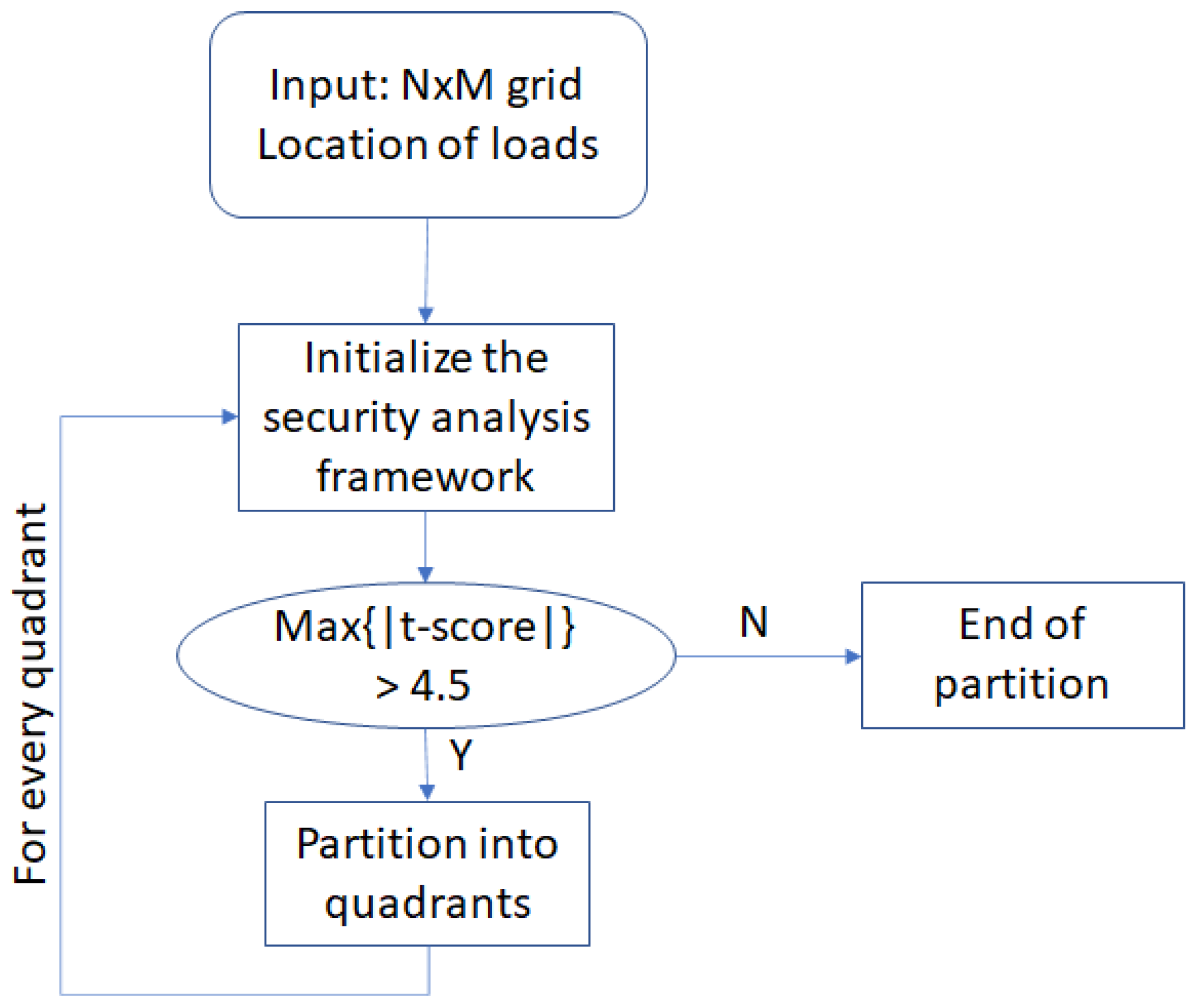
The iterative process of partitioning the PDN into quadrants is shown in Figure 2. Each quadrant has a dedicated on-chip voltage regulator in the center of the quadrant. The voltage fluctuations are minimized to obtain the m a x | t s c o r e | under 4.5. To describe the iterative progress in Figure 2, the power grid is divided into four quadrants at the first round of iteration as can be observed in Figure 3.

2.2. Proposed Digital Low Dropout Voltage Regulators

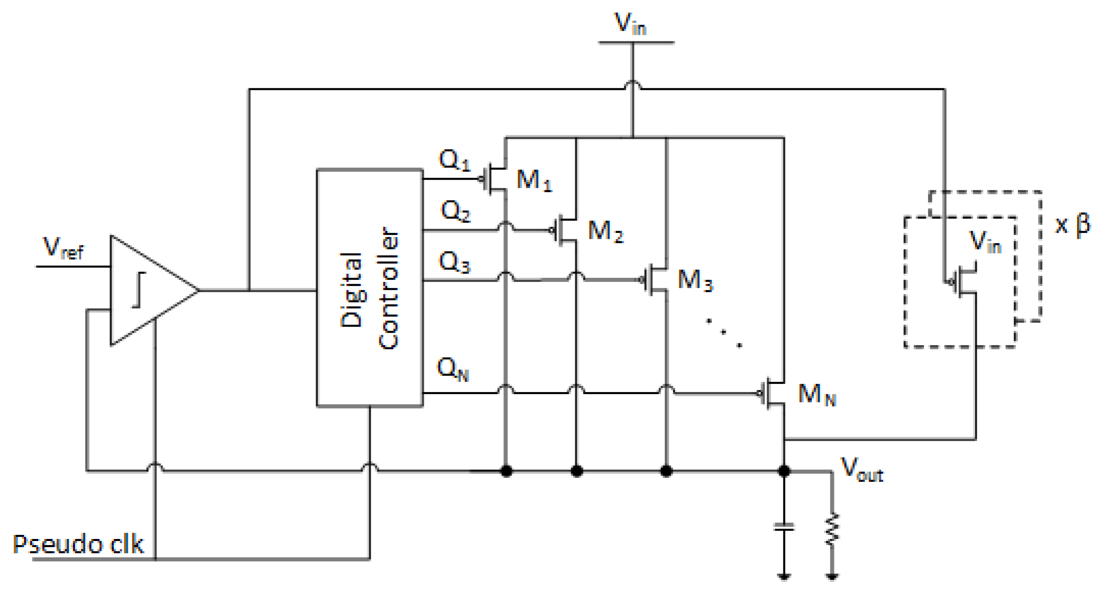
The schematic of the proposed Digital Low Dropout Regulator (DLDO) is shown in Figure 4. In this design, V r e f and P s e u d o   c l k serve as the inputs, while V o u t is the output. Figure 5 and Figure 6 detail the schematic and operational principles of the bi-directional shift register used in conventional DLDOs. The bi-directional shift register in this context includes a multiplexer and a D flip-flop (DFF) in each stage. The digital controller adjusts the value Q i as depicted in Figure 6. The DLDO setup features N parallel PMOS transistors and a feedback control mechanism for output voltage regulation. In conventional DLDOs, a bi-directional shift register is employed. Here, M i denotes the ith PMOS transistor, and Q i represents the output from the digital controller, with ith indicating the activation stage of the digital controller. The shift register toggles the state of one of the power transistors based on V c m p at each rising edge of the p s e u d o   c l k cycle. Q N represents the Nth output signal of the digital controller as illustrated in Figure 4. During step k + 1 , if V c m p is high, Q n + 1 ( Q n ) is activated on (off) with the bi-directional shift register shifting to the right. Conversely, if V c m p is low, the shift register moves to the left as shown in Figure 6 [24]. Each M n is linked to Q n , and due to the bi-directional activation scheme, the transistors M 1 through M n experience high usage. The limit cycle reduction technique from [25] is applied in a randomized behavior. This technique connects four parallel PMOS transistors to V o u t , randomizing limit cycle operations for more efficient, reliable, and secure voltage regulation.
A new DLDO with a p s e u d o   c l k and randomly gated PMOS at limit cycle reduction is proposed. The p s e u d o   c l k signal is generated with different frequencies at the operation of the DLDO, leading to frequency modulation at the digital controller. The frequency of the digital controller changes randomly between 50 Mhz and 2 Ghz in the time domain operation of DLDO. The frequency change in the time domain creates delays in the sampling of the output voltage, leading to different limit cycle values at the output of the DLDO. The random delays create noise in the output of the DLDO without affecting the efficiency. Another randomization stage is added with the limit cycle reduction circuit. Four PMOS transistors are gated randomly during the operation of the DLDO. The β value is changed randomly between one and four at the regular operation of DLDO. This change creates a random limit cycle reduction at the output of the DLDO, leading to noise which can improve the security. The effect of the security improvement is discussed in the analysis section.

2.3. Proposed Pre-Silicon Leakage Detection Framework

The proposed analysis framework consists of two stages: dynamic analyses and security analyses. The layout netlist contains the switching circuits with countermeasures and other circuits. The 32 nm PTM technology is used for the framework. We collect 100 k power traces with constant input and random input to the circuit, where the operation of the circuit is dependent on the variation in the input. We analyze a 16 × 16 resistive PDN with ideal voltage regulators and the proposed DLDO with Finesim. The TVLA method is utilized for the security analyses which contains the calculation of t-score, i.e., fixed vs. random t test. The flowchart of the proposed pre-silicon leakage detection framework is summarized in Figure 7.

3. Power Grid Analyses

The proposed methodology to distribute voltage regulators and the proposed DLDO are analyzed with the hardware masking. The second-order hardware masking circuits are analyzed on a 16 × 16 resistive PDN with the grid resistance 5 Ω .

3.1. Distribution of Ideal Voltage Regulators

The proposed distribution of voltage regulators framework is applied to the second-order hardware masking. One of the hardware masking shares is located at the bottom left, and the other hardware masking share is located on the top right of the PDN as can be observed in Figure 8. The ideal voltage regulator is located at the center of the PDN, and the m a x | t s c o r e | is 8.302, which is higher than the desired security level, i.e., 4.5. Therefore, the PDN is divided into quadrants. All the quadrants except the bottom left quadrant satisfy the security level defined in the t-test. The bottom left quadrant is also divided into quadrants. The seven ideal voltage regulators satisfy the required security level. The m a x | t s c o r e | is reported in Figure 8, where the required security is satisfied in (c). The minimum m a x | t s c o r e | is 2.321, and the maximum m a x | t s c o r e | is 3.258.

3.2. Distribution of Conventional DLDO Voltage Regulators

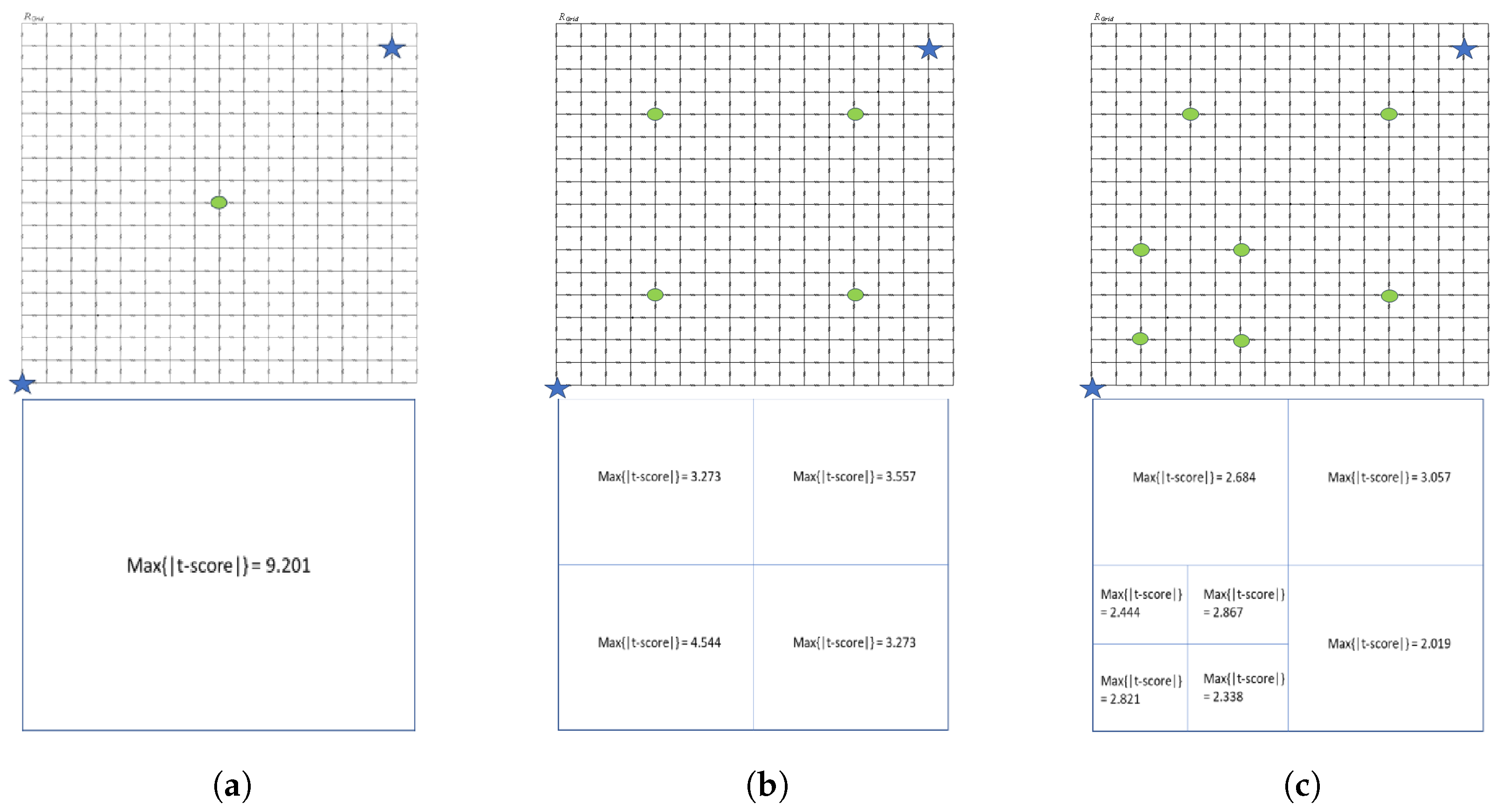
The proposed distribution of voltage regulators framework is applied to the second-order hardware masking with the conventional DLDO. The one hardware masking share is located at the bottom left, and the other hardware masking share is located on the top right of the PDN as can be observed in Figure 9. The m a x | t s c o r e | reduces with four conventional DLDO voltage regulators placed on the center of the quadrants. The seven conventional DLDO voltage regulators satisfy the required security level as compared to the ideal voltage regulators distributed on the PDNp; the required voltage regulator remains the same as the ideal voltage regulator. The use of conventional DLDO has a similar effect to the ideal voltage regulators. The minimum m a x | t s c o r e | reduces to 2.019, which implies that the conventional DLDO has contributed to the security of the hardware masking.

3.3. Distribution of Proposed DLDO Voltage Regulators

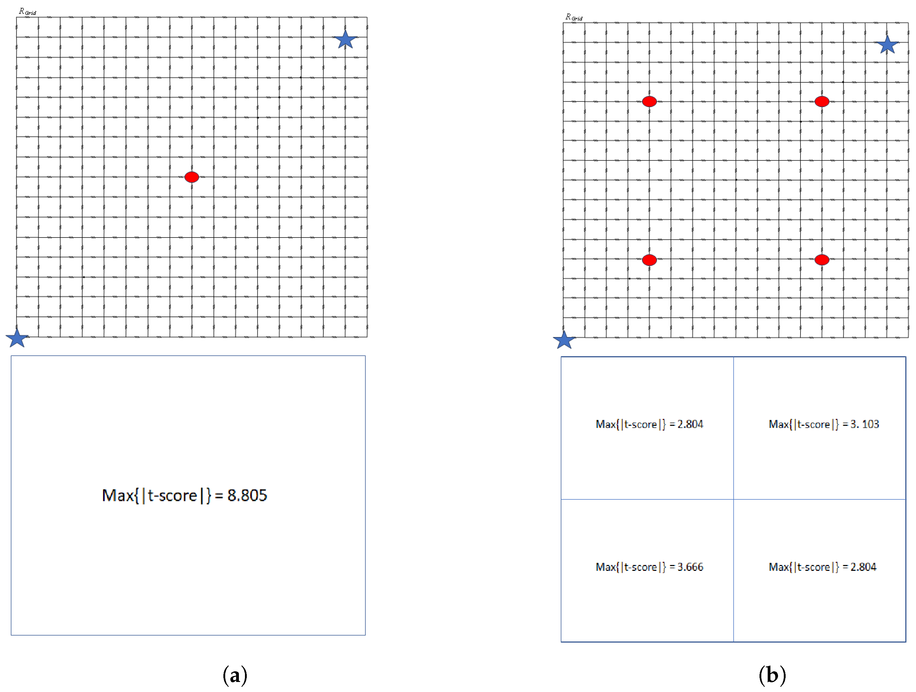
The proposed distribution of voltage regulators framework is applied to the second-order hardware masking with the proposed DLDO. The one hardware masking share is located at the bottom left, and the other hardware masking share is located on the top right of the PDN as can be observed in Figure 10. The m a x | t s c o r e | reduces significantly with four proposed DLDO voltage regulators placed in the center of the quadrants. The four proposed DLDO voltage regulators satisfy the required security level as compared to ideal voltage regulators and conventional DLDO distributed on the PDN; the required voltage regulator reduces from seven to four. The effect of the noise which was generated with the frequency modulation and limit cycle oscillation randomization reduced the number of voltage regulators to satisfy the required security level.
The comparison of the other methods is given in Table 1, where X means that there are no corresponding results published in the work. This work focuses on the utilization of on-chip voltage regulators on the PDN in application-specific integrated circuits (ASICs). The implementation of this work focuses on the PDN on ASIC; thus the focus of comparison of this table is based on the PDN. There are different topologies used in the literature. The common topologies are top–bottom topology and daisy chain topology [27,28,29]. Seven conventional DLDOs are distributed according to the proposed topology, top–bottom, and daisy chain, where the details can be observed in Figure 11. The m a x ( | t s c o r e | ) for top–bottom topology is 5.061, the m a x ( | t s c o r e | ) for daisy chain topology is 3.904, and the m a x ( | t s c o r e | ) for the proposed topology is 2.605 in Table 2, where a m a x ( | t s c o r e | ) below 4.5 is considered to be no significant leakage, and the lower values for the m a x ( | t s c o r e | ) are considered secure. The m a x ( | t s c o r e | ) is the lowest for this work compared to other distribution methodologies.

4. Conclusions

A new methodology to distribute the voltage regulators is proposed to improve the security of the PDN. A new and efficient DLDO is proposed to improve the security of the PDN. The framework is tested on the second-order hardware masking on the 16 × 16 PDN. The seven ideal voltage regulators and conventional DLDO voltage regulators are distributed on the 16 × 16 grid PDN, satisfying the security requirements of the PDN as can be understood by comparing the m a x | t s c o r e | values within the PDN. The proposed framework with the proposed DLDO voltage regulator reduces the required number of voltage regulators by three. The proposed method to distribute the on-chip voltage regulators proved its effectiveness with the ideal voltage regulators, conventional DLDO voltage regulators, and proposed DLDO voltage regulators, with the m a x | t s c o r e | becoming as low as 2.019 with the 16 × 16 grid PDN.

Author Contributions

Writing—original draft, S.S.; Writing—review & editing, S.K. All authors have read and agreed to the published version of the manuscript.

Funding

This research received no external funding.

Institutional Review Board Statement

Not applicable.

Informed Consent Statement

Not applicable.

Data Availability Statement

The original contributions presented in the study are included in the article, further inquiries can be directed to the corresponding author.

Conflicts of Interest

The authors declare no conflicts of interest.

References

  1. Mayhew, M.; Muresan, R. On-chip nanoscale capacitor decoupling architectures for hardware security. IEEE Trans. Emerg. Top. Comput. 2014, 2, 4–15. [Google Scholar] [CrossRef]
  2. Yu, W.; Köse, S. Time-delayed converter-reshuffling: An efficient and secure power delivery architecture. IEEE Embed. Syst. Lett. 2015, 7, 73–76. [Google Scholar] [CrossRef]
  3. Nawaz, K.; Kamel, D.; Standaert, F.X.; Flandre, D. Scaling trends for dual-rail logic styles against side-channel attacks: A case-study. In Proceedings of the International Workshop on Constructive Side-Channel Analysis and Secure Design, Paris, France, 13–14 April 2017; pp. 19–33. [Google Scholar]
  4. Duc, A.; Faust, S.; Standaert, F.X. Making masking security proofs concrete (or how to evaluate the security of any leaking device), extended version. J. Cryptol. 2019, 32, 1263–1297. [Google Scholar] [CrossRef]
  5. De Cnudde, T.; Ender, M.; Moradi, A. Hardware masking, revisited. IACR Trans. Cryptogr. Hardw. Embed. Syst. 2018, 2018, 123–148. [Google Scholar] [CrossRef]
  6. Balasch, J.; Gierlichs, B.; Grosso, V.; Reparaz, O.; Standaert, F.X. On the cost of lazy engineering for masked software implementations. In Proceedings of the International Conference on Smart Card Research and Advanced Applications, Paris, France, 5–7 November 2014; pp. 64–81. [Google Scholar]
  7. Šijačić, D.; Balasch, J.; Verbauwhede, I. Sweeping for leakage in masked circuit layouts. In Proceedings of the Design, Automation and Test in Europe Conference and Exhibition, Grenoble, France, 9–13 March 2020; pp. 915–920. [Google Scholar]
  8. Dai, H.; Köse, S. On the vulnerability of hardware masking in practical implementations. In Proceedings of the 2021 on Great Lakes Symposium on VLSI, Virtual Event, 22–25 June 2021; pp. 77–82. [Google Scholar]
  9. Dyrkolbotn, G.O.; Wold, K.; Snekkenes, E. Security implications of crosstalk in switching cmos gates. In Proceedings of the International Conference on Information Security, Boca Raton, FL, USA, 25–28 October 2010; pp. 269–275. [Google Scholar]
  10. Giechaskiel, I.; Eguro, K. Information leakage between FPGA long wires. arXiv 2016, arXiv:1611.08882. [Google Scholar]
  11. Zussa, L.; Exurville, I.; Dutertre, J.M.; Rigaud, J.B.; Robisson, B.; Tria, A.; Clediere, J. Evidence of an information leakage between logically independent blocks. In Proceedings of the Second Workshop on Cryptography and Security in Computing Systems, Amsterdam, The Netherlands, 19–21 January 2015; pp. 25–30. [Google Scholar]
  12. Schellenberg, F.; Gnad, D.R.; Moradi, A.; Tahoori, M.B. An inside job: Remote power analysis attacks on FPGAs. In Proceedings of the Design, Automation & Test in Europe Conference & Exhibition, Dresden, Germany, 19–23 March 2018; pp. 1111–1116. [Google Scholar]
  13. De Cnudde, T.; Bilgin, B.; Gierlichs, B.; Nikov, V.; Nikova, S.; Rijmen, V. Does coupling affect the security of masked implementations? In Proceedings of the International Workshop on Constructive Side-Channel Analysis and Secure Design, Paris, France, 13–14 April 2017; pp. 1–18. [Google Scholar]
  14. Addisu, M.; Salau, A.O.; Takele, H. Fuzzy logic based optimal placement of voltage regulators and capacitors for distribution systems efficiency improvement. Heliyon 2021, 7, e07848. [Google Scholar] [CrossRef] [PubMed]
  15. Salau, A.; Nweke, J.; Ogbuefi, U. Effective implementation of mitigation measures against voltage collapse in distribution power systems. Prz. Elektrotechniczny 2021, 97, 65–68. [Google Scholar] [CrossRef]
  16. Kar, M.; Singh, A.; Mathew, S.; Rajan, A.; De, V.; Mukhopadhyay, S. Exploiting fully integrated inductive voltage regulators to improve side channel resistance of encryption engines. In Proceedings of the International Symposium on Low Power Electronics and Design, San Francisco, CA, USA, 8–10 August 2016; pp. 130–135. [Google Scholar]
  17. Yu, W.; Köse, S. Exploiting voltage regulators to enhance various power attack countermeasures. IEEE Trans. Emerg. Top. Comput. 2016, 6, 244–257. [Google Scholar] [CrossRef]
  18. Yu, W.; Uzun, O.A.; Köse, S. Leveraging on-chip voltage regulators as a countermeasure against side-channel attacks. In Proceedings of the IEEE/ACM Design Automation Conference, San Francisco, CA, USA, 8–12 June 2015; pp. 1–6. [Google Scholar]
  19. Sijacic, D.; Balasch, J.; Yang, B.; Ghosh, S.; Verbauwhede, I. Towards efficient and automated side channel evaluations at design time. Kalpa Publ. Comput. 2018, 7, 16–31. [Google Scholar]
  20. Monta, K.; Sonoda, H.; Okidono, T.; Araga, Y.; Watanabe, N.; Shimamoto, H.; Kikuchi, K.; Miura, N.; Miki, T.; Nagata, M. 3-D CMOS chip stacking for security ICs featuring backside buried metal power delivery networks with distributed capacitance. IEEE Trans. Electron Devices 2021, 68, 2077–2082. [Google Scholar] [CrossRef]
  21. Dey, S.; Park, J.; Pundir, N.; Saha, D.; Shuvo, A.M.; Mehta, D.; Asadi, N.; Rahman, F.; Farahmandi, F.; Tehranipoor, M. Secure Physical Design. Cryptology ePrint Archive, Paper 2022/891, 2022.
  22. Buhan, I.; Batina, L.; Yarom, Y.; Schaumont, P. SoK: Design tools for side-channel-aware implementations. In Proceedings of the ACM on Asia Conference on Computer and Communications Security, Nagasaki, Japan, 30 May–3 June 2022; pp. 756–770. [Google Scholar]
  23. Gilbert Goodwill, B.J.; Jaffe, J.; Rohatgi, P. A testing methodology for side-channel resistance validation. In Proceedings of the NIST Non-Invasive Attack Testing Workshop, Nara, Japan, 25–27 September 2011; Volume 7, pp. 115–136. [Google Scholar]
  24. Wang, L.; Khatamifard, S.K.; Karpuzcu, U.R.; Köse, S. Mitigation of NBTI induced performance degradation in on-chip digital LDOs. In Proceedings of the Design, Automation & Test in Europe Conference & Exhibition (DATE), Dresden, Germany, 19–23 March 2018; pp. 803–808. [Google Scholar]
  25. Huang, M.; Lu, Y.; Sin, S.W.; Seng-Pan, U.; Martins, R.P.; Ki, W.H. Limit cycle oscillation reduction for digital low dropout regulators. IEEE Trans. Circuits Syst. II Express Briefs 2016, 63, 903–907. [Google Scholar] [CrossRef]
  26. Okuma, Y.; Ishida, K.; Ryu, Y.; Zhang, X.; Chen, P.H.; Watanabe, K.; Takamiya, M.; Sakurai, T. 0.5-V input digital LDO with 98.7% current efficiency and 2.7-μA quiescent current in 65nm CMOS. In Proceedings of the IEEE Custom Integrated Circuits Conference, San Jose, CA, USA, 19–22 September 2010; pp. 1–4. [Google Scholar]
  27. Singh, T.; Schaefer, A.; Rangarajan, S.; John, D.; Henrion, C.; Schreiber, R.; Rodriguez, M.; Kosonocky, S.; Naffziger, S.; Novak, A. Zen: An Energy-Efficient High-Performance x86 Core. IEEE J. Solid-State Circuits 2017, 53, 102–114. [Google Scholar] [CrossRef]
  28. Muthukaruppan, R.; Mahajan, T.; Krishnamurthy, H.K.; Mangal, S.; Dhanashekar, A.; Ghayal, R.; De, V. A digitally controlled linear regulator for per-core wide-range DVFS of atom™ cores in 14nm tri-gate CMOS featuring non-linear control, adaptive gain and code roaming. In Proceedings of the ESSCIRC 2017-43rd IEEE European Solid State Circuits Conference, Leuven, Belgium, 11–14 September 2017; pp. 275–278. [Google Scholar]
  29. Gomes, L.M.G. Power Reduction of a CMOS High-Speed Interface Using Power Gating. 2013.
  30. Seçkiner, S.; Köse, S. Exploiting On-Chip Voltage Regulators for Leakage Reduction in Hardware Masking. Sensors 2022, 22, 7028. [Google Scholar] [CrossRef] [PubMed]
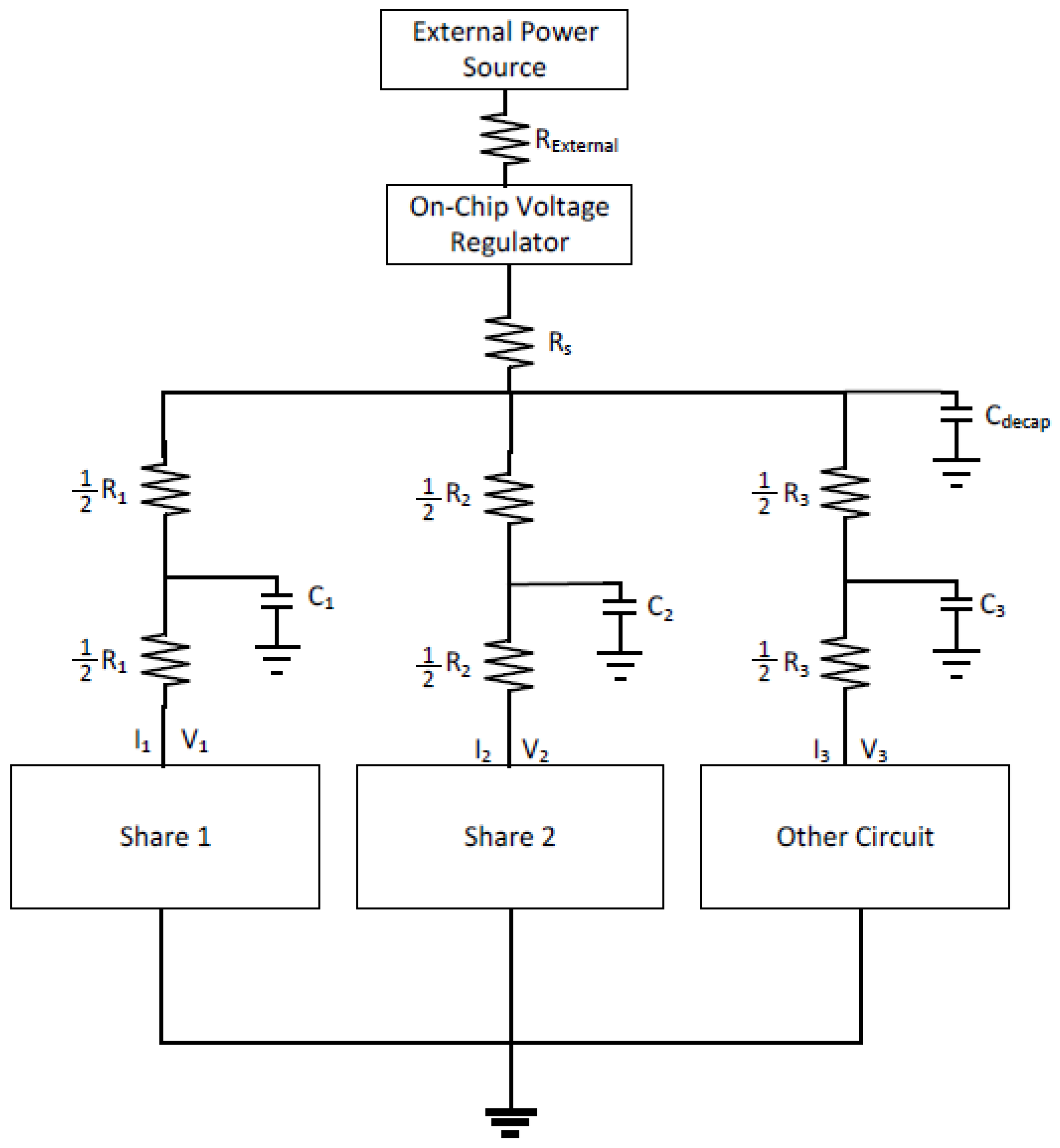
Figure 1. Simplified PDN model with masking shares and other circuitry where R is parasitic resistance, C d e c a p is decoupling capacitor, and C is the parasitic capacitance.
Information 15 00488 g001
Figure 2. Proposed partition framework for the NxM grid power delivery network, where t-score is the t-test value.
Information 15 00488 g002
Figure 3. Power grid divided into four quadrants.
Information 15 00488 g003
Figure 4. Proposed DLDO.
Information 15 00488 g004
Figure 5. Schematic of bi-directional shift register [24,26].
Information 15 00488 g005
Figure 6. Activity of a bi-directional shift register [24].
Information 15 00488 g006
Figure 7. Description of the experiments and security analysis framework.
Information 15 00488 g007
Figure 8. The t-test scores at the location of voltage regulators and first-order hardware masking with two shares. The voltage regulators are colored orange with a circle, and hardware masking shares are colored blue with a star. (a) One ideal voltage regulator at the center and two hardware masking shares at the edges. (b) Four ideal voltage regulators at the center of the quadrants and two hardware masking shares at the edges. (c) Seven ideal voltage regulators at the center of the quadrants and two hardware masking shares at the edges.
Information 15 00488 g008
Figure 9. The t-test scores at the location of voltage regulators and first-order hardware masking with two shares. The voltage regulators are colored green with a circle and hardware masking shares are colored blue with a star. (a) One conventional DLDO at the center and two hardware masking shares at the edges of the power grid. (b) Four conventional DLDOs at the center of the quadrants and two hardware masking shares at the edges. (c) Seven conventional DLDOs at the center of the quadrants and two hardware masking shares at the edges.
Information 15 00488 g009
Figure 10. The t-test scores at the location of the proposed DLDO voltage regulators and first-order hardware masking with two shares. The voltage regulators are colored red with a circle, and hardware masking shares are colored blue with a star. (a) One proposed DLDO voltage regulator at the center and two hardware masking shares at the edges. (b) Four proposed DLDOs at the center of quadrants and two hardware masking shares at the edges.
Information 15 00488 g010
Figure 11. Seven conventional DLDOs are located according to different topologies. The conventional DLDO voltage regulators are colored green with a circle and hardware masking shares are colored blue with a star. (a) Seven conventional DLDOs at the center of the quadrants and two hardware masking shares at the edges of the power grid. (b) Seven conventional DLDOs according to the top–bottom topology. Two hardware masking shares at the edges of the power grid [27,28]. (c) Seven conventional DLDOs according to the daisy chain topology. Two hardware masking shares at the edges of the power grid [29].
Information 15 00488 g011
Table 1. The comparison of this work with other methods is based on the implementation used and the minimum number of traces required for leakage, defined as the number of traces needed for the t-test to exceed the threshold of 4.5.
ASIC/FPGAImplementationMinimum Number of Traces for the Leakage (Higher
Is Better)
[7]ASICPDN1 k
[20]ASICPDN18 k
[21]ASICXX
[30]ASICPDN80 k
This workASICPDN>100 k
Table 2. The comparison of this work with other methods is based on the topology where seven conventional DLDOs are distributed.
Max ( | t Score | )
Top–bottom [27,28]5.061
Daisy chain [29]3.904
This work2.605
Disclaimer/Publisher’s Note: The statements, opinions and data contained in all publications are solely those of the individual author(s) and contributor(s) and not of MDPI and/or the editor(s). MDPI and/or the editor(s) disclaim responsibility for any injury to people or property resulting from any ideas, methods, instructions or products referred to in the content.