Article

Design and Selection of Inductor Current Feedback for the Sliding-Mode Controlled Hybrid Boost Converter

1
Department of Electronics and Telecommunication Engineering, School of E&TC Engineering, MIT Academy of Engineering, Alandi, Pune 412105, India
2
Department of Electrical Engineering, ZHCET, Aligarh Muslim University, Aligarh 202002, India
3
Department of Information Technology, College of Computer and Information Sciences, Princess Nourah Bint Abdulrahman University, P.O. Box 84428, Riyadh 11671, Saudi Arabia
4
Department of Information Technology, College of Computing and Informatics, Saudi Electronic University, Riyadh 93499, Saudi Arabia
*
Authors to whom correspondence should be addressed.
Information 2023, 14(8), 443; https://doi.org/10.3390/info14080443
Submission received: 26 June 2023 / Revised: 25 July 2023 / Accepted: 1 August 2023 / Published: 7 August 2023
(This article belongs to the Special Issue Deep Learning and AI in Communication and Information Technologies)

Abstract

:
The hybrid step-up converter is a fifth-order system with a dc gain greater than the traditional second-order step-up configuration. Considering their high order, several state variables are accessible for feedback purposes in the control of such systems. Therefore, choosing the best state variables is essential since they influence the system’s dynamic response and stability. This work proposes a methodical method to identify the appropriate state variables in implementing a sliding-mode (SM) controlled hybrid boost converter. A thorough comparison of two SM controllers based on various feedback currents is conducted. The frequency response technique is used to demonstrate how the SM method employing the current through the output inductor leads to an unstable response. The right-half s-plane poles and zeroes in the converter’s inner-loop transfer function, which precisely cancel one another, are what is causing the instability. On the other hand, a stable system may result from employing a SM controller with the current through the input inductor. Lastly, some experimental outcomes using the preferred SM control method are provided.

1. Introduction

The dc-dc power systems are utilized in several commercial areas, including non-conventional energy-based power systems and the automobile industry [1,2,3]. Due to switching losses, and the parasitic component of the passive devices, the typical boost converter’s gain is restricted to around six times the supply value [4]. Several isolated and non-isolated converters have been suggested recently to address this issue with the objective to achieve a satisfactory conversion ratio at lower duty ratio values [3,4,5,6,7,8,9,10,11,12,13,14,15,16,17]. But when industrial use did not need any isolation, using transformer-based power converters often raise the system’s overall cost and size. Additionally, losses that are related to the transformer’s secondary circuit reduce efficiency. Non-isolated converters are therefore a more attractive option in such situations. Hybrid power converters are one class of these converters [1]. This novel category of power conversion is created by enhancing the gain of classic converters by adding switching capacitor/inductor structures to them. It provides a number of benefits, such as reduced magnetic energy, which lowers the weight and cost of the inductive devices in addition to the overall cost of the power supply.
Recently, there has been some interest in controlling high-order power converters due to the intricacy of their control [3,4,5,6,7,8,9,10,11,12,13,14,15,16,17]. First, the non-minimum character of their overall transfer function (TF) poses a certain challenge in their controller design [5]. In order to remedy this and achieve overall stability, the inductor current needs to be added to the feedback [5]. For instance, in [6,7], the control of the quadratic converter and the ultra-step-up boost converter is achieved, respectively, using the current through the inductor in feedback. But, as opposed to the case of the orthodox boost power converter, there are several difficulties in implementing such a current-mode controller for their higher-order counterparts. This is mainly because they contain a greater number of passive components and more than one inductor current is available to be used in the design of the controller. This raises a number of queries. How should the indirect current feedback-based scheme be implemented for the high-order power converter to choose the best inductor current? Additionally, how does the closed-loop system’s overall stability and dynamic response change due to the choice of a certain inductor current in the regulation scheme? In conclusion, choosing the suitable inductor current is important when designing the control scheme for high-order dc-dc topologies.
Another typical regulation way for dc-dc converters is a sliding-mode (SM) technique due to its ease of implementation and accuracy [9]. The pulse-width modulation (PWM) approach has been used in some prior research to realize the SM control scheme for higher-order power converters, and it has a variety of benefits including lower power losses owing to fixed switching frequencies and a good transient response for several operating conditions [9,10,11]. However, with this method, it is challenging to produce a decent steady-state control [12]. This is because if a single integral term is used in the sliding surface, it vanishes from the control signal when the first derivative of the sliding surface is taken to obtain the equivalent control signal. Though a sliding surface with a double integral can be employed to solve this issue, the use of such a PWM way of implementation also puts a risk of saturation. To address this concern hysteresis-modulation (HM)-based SM control scheme has been employed for the high-order power converters. Such hysteresis-based modulation avoids the saturation of the control signal and allows ease of implementation. Even though this methodology has been applied to high-order step-up topologies in the past [14,15,16,17], the common aspect of most of these past works is that they did not provide the detailed theoretical basis behind the selection of state variables used in the controller design. As such, a likely question is this: Is there a situation in which the feasibility of the SM controller designed using a specific state variable becomes problematic? If there is, then what is the solution? To answer these questions, further investigations are required.
The issue of choosing the appropriate inductor current in the realization of the HM-based SM control method for a high-order step-up configuration is addressed in the present work. To this end, a methodical method for choosing the best feedback current for the SM-controlled hybrid boost topology is suggested. Even though the analysis is presented as a case study for the particular topology, other types of converters can simply use the suggested approach to identify the right collection of state variables for their SM controller implementation. The two-loop control scheme used in this paper consists of a current feedback-based inner-loop SM methodology whose reference is obtained using a PI compensator that acts on the output voltage error. However, because there are two inductors in the converter circuit, the most suitable current must be chosen in order to create an inner-loop SM controller. A detailed theoretical comparison of SM control methods based on two separate inductor currents is done to address this issue. It is discovered that the converter’s outer-loop TF becomes unstable when the regulation is based on the output inductor current. Contrarily, a stable corresponding TF is produced when it uses the input inductor current. The validity of these theoretical conclusions is then confirmed by several experimental findings.

2. State-Space Modeling for the Hybrid Topology

The hybrid topology’s circuit schematic is depicted in Figure 1a. It contains an extra step-up arrangement as compared to the second-order boost topology. This additional arrangement primarily consists of two capacitors ( C 1 , C 2 ) and two diodes ( D 1 , D 2 ). To lessen the ripple in the load current, an inductor L 2 is added. In summary, to increase the gain of the orthodox step-up topology, switching inductor/capacitor topologies are combined to create this converter [1].
The following presumptions are made in order to streamline the modeling and create the topology’s averaged modeling equations: (a) The MOSFET ‘S’ switches on and off in synchrony with all of the diodes; (b) the dc-dc system is working in continuous mode of conduction; and (c) all of the diodes and the semiconductor switches are viewed as perfect components with very low parasitic resistance.
The following describes the system’s two operational modes.
‘Mode 1’: Both diodes are biased in the reverse direction and the semiconductor device ‘S’ is closed while the device is working in this first condition. Energy is provided to the output resistance by charging the inductor L 1 from the voltage source E and discharging the capacitors C 1 and C 2 in series. The derivative expressions for this mode of operation can be obtained by employing Kirchhoff’s laws of voltage and current (KVL and KCL) in Figure 1b and we obtain:
d i L 1 d t = E L 1
d i L 2 d t = v C 1 L 2 + v C 2 L 2 v o L 2
d v C 1 d t = i L 2 C 1
d v C 2 d t = i L 2 C 2
d v o d t = i L 2 C o v o R C o
where i L 1 and i L 2 are the currents through two inductors, L 1 and L 2 , and v C 1 , v C 2 , and v o are the capacitor voltages across C 1 , C 2 , and C o , respectively. Also, the input voltage and nominal load values are given by E and R , respectively.
‘Mode 2’: In this operational mode, the semiconductor MOSFET ‘S’ is in an off state and D 1 and D 2 are biased in the forward direction. This ensures a way for the flow of inductor current i L 1 and the energy from the input and energy in the L 1 are shifted to two capacitors, viz., C 1 and C 2 . Also, load-side capacitor C o and the load itself obtains the energy stored from L 2 . The derivative expressions for this mode of operation can be obtained by employing Kirchhoff’s laws of voltage and current (KVL and KCL) in Figure 1c and we obtain:
d i L 1 d t = v C 1 L 1 + E L 1
d i L 2 d t = v C 1 L 2 v o L 2
d v C 1 d t = i L 1 C 1 + C 2 i L 2 C 1 + C 2
d v C 2 d t = i L 1 C 1 + C 2 i L 2 C 1 + C 2
d v o d t = 1 C o i L 2 1 R C o v o
By using C 1 = C 2 = C and v C 1 = v C 2 = v c , one can obtain the averaged state-space expression of the system:
d i L 1 d t = ( 1 u ) L 1 v c + E L 1
d i L 2 d t = 1 + u L 2 v c 1 L 2 v o
d v c d t = ( 1 u ) 2 C i L 1 1 + u 2 C i L 2
d v o d t = 1 C o i L 2 1 R C o v o .
Here, the control input is u so that u = ( 0 , 1 ) . The model given by (11)–(14) can further be used for the isothermal and electrothermal analysis of the converter [18]. One can determine the equilibrium values of parameters as follows:
I L 1 = V d 2 R E ,   I L 2 = V d R ,   V C = V d + E 2 ,   U = V d E V d + E
where I L 1 , I L 2 , V C , and U signify the nominal computations of i L 1 , i L 2 , v c , and u , respectively, and V d is the reference output voltage.

3. Comparative Study of Sliding-Mode Controllers

The theoretical design of the SM scheme for the fifth-order topology is addressed initially. To fix the best inductor current for the control scheme’s implementation, two SM controllers are independently developed utilizing the currents through the input and output inductors of the topology. The initial design of the SM controller uses the output inductor current, and its drawbacks are demonstrated.

3.1. SM Scheme Based on Current through Output Inductor

The sliding surface in this instance determined by the output inductor current is
σ O ( x ) = i L 2 I R O ( t )
where reference trajectory of i L 2 is I R O ( t ) and it is obtained with a proportional–0integral (PI) scheme given by:
I R O ( t ) = K P 1 V d v o ( t )   +   K I 1 V d v o ( τ ) d τ
where K P 1 and K I 1 are constants.
Next, the time differentiation of (16) is used to obtain the form of the equivalent control u e q 1 and using (12) and (16), we obtain
u e q 1 = v o v c v c + 1 v c L 2 d I R O t d t = 1 + 1 v c v o + L 2 d I R O t d t
where u e q 1 is continuous and 0 < u e q 1 < 1 . Substituting (18) in (11), (13), and (14), we obtain:
d i L 1 d t = 1 L 1 2 v c v o L 2 d I R O t d t + E L 2
d v c d t = i L 1 2 C 2 1 v c v o + L 2 d I R O t d t i L 2 2 C 1 v c v o + L 2 d I R O t d t
d v o d t = i L 2 C o 1 R C o v o .
By setting (19)–(21) to zero, the equilibrium values are derived as:
i L 1 ¯ = I R O 2 R / E ,   i L 2 ¯ = I R O ,   v c ¯ = ( ( I R O . R ) + E ) / 2 , v o ¯ = I R O . R .
Next, Lyapunov indirect method has been employed for the stability analysis. To this end, linearizing (19)–(21) about the steady-state operating point (22) yields the system given by:
z ~ 1 ˙ = M 1 z ~ 1 + N 1 u ~ 1 + P 1 d u ~ 1 d t
y ~ 1 = Q 1 z ~ 1
where, z ~ 1 denotes the small-signal perturbations in the states such that z ~ 1 = [ i ~ L 1 v ~ c   v ~ o ] T . Also, u ~ 1 = I ~ R O depicts linearized input, y ~ 1 = [   v ~ o   ] depicts corresponding output, and M 1 , N 1 , P 1 ,   a n d   Q 1 are given by:
M 1 = 0 2 L 1 1 L 1 E C V d + E 2 V d 2 R C E V d + E V d R C E 0 0 1 R C o ,   N 1 = 0 V d C V d + E 1 C o ,   P 1 = L 2 L 1 L 2 V d R C E 0 ,   Q 1 = 0 0 1 T .
It is now possible to examine the stability of the entire system in the frequency domain. Using the Laplace transform (LT) to (23) and (24), the inner-loop TF is obtained as
G ~ i O ( s ) = v ~ o ( s ) I ~ R O ( s ) = s 2 2 V d 2 R C E E + V d s + 2 E C L 1 E + V d C o s + 1 R C o s 2 2 V d 2 R C E E + V d s + 2 E C L 1 E + V d
This TF is not stable because the denominator polynomial has a negative coefficient. It is necessary to assess the stability of (26) without deleting any common poles and zeros, even when the roots of the numerator and denominator polynomials exactly cancel each other. Particularly unstable systems include those with unstable pole-zero cancellations [19]. This is due to the possibility that, despite being theoretically possible, the exact pole-zero cancellation may not be achievable in practice. Additionally, the system’s output may become unbounded if any disturbances are added to such systems [20]. From (26), it is clear that all converter parameter values result in the cancellation of unstable poles and zeros, and as a result, the closed-loop converter designed using the load-side inductor current is unstable regardless of the values of the converter parameters utilized.

3.2. SM Scheme Based on Current through Input Inductor

In the preceding subsection, the SM method employing the current through the output-side inductor has been shown to be unsuitable for controlling the converter in that it gives rise to system instability. This subsection addresses the suitability of the SM configuration employing the current in the inductor at the input side.
The revised expression of the sliding surface is now:
σ I ( x ) = i L 1 I R I ( t )
where   I R I ( t ) is the trajectory of the reference value of the current given by:
I R I ( t ) = K P 2 V d v o ( t )   +   K I 2 V d v o ( τ ) d τ
Also,
u = 0 w h e n   σ I ( x ) > δ 1 w h e n   σ I x < δ
where δ > 0 is a fixed value. Here, a non-zero value of δ is necessary since an ideal comparator solution call for the usage of a switching frequency that is near infinite, which is very much impractical given the power components’ intrinsic inability to work at these very large frequencies. Apart from this, in the event that there are noisy input signals, a perfect comparator may generate erroneous switching signals. In light of this, the hysteresis band boundaries are defined as + δ and δ as given by (29).
Employing similar methods as used earlier, the expression for the equivalent control law is obtained by equating the derivative of (27) to zero. Using (11) and (27) in σ I ˙ = 0 gives:
u e q 2 = v c E v c + 1 v c L 1 d I R I t d t = 1 1 v c E L 1 d I R I t d t  
where 0 < u e q 2 < 1 should be satisfied. Using (30) into (12)–(14), we get the system’s dynamics as:
d i L 2 d t = 1 L 2 2 v c E + L 1 d I R I t d t 1 L 2 v o
d v C 1 d t = i L 1 2 C E v c L 1 v c d I R I t d t i L 2 2 C 2 E v c + L 1 v c d I R I t d t
d v o d t = i L 2 C o 1 R C o v o .
By setting (31)–(33) to zero, the expression of the equilibrium point is:
i L 1 ¯ = I R I ,   i L 2 ¯ = I R I . E / R 1 / 2 ,   v c ¯ = ( ( I R I . E . R ) 1 / 2 + E ) / 2 ,   v o ¯ = ( I R I . E . R ) 1 / 2 .
Again, to obtain the TF of this controlled system, linearizing (31)–(33) about (34), we get a linearized system as:
z ~ 2 ˙ = M 2 z ~ 2 + N 2 u ~ 2 + P 2 d u ~ 2 d t
y ~ 2 = Q 2 z ~ 2
where u ~ 2 = I ~ R I is the system’s linearized input, z ~ 2 = [   i ~ L 2 v ~ c   v ~ o ] T depicts the new states and y ~ 2 = [   v ~ o   ] is the corresponding output of the system. Also, matrices M 2 , N 2 , P 2 , and Q 2 are given by:
M 2 = 0 2 L 2 1 L 2 V d C V d + E 2 V d R C V d + E 0 1 C o 0 1 R C o ,   N 2 = 0 E C V d + E 0 ,   P 2 = L 1 L 2 L 1 V d R C E 0 ,   Q 2 = 0 0 1 T .
The new TF of the inner loop is found by using the LT on (35) and (36), and we obtain:
G ~ i I ( s ) = v ~ o ( s ) I ~ R I ( s ) = d ( s ) e ( s ) = d 2 s 2 + d 1 s + d 0 e 3 s 3 + e 2 s 2 + e 1 s + e 0
where the coefficients d 2 d 0 and e 3 e 0 are given by:
d 2 = L 1 C o L 2 ,   d 1 = 2 V d R C C o L 1 L 2 E + V d L 1 L 2 E ,   d 0 = 2 E C C o L 2 E + V d ,   e 3 = 1 , e 2 = 1 R C o + 2 V d R C E + V d ,   e 1 =   1 C o L 2 + 2 V d C C o R 2 E + V d + 2 V d C L 2 E + V d , e 0 = 4 V d C C o L 2 R E + V d
It is important to note that, as opposed to (16), all the coefficients of the denominator polynomial have positive coefficients, i.e., e i > 0 , i = 0 ,   1 ,   2 ,   3 . As such, a stable TF v ~ 0 ( s ) / I ~ R I ( s ) is obtained when the current in the inductor at the input side is used for the SM controller design. Now, the controller for the voltage loop which is basically an outer loop is realized using this TF as an open-loop TF (see Figure 2).
For instance, consider the converter system with parameters as:
E = 5 V ,     V d = 21.85   V ,   L 1 = L 2 = 680   μ H ,   C = C 0 = 220   μ F ,   R = 220   Ω .
Substituting (40) in (38) gives:
G ~ i I s = v ~ o s I ~ R I s = 0.4545 × 10 4   ( s 2 146.6 s + 2.49 × 10 6 ) ( s + 25.59 ) ( s 2 + 28.68 s + 1.75 × 10 7 )
Now, (41) may be used to design the PI for the outer loop as an open-loop TF (see Figure 2). To assure the overall closed-loop stability, a separate analysis is needed because the introduction of an outer-loop controller has the potential to significantly alter the system’s dynamics. Therefore, a usual PI compensator of the form G c s = K P + K I s is used for the outer loop. The fundamental purpose of an integrator is to decrease the output voltage error at a steady state. For K P = 0.1 ,   K I = 2 , the PI controller is given by:
G C s = 0.1   s + 2 s
Figure 3 depicts the Bode plot of the overall gain G L s , which is the product of a voltage sensor network with gain β = 1 / 5 , the proportional–integral controller G C s , and an open-loop plant v ~ 0 ( s ) / I ~ R I ( s ) . The phase margin achieved is 95.3°. Also, the gain margin attained is 61 dB. As such, a stable closed-loop system with adequate phase and gain margins can be achieved with a SM scheme based on a suitable current in the feedback.

4. Simulation and Experimental Outcomes

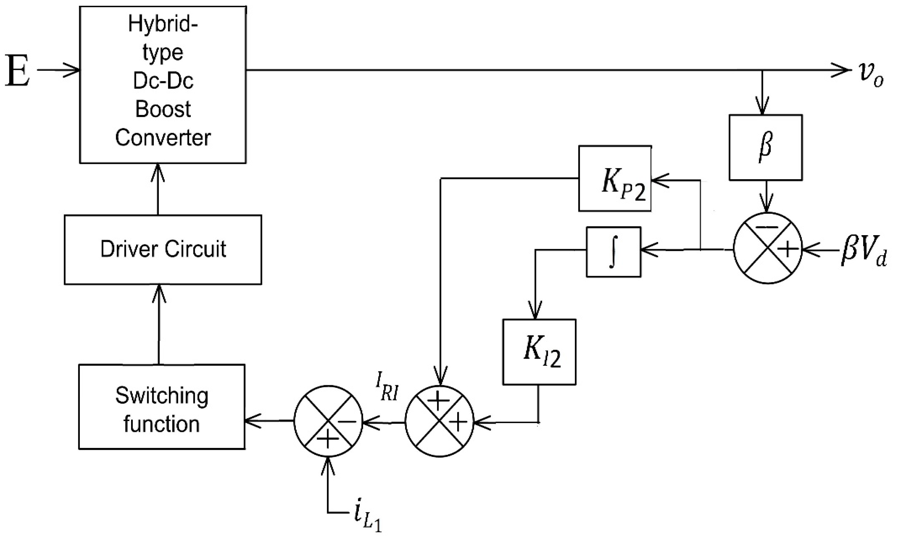
Some experimental as well as simulation outcomes are given to justify the suitability of the SM methodology employing an input current in the feedback. The converter parameters given by (40) were used. The gains of the control scheme employed are K P = 0.1 and K I = 2 . Additionally, the switching function provided by (29) was implemented with δ = 0.1   V , and a voltage feedback factor of β = 0.1 was utilized. The controller’s block schematic is shown in Figure 4.

4.1. Simulation Results

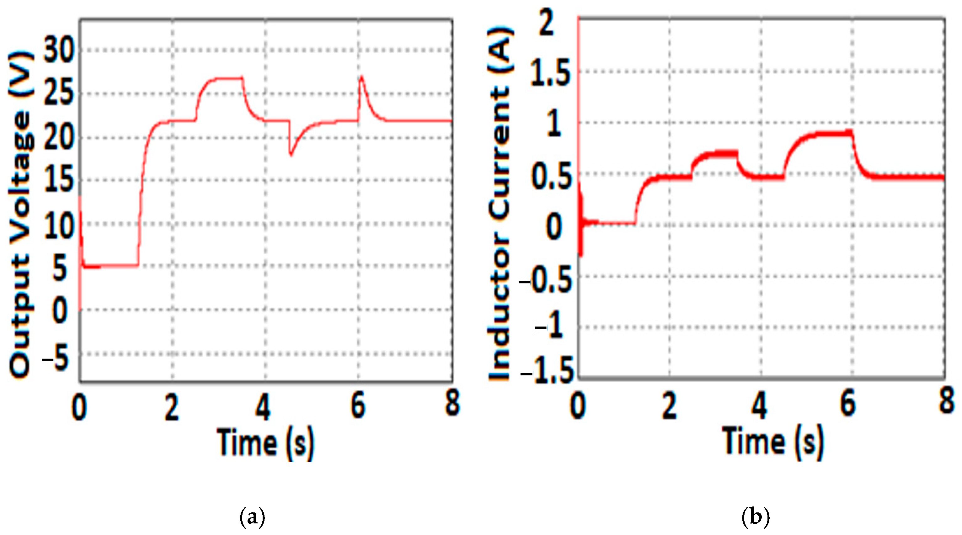
Initially, some simulation outcomes are produced to affirm the analytical outcomes reported in Section 3. To this end, PSIM version 9.0.3 was used to execute the proposed SM-controlled system employing the preferred current through an output inductor [21]. The output voltage and associated current through the inductor of the system are depicted in Figure 5a,b, respectively. At the start, the set point voltage was switched at t = 1 s from 0 V to 21.85 V. Then, at t = 2.5 s, the value of the reference is changed again to 26.85 V, and then at t = 3.5 s, it is changed back to 21.85 V. The system output was seen to keep track of variations in its desired value having almost no overshoot and a very brief settling time, as can be shown. At t = 4.5 s, the load dropped from R = 220 to R = 110 (a 50% reduction), and then at t = 6 sec, it was increased again to R = 220. As can be observed, when load disturbances started, the voltage at the output quickly returned to the chosen reference output voltage.
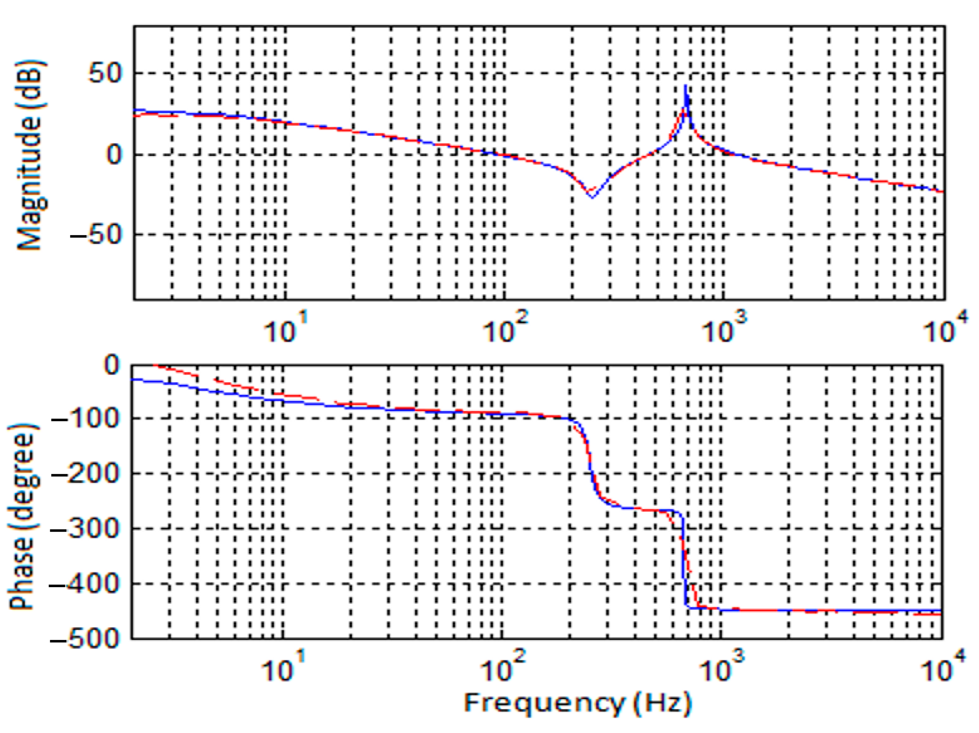
The exactness of the theoretical derivation of the mentioned control scheme presented in this research was then confirmed through a comparison of the analytical and simulated Bode plots of the output voltage to inductor current transfer function. Figure 6 displays the appropriate Bode plots, which were generated using the current in the inductor at the input side in feedback. The transfer function G ~ i I ( s ) = v ~ o ( s ) I ~ R I ( s ) which is given by (41) is depicted by the solid blue line on a Bode plot. Based on the analytical way of the control scheme’s design described in Section 3, this transfer function was obtained. The dotted red waveform depicts the Bode plot based on the actual SM control scheme of the dc-dc converter realized in PSIM software. The PSIM’s ‘AC SWEEP’ technique was used to generate the Bode charts in this case. The AC analysis principle states that a small excitation is introduced at the system’s input end and extracts a signal having the matching frequency at its output end [22]. The analytical design of the suggested controller that controls the dc-dc converter is validated by a satisfactory match between the Bode plot obtained analytically and the same plot produced using the real system’s circuit.

4.2. Experimental Outcomes

Some experimental outcomes are given to justify the suitability of the SM methodology based on an input current in the feedback. The converter parameters given by (40) were used. Also, δ = 0.1   V was employed. Figure 7 shows the circuit schematic of the hardware implementation of the closed-loop scheme. Here, V d s and v 0 s represent scaled values of the reference voltage V d and the output voltage v 0 , respectively, with scaling factor β . The SM controller given by (27)–(29) was built in the laboratory employing routine analog devices as shown in Figure 7. Also, the inductor current was measured using LTS-6NP. The values   K P = 0.1 and K I = 2 were used.
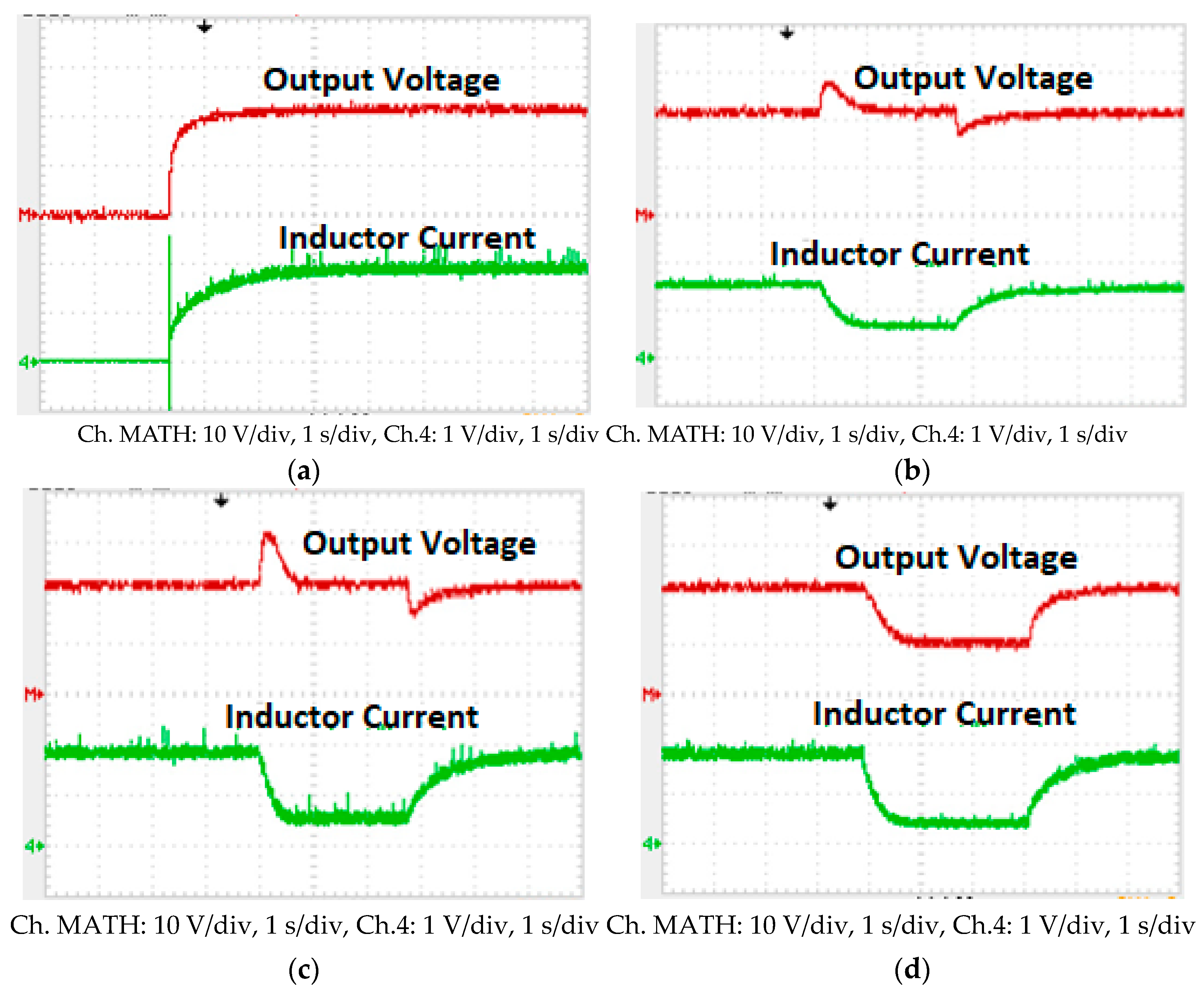
Initially, the system’s transient response is depicted in Figure 8a which demonstrates the waveforms of the voltage at the output and current through an inductor. As demonstrated, a nearly critically damped output response was attained with hardly any overshoot. Figure 8b,c depict the response of the system when the load at the output was changed from 220   Ω to 440   Ω (vice-versa) and 720   Ω (vice-versa), respectively. Once more, it was discovered that the output voltage could be returned to the intended value with a minor overshoot and a worst-case settling time of 0.8 s. It was also assessed how well the suggested controller handled changes in the reference voltage. After switching the reference voltage from V d = 21.85   V to V d = 10.35   V and back again, the converter’s output is shown in Figure 8d. All of these demonstrate the SM controller’s capability to control the output voltage of the system by utilizing the input inductor current.

5. Conclusions

In order to construct the SM scheme for the hybrid step-up configuration, a methodical technique for choosing the best inductor current was described. Two HM-based SM controllers were compared in-depth utilizing two currents through the distinct inductors of the converter. According to the theoretical analysis, the converter’s current-to-output voltage TF is unstable when the SM control scheme uses the inductor current at the output side. The current-to-output TF exhibits unstable pole-zero cancellation. However, the SM scheme utilizing the current through an input-side inductor does not experience this issue. The effectiveness of the HM-based SM control scheme to control the high-order dc-dc converter utilizing the input inductor current was also demonstrated through certain experimental results. Last but not least, it is imperative to highlight that the suggested method for choosing the best state variables is quite general and may be employed to control other high-order step-up topologies by creating workable HM-based SM controllers.

Author Contributions

Conceptualization, S.C.; formal analysis, S.C., M.T., M.A. and R.A.; investigation, S.C. and M.T.; methodology, S.C. and M.T.; validation, S.C.; writing—original draft, S.C.; writing—review and editing, M.T., M.A. and R.A. All authors have read and agreed to the published version of the manuscript.

Funding

This research was supported by Princess Nourah bint Abdulrahman University Researchers Supporting Project Number (PNURSP2023R97), Princess Nourah bint Abdulrahman University, Riyadh, Saudi Arabia.

Acknowledgments

Princess Nourah bint Abdulrahman University Researchers Supporting Project Number (PNURSP2023R97), Princess Nourah bint Abdulrahman University, Riyadh, Saudi Arabia.

Conflicts of Interest

The authors declare no conflict of interest.

References

  1. Axelrod, B.; Berkovich, Y.; Ioinovici, A. Switched-capacitor/switched-inductor Structures for Getting Transformerless Hybrid DC–DC PWM Converters. IEEE Trans. Circuits Syst. I Regul. Pap. 2008, 55, 687–696. [Google Scholar] [CrossRef]
  2. Andrade, P.; Alcaso, A.N.; Bento, F.; Marques Cardoso, A.J. Buck-Boost DC-DC Converters for Fuel Cell Applications in DC Microgrids—State-of-the-Art. Electronics 2022, 11, 3941. [Google Scholar] [CrossRef]
  3. Leyva-Ramos, J.; Ortiz-Lopez, M.G.; Diaz-Saldierna, L.H.; Martinez-Cruz, M. Average current controlled switching regulators with Cascade Boost Converters. IET Power Electron. 2011, 4, 1–10. [Google Scholar] [CrossRef]
  4. Liang, T.-J.; Chen, S.M.; Yang, L.S.; Chen, J.F.; Ioinovici, A. Ultra-large gain step-up switched-capacitor DC-DC converter with coupled inductor for alternative sources of Energy. IEEE Trans. Circuits Syst. I Regul. Pap. 2012, 59, 864–874. [Google Scholar] [CrossRef]
  5. Morales-Saldaña, J.A.; Galarza-Quirino, R.; Leyva-Ramos, J.; Carbajal-Gutiérrez, E.E.; Ortiz-Lopez, M.G. Multiloop controller design for a quadratic boost converter. IET Electr. Power Appl. 2007, 1, 362–367. [Google Scholar] [CrossRef]
  6. Chincholkar, S.H.; Chan, C. Investigation of current-mode controlled Cascade Boost converter systems: Dynamics and stability issues. IET Power Electron. 2016, 9, 911–920. [Google Scholar]
  7. Chan, C.-Y.; Chincholkar, S.H.; Jiang, W. Adaptive current-mode control of a high step-up DC–DC converter. IEEE Trans. Power Electron. 2017, 32, 7297–7305. [Google Scholar] [CrossRef]
  8. Dupont, F.H.; Rech, C.; Gules, R.; Pinheiro, J.R. Reduced-order model and control approach for the boost converter with a voltage multiplier cell. IEEE Trans. Power Electron. 2013, 28, 3395–3404. [Google Scholar] [CrossRef]
  9. Chincholkar, S.H.; Chan, C.-Y. Design of fixed-frequency pulsewidth-modulation-based sliding-mode controllers for the quadratic boost converter. IEEE Trans. Circuits Syst. II Express Briefs 2017, 64, 51–55. [Google Scholar] [CrossRef]
  10. He, Y.; Luo, F.L. Sliding-mode control for DC–DC converters with constant switching frequency. IEE Proc. Control Theory Appl. 2006, 153, 37–45. [Google Scholar] [CrossRef]
  11. Tan, S.-C.; Lai, Y.M. Constant-frequency reduced-state sliding mode current Controller for Cuk converters. IET Power Electron. 2008, 1, 466–477. [Google Scholar] [CrossRef]
  12. Tan, S.C.; Lai, Y.M.; Tse, C.K. Indirect sliding mode control of power converters via double integral sliding surface. IEEE Trans. Power Electron. 2008, 23, 600–611. [Google Scholar] [CrossRef] [Green Version]
  13. Chincholkar, S.H.; Jiang, W.; Chan, C.-Y. An improved PWM-based sliding-mode controller for a DC–DC cascade boost converter. IEEE Trans. Circuits Syst. II Express Briefs 2018, 65, 1639–1643. [Google Scholar] [CrossRef]
  14. Lopez-Santos, O.; Martinez-Salamero, L.; Garcia, G.; Valderrama-Blavi, H.; Sierra-Polanco, T. Robust sliding-mode control design for a voltage regulated quadratic boost converter. IEEE Trans. Power Electron. 2015, 30, 2313–2327. [Google Scholar] [CrossRef]
  15. López-Santos, O.; Martínez-Salamero, L.; García, G.; Valderrama-Blavi, H.; Mercuri, D.O. Efficiency analysis of a sliding-mode controlled quadratic boost converter. IET Power Electron. 2013, 6, 364–373. [Google Scholar] [CrossRef]
  16. Chincholkar, S.H.; Jiang, W.; Chan, C.-Y. A normalized output error-based sliding-mode controller for the DC–DC cascade boost converter. IEEE Trans. Circuits Syst. II Express Briefs 2020, 67, 92–96. [Google Scholar] [CrossRef]
  17. Chincholkar, S.H.; Jiang, W.; Chan, C.-Y. A modified hysteresis-modulation-based sliding mode control for improved performance in hybrid DC–DC boost converter. IEEE Trans. Circuits Syst. II Express Briefs 2018, 65, 1683–1687. [Google Scholar] [CrossRef]
  18. Górecki, P.; Górecki, K. Methods of Fast Analysis of DC–DC Converters—A Review. Electronics 2021, 10, 2920. [Google Scholar] [CrossRef]
  19. Doyle, J.C.; Francis, B.A.; Tannenbaum, A. Feedback Control Theory; Dover: Mineola, NY, USA, 1990. [Google Scholar]
  20. Åström, K.J.; Murray, R.M. Feedback Systems; Princton University Press: Princeton, NJ, USA, 2008. [Google Scholar]
  21. Powersim Inc. Available online: https://powersimtech.com/wp-content/uploads/2021/01/PSIM-User-Manual.pdf (accessed on 3 August 2023).
  22. Powersim Inc. Available online: https://powersimtech.com/resources/tutorials/how-to-perform-an-ac-sweep-with-psim/ (accessed on 3 August 2023).
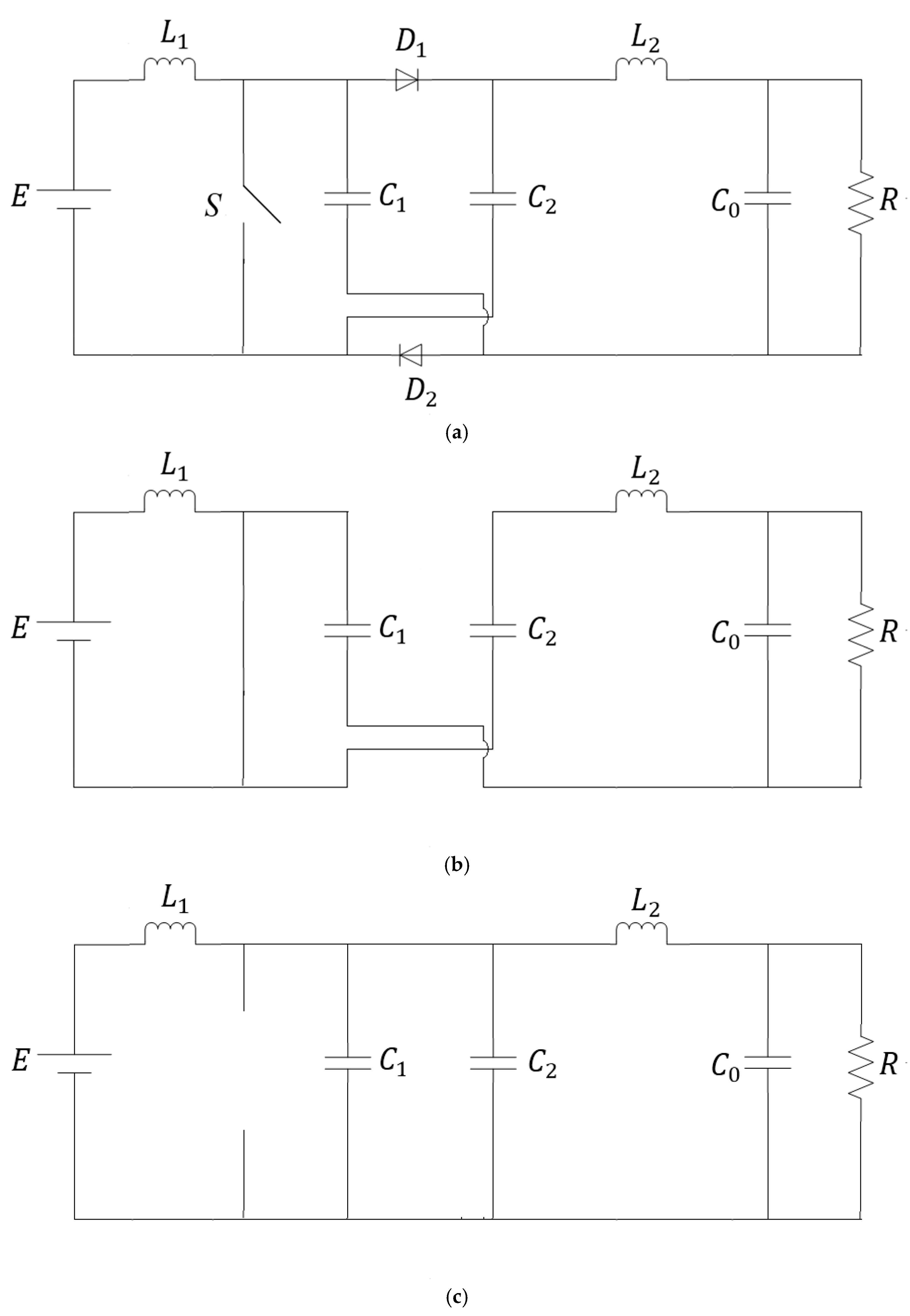
Figure 1. Circuit diagram and modes of operation of the hybrid topology: (a) circuit schematic; (b) u = 1 ; (c) u = 0 .
Information 14 00443 g001
Figure 2. A two-loop control scheme.
Information 14 00443 g002
Figure 3. Bode plot of loop gain G L s obtained with a SM controller based on an input current in the feedback.
Information 14 00443 g003
Figure 4. Controller’s block schematic.
Information 14 00443 g004
Figure 5. System’s response employing the input inductor current: (a) the response of the output voltage for load and reference voltage disturbances; (b) the corresponding waveform of the inductor current.
Information 14 00443 g005
Figure 6. Bode plot of the transfer function (31). Solid blue line: Bode plot based on the analytical approach of the design of the control scheme. Dotted red line: Bode plot based on the actual SM control scheme for the dc-dc converter realized in PSIM software.
Information 14 00443 g006
Figure 7. The circuit schematic of the hardware implementation of the closed-loop scheme.
Information 14 00443 g007
Figure 8. System response obtained with the SM methodology based on current through the input-side inductor (top red waveform: output voltage (Ch. MATH: 10 V/div, 1 s/div), and bottom green waveform: current through input-side inductor (Ch.4: 1 V/div, 1 s/div)): (a) converter’s transient response. (b) Waveforms when load varied from 220   Ω to 440   Ω and vice-versa. (c) Waveforms when load varied from 220   Ω to 720   Ω and vice versa. (d) Waveforms when reference input changed from 21.85   V to 10.35   V and then back to 21.85   V .
Information 14 00443 g008
Disclaimer/Publisher’s Note: The statements, opinions and data contained in all publications are solely those of the individual author(s) and contributor(s) and not of MDPI and/or the editor(s). MDPI and/or the editor(s) disclaim responsibility for any injury to people or property resulting from any ideas, methods, instructions or products referred to in the content.