Article

FPGA Implementation of Crossover Module of Genetic Algorithm

1
Department of Electrical and Computer Engineering, University of Victoria, Victoria, BC V8W 2Y2, Canada
2
Department of Computer Engineering, Princess Sumaya University for Technology, P.O. Box 1438, Al-Jubeiha, Amman 11941, Jordan
*
Author to whom correspondence should be addressed.
Information 2019, 10(6), 184; https://doi.org/10.3390/info10060184
Submission received: 3 April 2019 / Revised: 22 May 2019 / Accepted: 23 May 2019 / Published: 28 May 2019

Abstract

:
This paper proposes a hardware realization of the crossover module in the genetic algorithm for the travelling salesman problem (TSP). In order to enhance performance, we employ a combination of pipelining and parallelization with a genetic algorithm (GA) processor to improve processing speed, as compared to software implementation. Simulation results showed that the proposed architecture is six times faster than the similar existing architecture. The presented field-programmable gate array (FPGA) implementation of PMX crossover operator is more than 400 times faster than in software.

1. Introduction

1.1. Genetic Algorithm

Genetic algorithm (GA) is a robust stochastic optimization technique that is based on the principle of survival of the fittest in nature. The GA has an ability to provide optimum solution to a wide range of problems. GA starts from the initial population of randomly generated individuals, each of which is an encoding of a solution to the problem. The overall rule for how to select parents from the population for reproduction is survival of the fittest. Individuals are chosen to mate with probability proportional to their fitness. GA evolves the population over generations using crossover and mutation operations. Crossover operator has a role in the extraction of good characteristics from both parents [1] and the mutation is used to avoid converging to local optimal. In each iteration, the termination criterion is checked and if it is reached, the whole GA procedure stopped. The two main criteria to evaluate the effectiveness and terminate the GA are the maximum number of generations and a satisfactory fitness value.

1.2. Hardware Implementation of GA

As GA is very effective in solving many practical problems, speeding up its time-consuming operators is important in its applications [2]. The need for hardware implementation of GA arises from the massive computational complexity of the algorithm that incurs delay to the execution of GA implementation in software. Since the GA modules are intrinsically parallel algorithms and the basic operations of a GA can be executed in a pipelining fashion, speed up could be achieved when they are implemented in hardware, including with Field-Programmable Gate Array (FPGA) [3]. One of the main advantages of FPGAs is that they are compatible with pipelined and parallel architectures that can lead to high computing performance. In this paper, the associative cache mapping technique is used for parallelization. In this cache mapping technique, the tag bits of an address received from the processor are compared to the tag bits of each block of the cache to see whether the desired block is present. We discuss, in the next sections, how this technique is used to perform comparisons in parallel.

1.3. Travelling Salesman Problem

The TSP is the problem of a salesman who aims to find the shortest possible path to visit a specified set of cities without repeating. Many practical applications require the modelling and solving TSP, such as overhauling gas turbine engines, computer wiring, the order-picking problem in warehouses, vehicle routing, mask plotting in PCB production, distribution system, X-ray crystallography, job scheduling, circuit board drilling, and DNA mapping [4]. As TSP is an NP-hard (nondeterministic polynomial time) problem in combinatorial optimization, it has a large solution space, thus it is necessary to use heuristic searching methods. GA is one of the many alternatives that our results show that is not well suited to TSP. In this age, neural networks (NNs) are more popular than GA, but GAs are still used because NNs require a lot of data, while GAs do not [5].

1.4. Importance of Crossover Module in GA

Generally, the GA modules in terms of high computation complexity and hence long execution time are in the following descending order: Fitness function, crossover and selection, mutation and breeding, and initial population. The crossover module plays a larger part in computational complexity (from the hardware perspective) and accuracy (from the software perspective) as compared to the other modules. Therefore, the main goal of this work is FPGA implementation of the crossover module in GA to solve TSP. The fitness value of a chromosome in TSP can be calculated as simply the total distance to travel to all the cities in the specified order. Therefore, it can be implemented using a simple circuit and there is no computational complexity.
What makes our proposed architecture unique, compared to previous works, is that we use only two memories to store the parents and children, which results in reducing the number of required flip flops by half. Moreover, the associative cache mapping technique is used for processing parallelization, thus speeding up the processing time.
The rest of the paper is organized as follows. Section 2 gives a brief introduction to partially-mapped crossover technique and surveys previous related works. In Section 3, we first briefly discuss the challenges in hardware implementation of GA and then describe in detail the design methodology and the hardware implementation details of the proposed crossover module. Section 4 reports the simulation results at various design sizes to verify the functionality of the designed module. The paper will conclude with a summary of our results and a discussion of future plans.

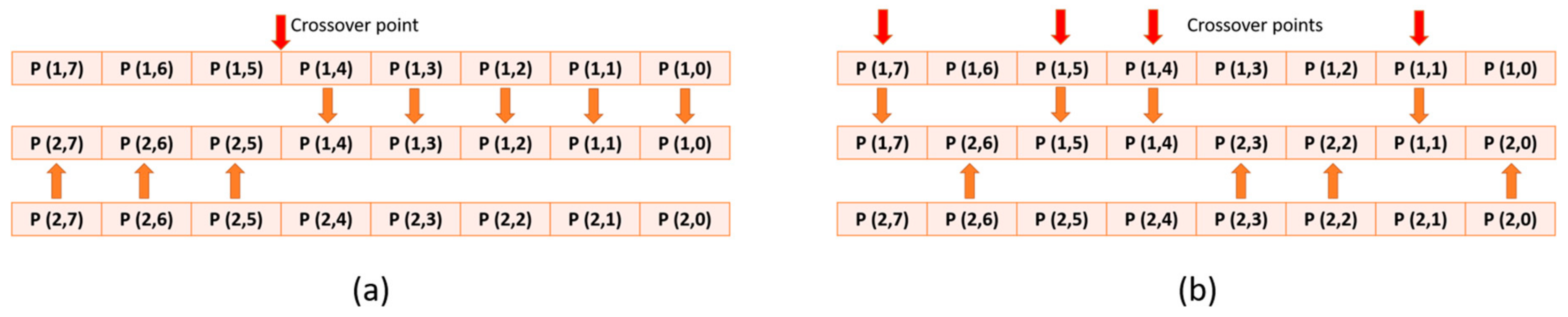
2. Crossover Technique and Related Work

2.1. Existing Work in Hardware Implementation of Crossover Module

In Reference [6], the crossover operators are classified into three categories such as standard crossovers, binary crossovers, and real/tree crossovers, which are application dependent. Various crossover techniques are implemented in hardware for different applications to speed up the computation, as compared to software. In order to get some ideas about the hardware implementation of crossover, we have investigated some different crossover architectures. The following is a brief survey of existing hardware designs of crossover that shows how different crossover techniques can be implemented.
In Reference [7], a GA engine is proposed that supports one-point and two-point crossovers. The proposed GA processor in Reference [8] has three methods of crossover including one-point, two-point, and uniform crossovers.
A parallel GA system on four Virtex-6 FPGA is proposed in Reference [9]. Since the selection, crossover and mutation operators deal with two individuals sequentially to generate a new offspring, these operators are combined in a unit to increase the performance. Their system supports different crossover methods for different problems including one-point crossover for binary chromosomes, multiple-point crossover for permutation chromosomes, and blending crossover for real-valued chromosomes.
In Reference [10], the adaptive GA is designed on FPGA, based on modular design that supports two-point crossover. Figure 1 shows two crossover methods provided in Reference [11], named as one-point and multi-point crossover.
The crossover module of [12] implements single point crossover. As seen in Figure 2, the architecture consists of four bit splitters (CMDIV), two identical crossover submodules (CMPQ), and two concatenators (CMCCAT). After the two input chromosomes are split into two halves using CMDIV modules, the crossing is performed in CMPQ modules. Then, the least significant half of the variables will be concatenated to generate one new chromosome and the same procedure is applied to the most significant halves to generate the other chromosome.

2.2. Existing Work in Hardware Implementation of Partially-Mapped Crossover (PMX) Technique

The selection of the crossover operator plays an important role on the performance of GA. The crossover technique used in this implementation is Partially-Mapped Crossover (PMX). It begins by picking two random cut points along the parent strings. In the first step, the segments between the cut points are copied from the parent 1 to the offspring 2 and from the parent 2 to the offspring 1. A series of mapping is also defined based on these segments. In the next step, all the elements before the first cut point and after the second one are copied from the parent 1 and parent 2 to the offspring 1 and offspring 2, respectively. However, in TSP problem, this operation might result in an invalid tour because an offspring may get duplicate cities. In order to overcome generating an invalid tour, if a number is already present in the offspring, it is replaced according to the previously defined series of mappings. For example, given two parents with cut points marked by vertical lines: p1= (3 | 0 1 4 5 | 2) and p2= (2 | 1 3 5 4 | 0) the PMX operator will define the series of mappings (0↔1, 1↔3, 4↔5) and produce the following offspring: o1= (0 | 1 3 5 4 | 2) and o2= (2 | 0 1 4 5 | 3).
Since, in this paper, PMX crossover technique is investigated, the following is a detailed review of PMX implementation. In Reference [5], the GA algorithm is implemented in a software application developed in C++ language and only the crossover module is implemented in FPGA. The proposed architecture of crossover circuit is depicted in Figure 3. As we compare our results to this work in Section 4, we will discuss their proposed architecture in more details. Two special 10-bit registers store the cut points are randomly chosen by the software application. The actual length of a tour in TSP problem is stored in the Max register in Figure 3. The architecture supports tours composed of, at most, 1024 cities, therefore, there are four memories of size 10 × 210 to keep parent and offspring samples. In order to performing the crossover operation, four additional memories are used. These memories are complex maps and simple maps that are shown in Figure 3: “CM1” and “CM2” of size 10 × 210 and “SM1” and “SM2” of size 1 × 210. Every time a city is written to parent memories, the simple maps will be reset. After that, the segments between the cut points are swapped. Each time a city c1 from the “Parent 1” is transferred to the “Offspring 2”, a value “1” is written to the simple map “SM2” at the address c1. The same thing occurs with the second parent and “SM1”. At the same time, the value c1 and c2 are stored at the address c2 and c1 in the complex map “CM1” and “CM2”, respectively. The next step is copying all the cities before the first cut point and after the second cut point from the “Parent 1” to the “Offspring 1” and from the “Parent 2” to the “Offspring 2”, and if there is any repeating cities, it must be resolved. After a city c is read from the “Parent 1”, the value of address c in “SM1” should be checked. If this value is “0”, then this city can be copied to the “Offspring 1”, and if this value is “1”, it means that “Offspring 1” has already included this city. In order to replace it with some other cities, the complex map “CM1” is employed, as shown in the flow-chart in Figure 4.
Another hardware implementation of PMX crossover is presented in [13]. As is shown in Figure 5, in their architecture, cross-bit are set to No. 9 and No. 17, that is the binary code of the 4th, 5th, and 6th city counted from the right side of the code. The 9th to 17th bits of individual are put into the left of b individual, and b into a, and then the repetitious city serial number is removed from the original one.

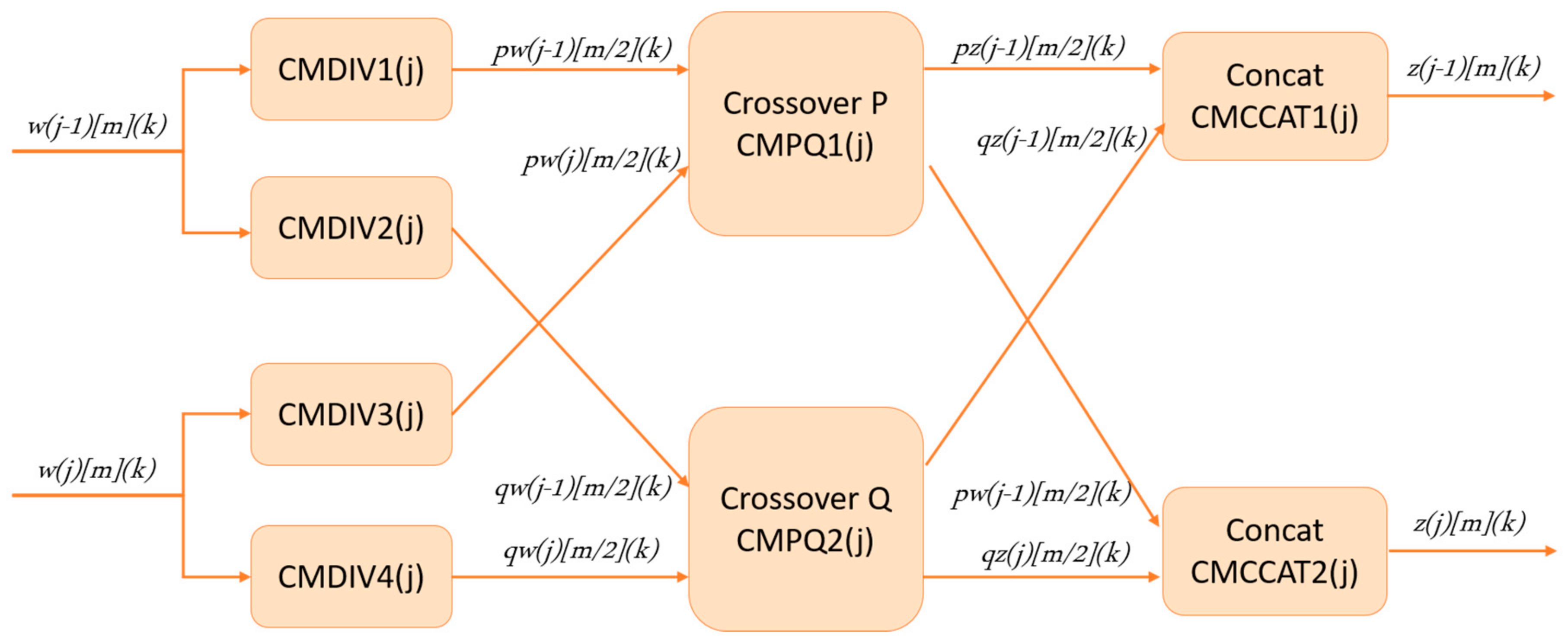
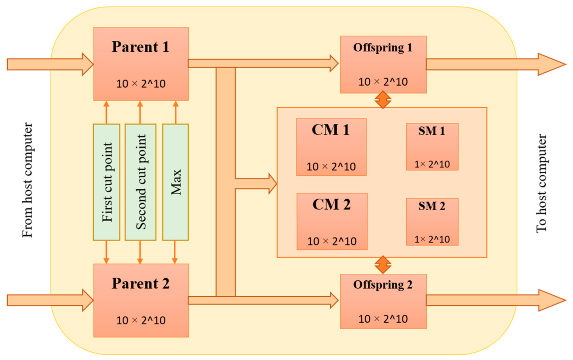
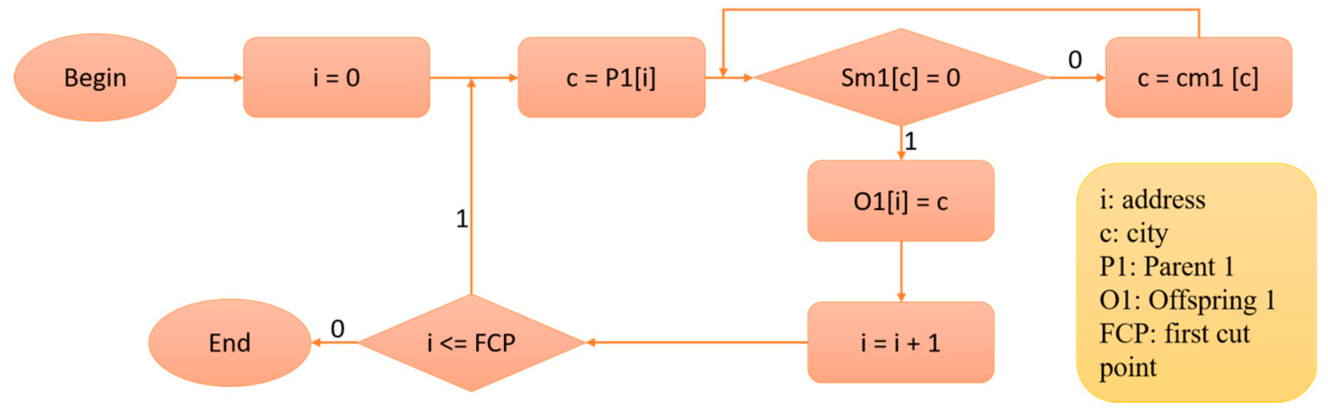
3. Hardware Implementation

3.1. Challenges in Hardware Implementation of GA

There are three main challenges in FPGA implementation of GA including the data flow, the amount of hardware resources and the size of memory. Since different operations should be done on one set of data, a lot of data will need to be accessed from different operational modules and control logic would require lines to all modules’ inputs. Since GA requires a modular architecture, this would pose a long routing on FPGA. The hardware ability to parallelize offer great opportunities to speed up GA operation, but the amount of hardware resources needed in such a hardware solution is another important constraint for hardware implementation. This kind of hardware solution may become too costly, and hence much less practical to use. Since GA requires a large memory to store the input netlist and intermediate population, the size of required memory is a bottleneck. In this paper, in order to achieve improvement in processing speed and hardware features of the implemented architecture, we aimed to reduce the size of memories and shorten the paths in data flow. As can be seen in Section 2, in most of the hardware implementations of the crossover module, four memories are used to keep parent and offspring samples, but we propose and manage to use only two memories to store the parents and children. Some temporary registers are used to facilitate the generation of children. Moreover, the associative cache mapping technique is used for parallelization and speed up of the processing time, to be discussed in details in the following subsection.

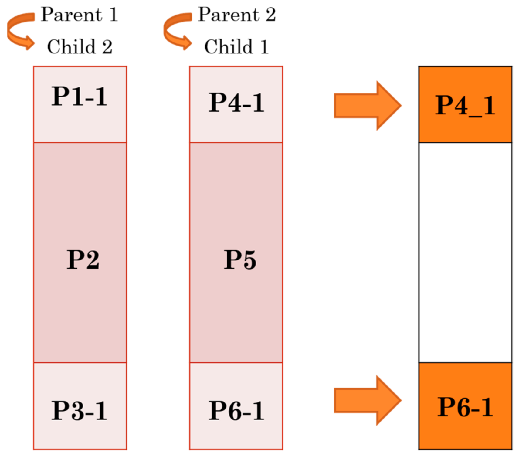
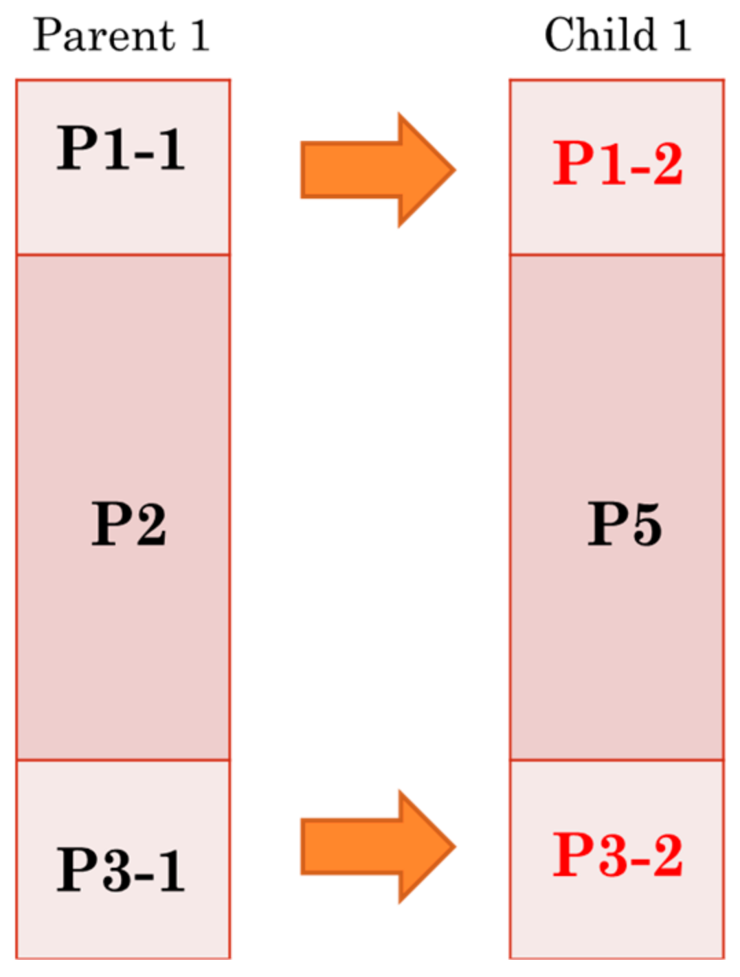
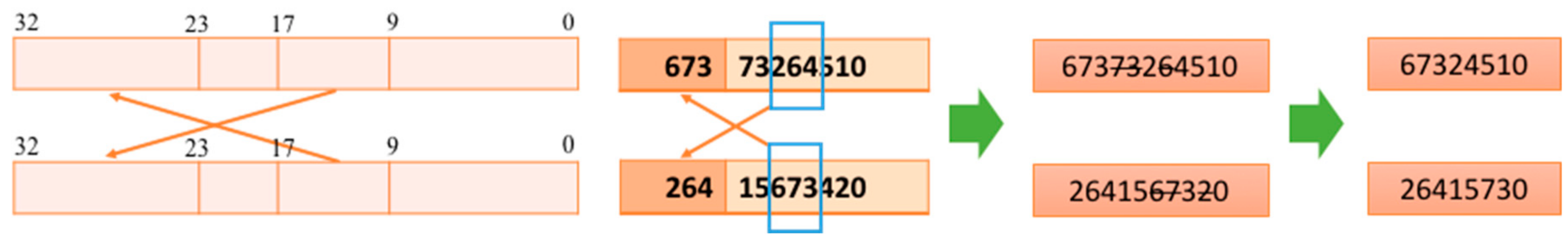
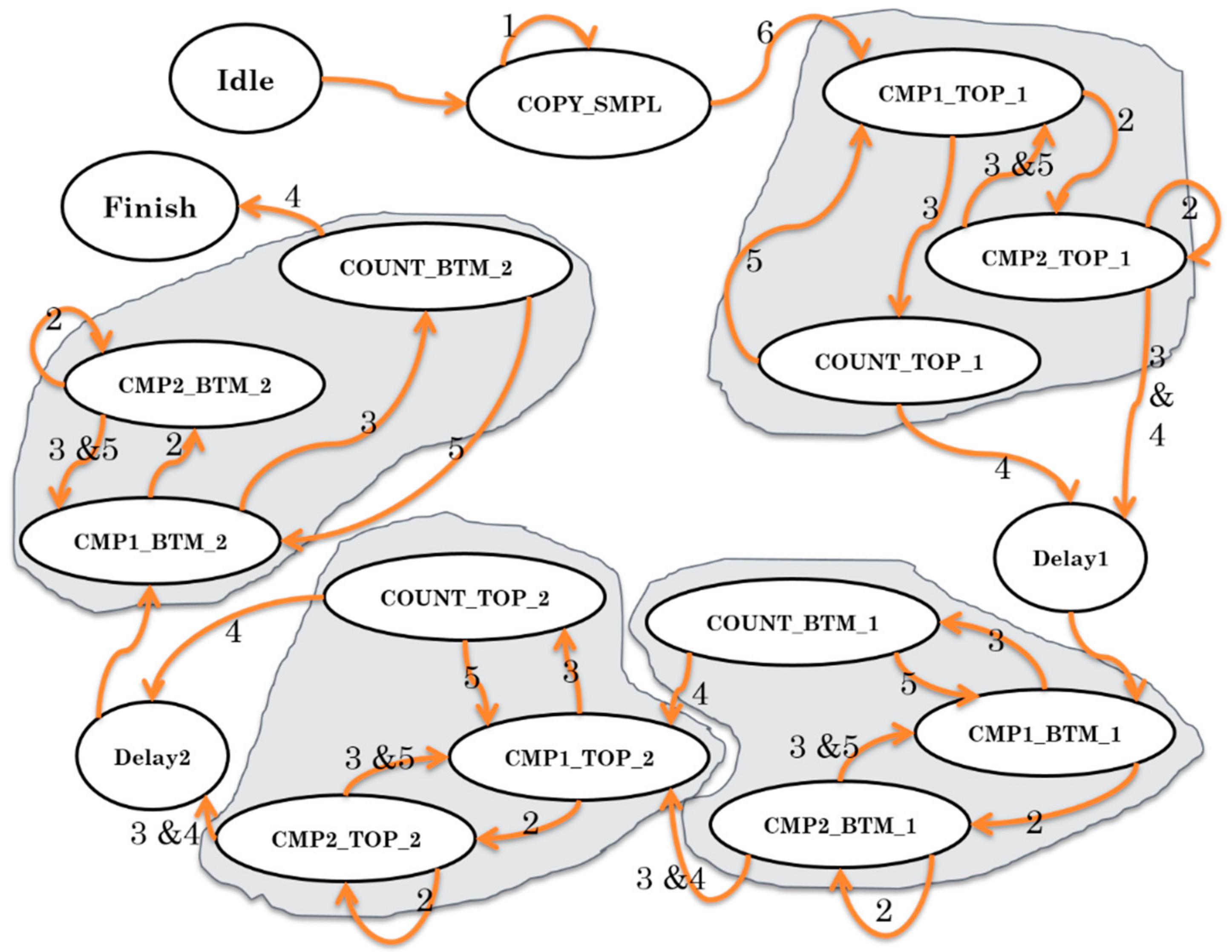
3.2. Proposed Architecture for PMX Crossover Module

The overall architecture of this work can be divided into two main parts including memories and control logic. In this subsection, we introduce and discuss the design modules in details. Two memories are provided to store parents and generated children. In the control logic, the main part is a state machine. Besides, in order to speed up generating children using associative cache mapping technique, the number of chromosomes determines the number of comparators. Moreover, there are three counters to control loops and some multiplexers.
The main concept of our proposal is shown in Figure 6, Figure 7 and Figure 8. The children are generated in the same memories that parents are stored. As can be seen in Figure 6, child 1 and 2 are generated in parent 2 and 1 memories, respectively. First, child 1 is generated in parent 2 so it needs to store parts P4-1 and P6-1 in two temporary memories.
In the next step, parts P1-2 and P3-2 will be filled up by copying the elements of the parts P1-1 and P3-1, respectively. After this step, child 1 is ready. In order to eliminate redundancy in the generated chromosomes, some logics are implemented that will be discussed in the following sections.
As illustrated in Figure 8, parts P4-2 and P6-2 will be filled up by the elements of the parts P4-1 and P6-1, respectively.
The main part of the control logic in this architecture is a state machine as shown in Figure 9. Moreover, there are three counters to control loops and some multiplexers. Counter k counts the elements that are compared and copied from parts P1-1, P3-1, P4-1, and P6-1 to the parts P1-2, P3-2, P4-2, and P6-2, respectively.
The designed state machine works as follows. After activation, it enters the COPY_SMPL state to copy part P4-1 and part P6-1 into the temporary memory as shown in Figure 6. Top and bottom of the temporary memory are initialized in parallel. The state machine stays in this state until the temporary memory is filled up. After that, we need to generate parts P1-2, P3-2, P4-2, and P6-2, respectively. To generate each part, three states are considered: CMP1, CMP2, and COUNT. For parts P1-2 and P4-2 that are located on the top of the chromosomes, these states are named TOP and for parts P3-2 and P6-2 that are located on the bottom of the chromosomes, these states are named BTM. Based on how many repeated genes there are in each part, the state machine transits between states. Table 1 shows the state transition triggering events of the state machine. In the proposed architecture, if there are m cities in each chromosome, m comparators are implemented to compare parent and children’s genes. These comparators are used to overcome generating invalid tour and finding mapping pattern.
In order to implement comparators’ logic, the associative cache mapping technique is used. This cache mapping method is based on parallel comparison of tag bits of the cache to see if the tag bit of an address received from the processor is present. Cost of an associated mapped cache is high because it needs to search all the tag patterns to determine whether a block is in cache, and this infers high hardware cost. In our implementation, this technique works as follows. For example, for filling up part P1-2 using elements of the part P1-1, sample i of P1-1 is compared to all elements of P5. If it is equal to none of them, it is copied to the address i of part P1-2. Otherwise, it is replaced according to the mapping procedure we explain above.

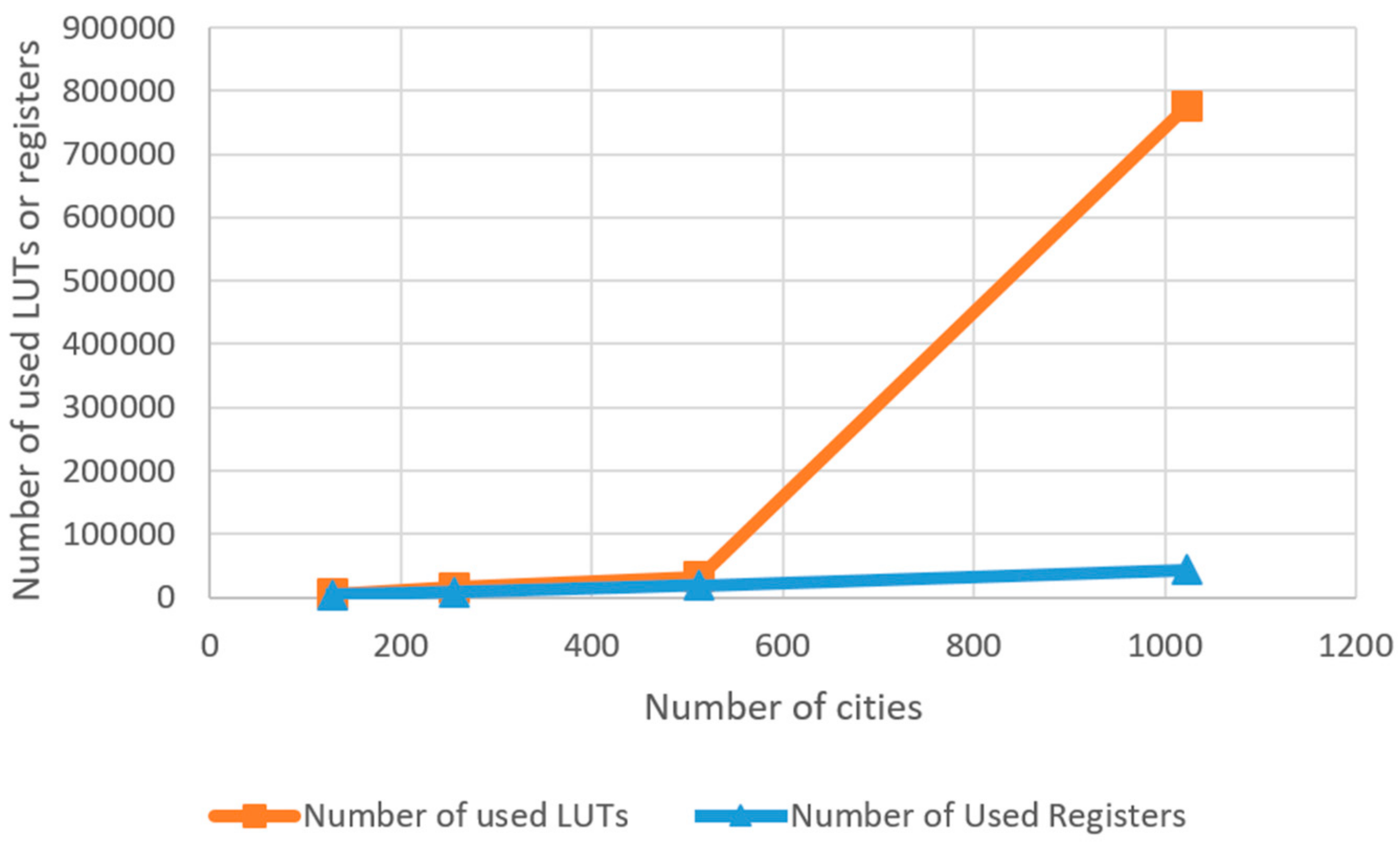
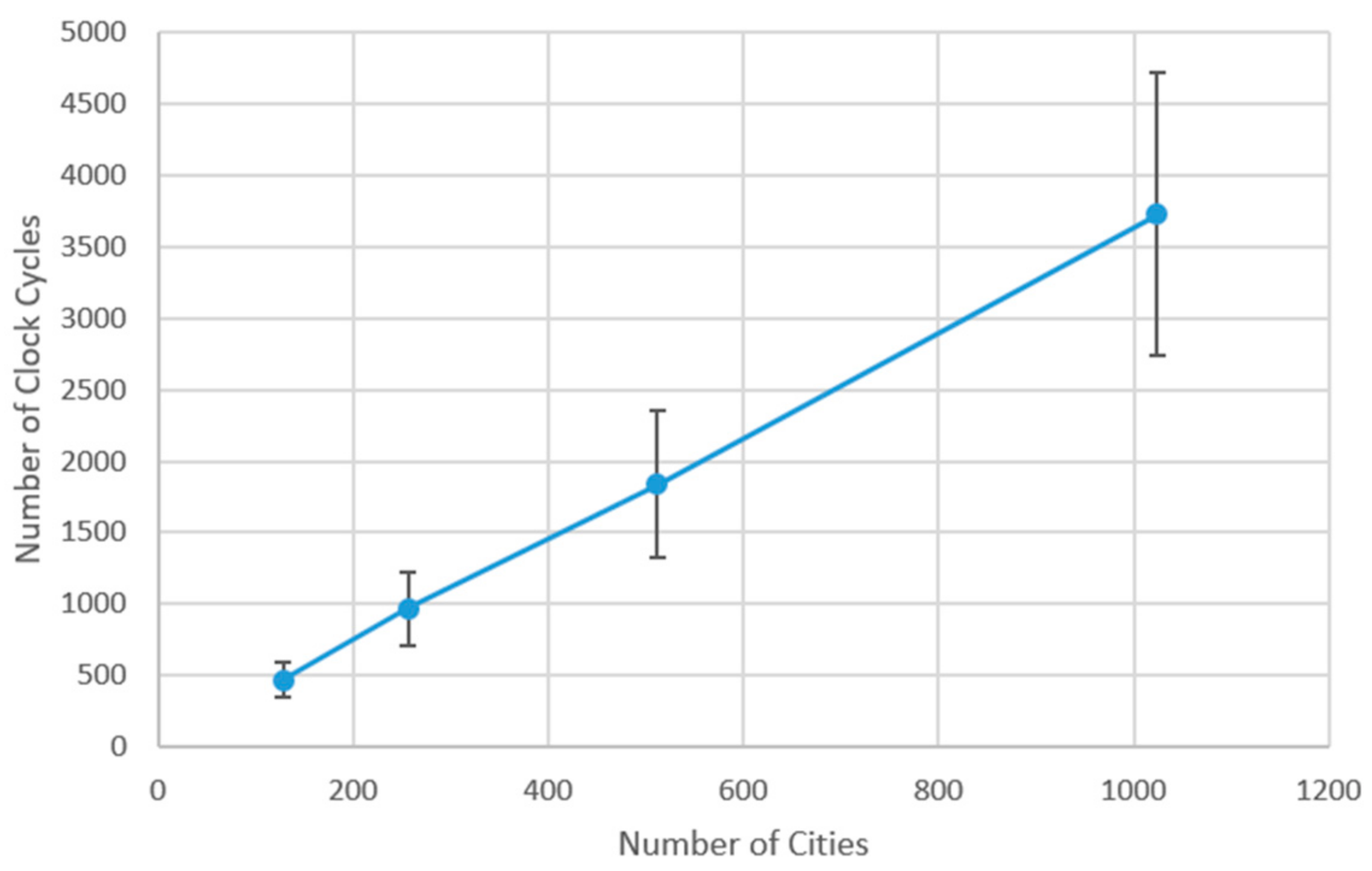
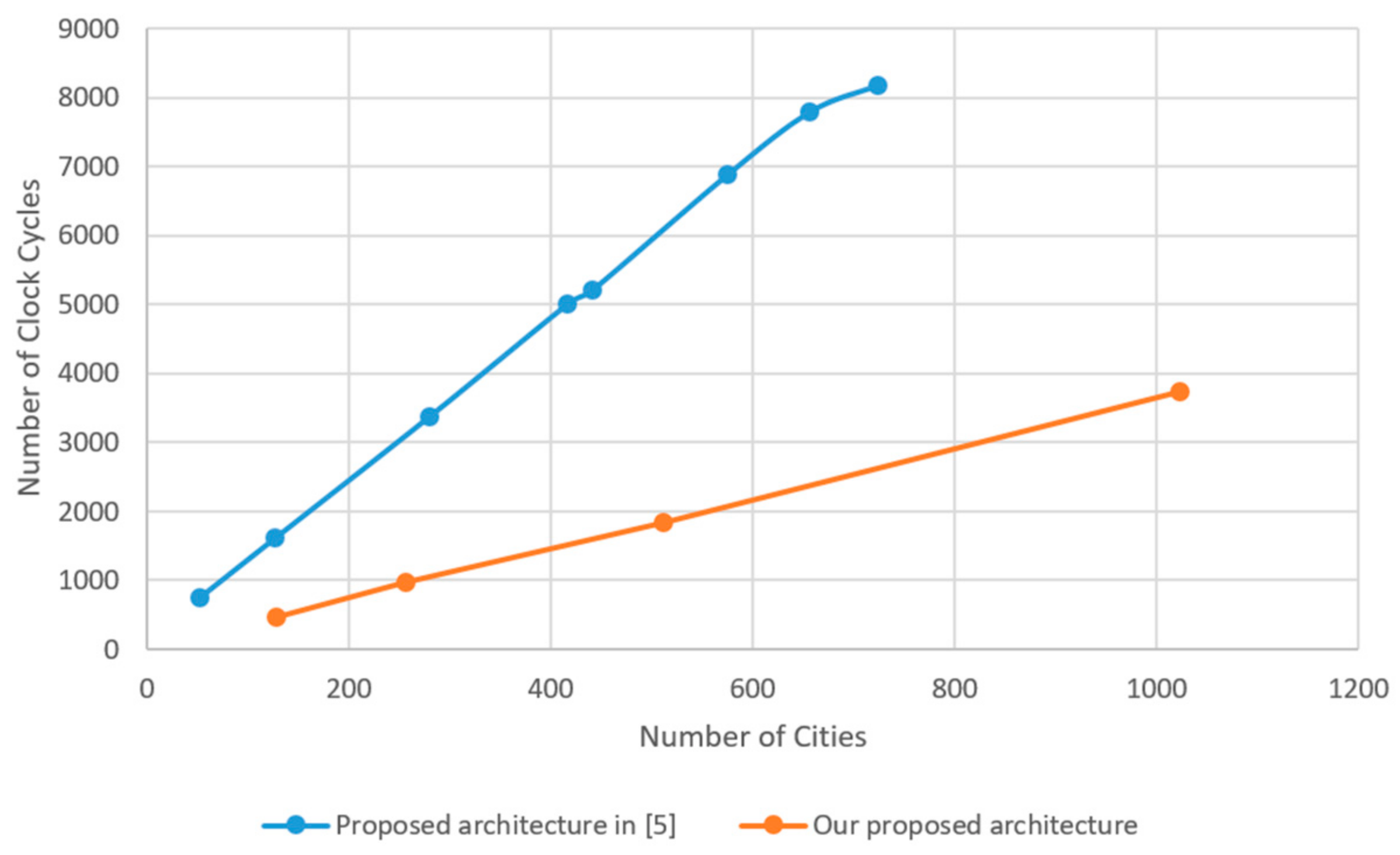
4. Experimental Results and Comparison

Since most of the existing hardware implementations are complete GA algorithm [9,11,12], they reported the quality of solutions and the search speed as performance metrics, so, there is no crossover performance evaluation individually and independently. Whereas detailed information of crossover module is presented only in Reference [5], therefore, we can only compare our simulation results with the reported results of that work. As we compare our implementation to the one proposed in Reference [5], from now on we refer to it as the baseline architecture.
In almost all of the related works, RAM_block is used to store parent and offspring samples. In our proposed architecture associative cache mapping technique is used to speed up the comparisons, so memories cannot be implemented using RAM_blocks, therefore, we have used flip flops to store parent samples. Thus, in order to have a fair comparison, we calculate the number of required flip flops. If there are m cities in each chromosome, each sample is presented using [ log 2 m ] + 1 number of bits. As a result, the size of each memory (to store each parent) and the temporary memory are equal to m × [ log 2 m ] + 1 . As can be inferred from the proposed architecture, the total number of flip flops is equal to 3 m × ( [ log 2 m ] + 1 ) . In a similar way, we can calculate the total number of flip flops for the baseline architecture, which is ( 2 + 6 m ) × ( [ log 2 m ] + 1 ). Thus, the number of flip flops used in our proposed architecture is less than half of what is used in the baseline architecture.
We used Virtex 7 FPGA in our simulations while in the baseline architecture, Virtex E FPGA is used as the hardware platform that we do not have access to, so that we cannot simulate our implementation using the same platform. Since slice structure of different FPGAs are not the same, comparing the number of slices is not fair. Therefore, we need a fair method for area comparison. While Look Up Tables (LUT) are not the same in different FPGAs, comparing the number of LUTs is the fairest available approach. Each slice of Virtex E contains two LUTs. As is reported in baseline architecture, the total number of slices utilized is 149 so the number of LUTs are 298. Table 2 shows implementation results. As can be seen, the proposed architecture has satisfactory results in all cases except 1024 cities, where the problem becomes too complex due to high parallelization for the simulator to handle. Figure 10 shows the number of used registers and LUTs for our proposed architecture. As mentioned previously, our main goal is to improve the processing speed and since we are comparing two hardware implementations, there is a tradeoff between speed and area; it makes sense that we have obtained higher speed at the expense of the larger area. The large number of comparators in our architecture imposes area constraint, and the maximum size that can be implemented is 1024.
Since the number of clock cycles in our proposed architecture is strongly dependent on cut points chosen and mapping pattern, it is not a fixed number for each size of chromosome. To apply mapping pattern, in addition to memory reading/writing operations, some comparisons are needed to ensure only valid tours are constructed. As a result, the greater distance between the cut points results in a faster completion of the PMX crossover in FPGA. So in order to evaluate the speed of the design, 20 samples with different conditions are run for each size of chromosome and the arithmetic average and standard deviation of them are shown in Figure 11. As can be seen, it has a linear trend with acceptable deviation.
To draw a speed comparison between baseline and our architecture, we consider the hardware speed and how much speedup is obtained as compared to the software. The number of clock cycles for baseline and our proposed architecture are depicted in Figure 12. The speedup for different size of chromosomes are not the same. As can be seen, by size increasing, our proposed design performs much faster. Based on what is reported in Reference [5], the average number of clock cycles for performing the crossover in software is equal to 2,486,190. The software version was based on the C++ language and executed on a PentiumIII/800MHz/256MB running Windows2000. Average speedup of the baseline and our architecture, as compared to the software are 22.8 and 1338, respectively. As can be seen, crossover operator is executed in FPGA much faster than in software and our design speedup is around 60 times more than baseline implementation. Since simulation shows no promising results, we did not pursue the actual implementation on FPGA for further investigation.
To study the effect of comparator count on the area and speed, we decreased the number of comparators by 75% and comparisons are done serially. To perform the same number of comparisons, the remaining comparator logics had to be utilized multiple (depending on the cut points) times in a serial manner. The serialization of the comparison operations negatively affected the speed which was expected. Surprisingly, the area increased by 40% as well. We suspect that the extra logic needed to implement the serialization logic causes the area overhead. This shows that the main architecture is more optimized regarding area and speed.

5. Conclusions and Future Work

In this paper we presented a hardware implementation of Crossover module to solve TSP. In order to decrease processing speed, as compared to software implementation, we used the associative cache mapping technique. As a result of utilizing this technique, our proposed architecture is around 2.7 times faster in hardware and around 60 times faster in software rather than the architecture proposed in Reference [5]. The results of experiments showed that the proposed architecture of PMX crossover operator is executed in FPGA more than 1300 times faster than in software. As the proposed architecture utilizes large scale parallelization, no result is obtained in terms of area requirement for a larger number of cities. However, it is well suited for real time applications like fog and cloud computing and scheduling [14], where the number of cities is typically smaller.
In this project only the crossover module of GA is implemented. Possible future work involves implementation of the other modules and evaluation of the complete system. Another interesting future direction would be hardware implementation of the other crossover techniques and comparing them in terms of processing speed, size of required memories, and resource utilization.

Author Contributions

Conceptualization, A.K.; Formal analysis, N.A.; Funding acquisition, K.F.L.; Investigation, Narges Attarmoghaddam and K.F.L.; Methodology, N.A. and A.K.; Project administration, A.K.; Supervision, K.F.L.; Writing—original draft, N.A.; Writing—review & editing, K.F.L.

Funding

This research was funded by Natural Sciences and Engineering Research Council of Canada: Discovery grant number 36401.

Conflicts of Interest

The authors declare no conflict of interest.

References

  1. Gallard, R.H.; Esquivel, S.C. Enhancing evolutionary algorithms through recombination and parallelism. J. Comput. Sci. Technol. 2001, 1. Available online: http://sedici.unlp.edu.ar/bitstream/handle/10915/9423/Documento_completo.pdf?sequence=1&isAllowed=y (accessed on 24 May 2019).
  2. Applegate, D.L.; Bixby, R.E.; Chvatal, V.; Cook, W.J. The Traveling Salesman Problem: A Computational Study, 2nd ed.; Princeton University Press: Princeton, NJ, USA, 2011. [Google Scholar]
  3. Vavouras, M.; Papadimitriou, K.; Papaefstathiou, I. High-speed FPGA-based Implementations of a Genetic Algorithm. In Proceedings of the International Symposium on Systems, Architectures, Modeling, and Simulation (SAMOS 2009), Samos, Greece, 20–23 July 2009. [Google Scholar]
  4. Matai, R.; Singh, S.; Mittal, M.L. Traveling Salesman Problem: An Overview of Applications, Formulations, and Solution Approaches. In Traveling Salesman Problem, Theory and Applications; IntechOpen: London, UK, 2010. [Google Scholar]
  5. Skliarova, I.; Ferrari, A.B. FPGA-Based Implementation of Genetic Algorithm for the Traveling Salesman Problem and Its Industrial Application. In Proceedings of the International Conference on Industrial, Engineering and Other Applications of Applied Intelligent Systems, Cairns, Australia, 17–20 June 2002. [Google Scholar]
  6. Umbarkar, A.J.; Sheth, P.D. Crossover Operations in Genetic Algorithms: A Review. ICTACT J. Soft Comput. 2015, 6, 1083–1092. [Google Scholar] [CrossRef]
  7. Ahmadi, F.; Tati, R.; Ahmadi, S.; Hossaini, V. New Hardware Engine for Genetic Algorithms. In Proceedings of the Fifth International Conference on Genetic and Evolutionary Computing, Kitakyushu, Japan, 29 August–1 September 2011. [Google Scholar]
  8. Alinodehi, S.P.H.; Moshfe, S.; Zaeimian, M.S.; Khoei, A.; Hadidi, K. High-Speed General Purpose Genetic Algorithm Processor. IEEE Trans. Cybern. 2015, 46, 1551–1565. [Google Scholar] [CrossRef] [PubMed]
  9. Guo, L.; Funie, A.I.; Thomas, D.B.; Fu, H.; Luk, W. Parallel Genetic Algorithms on Multiple FPGAs. ACM SIGARCH Comput. Archit. News 2016, 43, 86–93. [Google Scholar] [CrossRef]
  10. Mengxu, F.; Bin, T. FPGA Implementation of an Adaptive Genetic Algorithm. In Proceedings of the 12th International Conference on Service Systems and Service Management (ICSSSM 2015), Guangzhou, China, 22–24 June 2015. [Google Scholar]
  11. Peker, M. A Fully Customizable Hardware Implementation for General Purpose Genetic Algorithms. Appl. Soft Comput. 2018, 62, 1066–1076. [Google Scholar] [CrossRef]
  12. Torquato, M.F.; Fernandes, M.A. High-Performance Parallel Implementation of Genetic Algorithm on FPGA. arXiv 2018, arXiv:1806.11555. Available online: https://arxiv.org/abs/1806.11555 (accessed on 24 May 2019). [CrossRef]
  13. Yan-cong, Z.; Jun-hua, G.; Yong-feng, D.; Huan-ping, H. Implementation of Genetic Algorithm for TSP Based on FPGA. In Proceedings of the Chinese Control and Decision Conference, Mianyang, China, 23–25 May 2011. [Google Scholar]
  14. Naha, R.K.; Garg, S.; Georgakopoulos, D.; Jayaraman, P.P.; Gao, L.; Xiang, Y.; Ranjan, R. Fog Computing: Survey of Trends, Architectures, Requirements, and Research Directions. IEEE Access 2018, 6, 47980–48009. [Google Scholar] [CrossRef]
Figure 1. Crossover operators proposed in [11]. (a) One-point crossover and (b) multi-point crossover.
Information 10 00184 g001
Figure 2. The proposed architecture for crossover module in [12].
Information 10 00184 g002
Figure 3. The proposed architecture for realizing the crossover operation in [5].
Information 10 00184 g003
Figure 4. Filling of the “Offspring 1” before the first cut point in [5].
Information 10 00184 g004
Figure 5. Crossover process in [13].
Information 10 00184 g005
Figure 6. Basic idea of proposed architecture.
Information 10 00184 g006
Figure 7. Generating child 1.
Information 10 00184 g007
Figure 8. Generating child 2.
Information 10 00184 g008
Figure 9. State machine of control logic.
Information 10 00184 g009
Figure 10. Register and LUT utilization of proposed architecture.
Information 10 00184 g010
Figure 11. Speed variation for different chromosome sizes.
Information 10 00184 g011
Figure 12. Speed comparison.
Information 10 00184 g012
Table 1. Transition conditions for state machine.
Condition NumberDescription
1Two temporary memories are not filled up
2There is redundancy between part P2 or P5 and the other parts
3There is no redundancy between part P2 or P5 and the other parts
4Counter k reaches its maximum values
5Counter k does not reach its maximum values
6Two temporary memories filled up
Table 2. Crossover module synthesis results on FPGA.
Number of CitiesRegistersLUTPower (W)Max Clock Frequency (MHz)
128382064873.39256
25686212019311.91247
512191384331221.00201
102442302776896138.86unavailable

