Design and Implementation for the High Voltage DC-DC Converter of the Subsea Observation Network

 , ,
, ,
Abstract
:1. Introduction
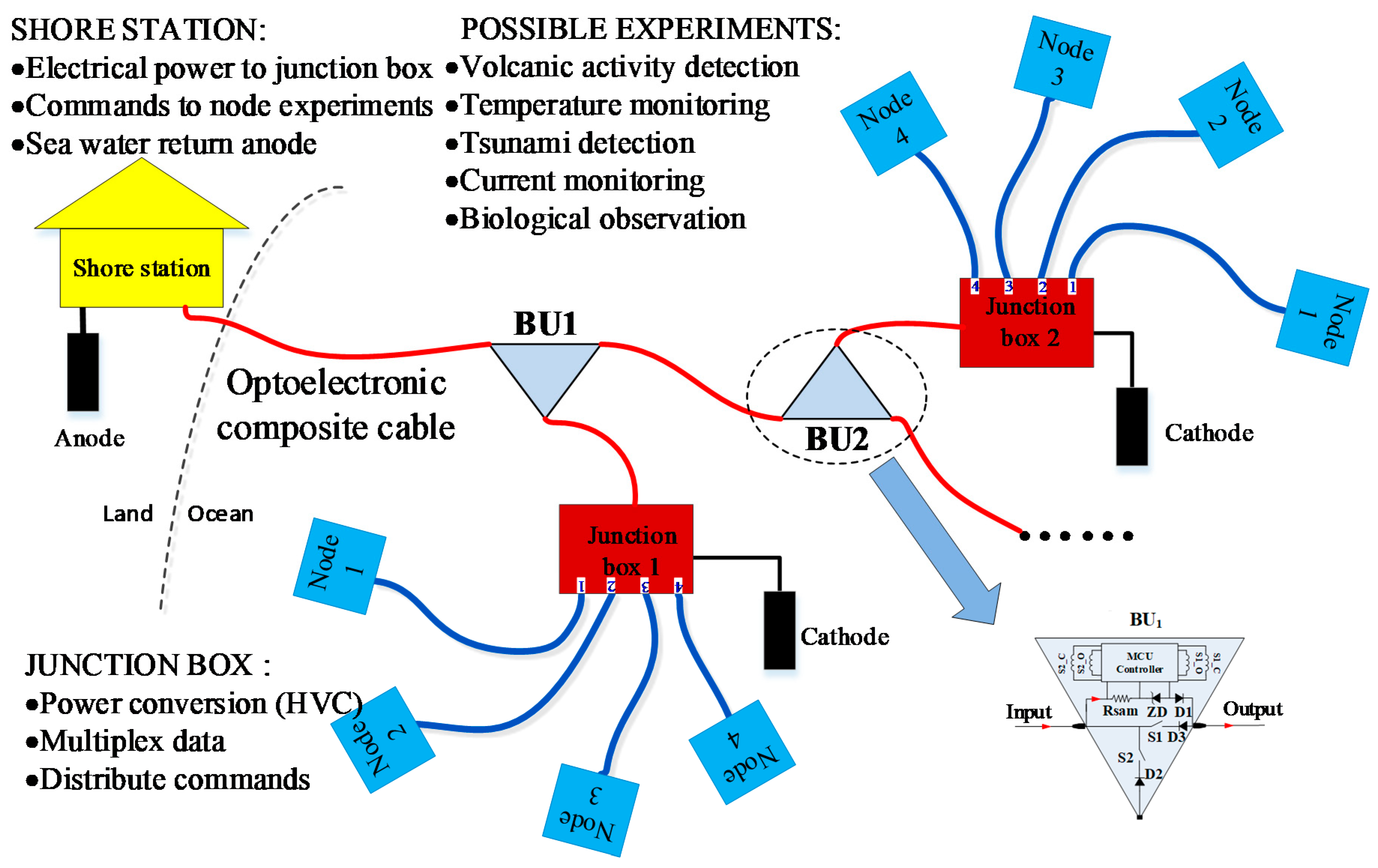
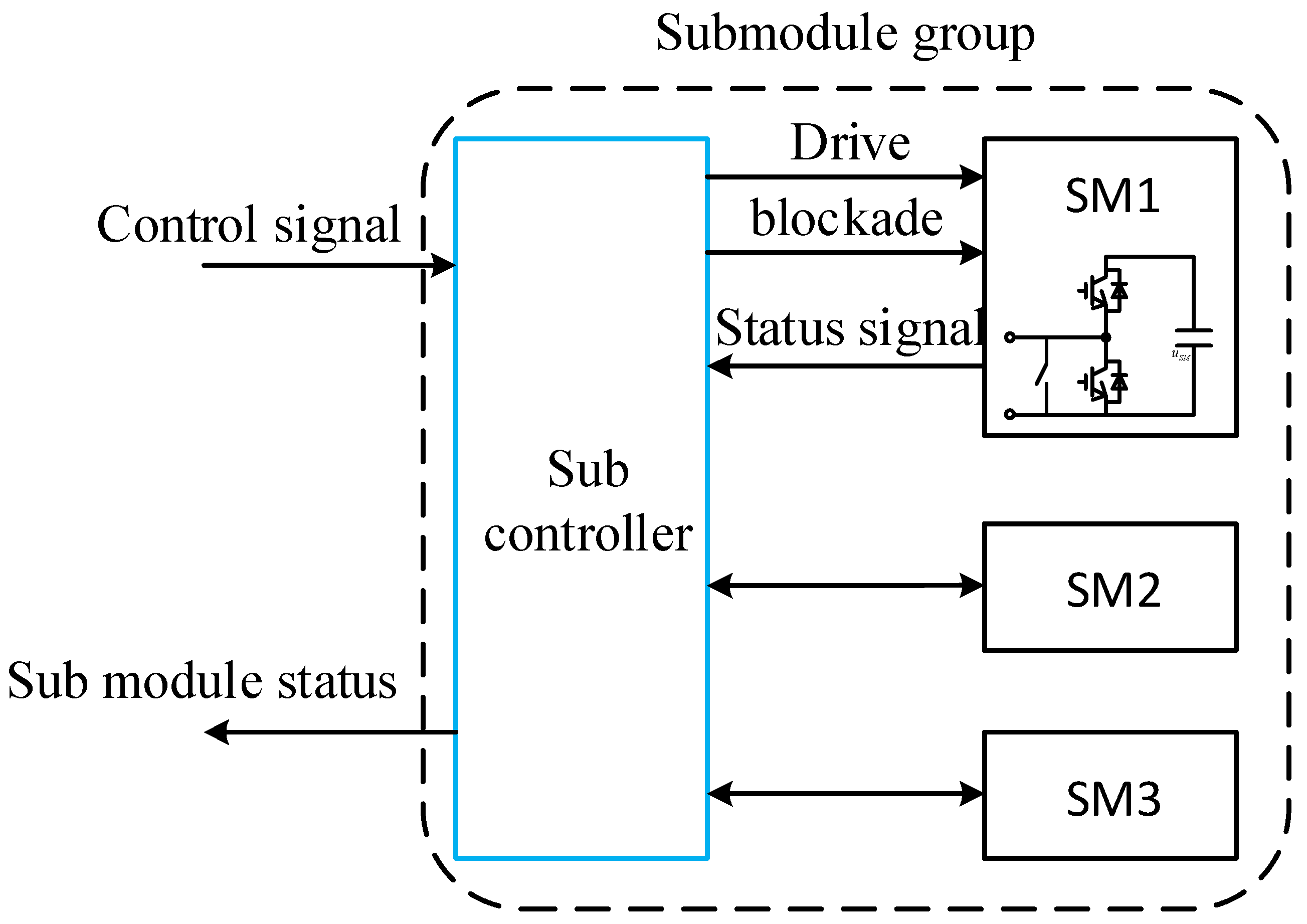
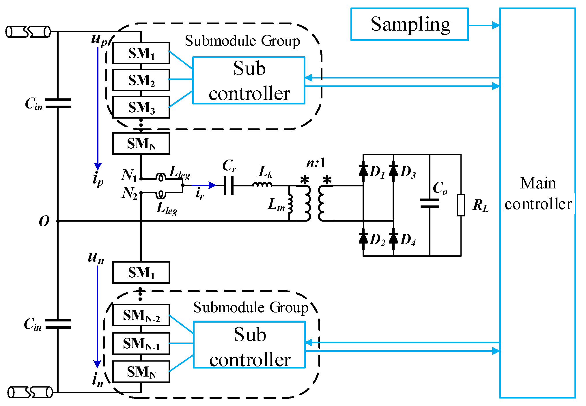
2. System Structure
3. Topology Design of the Main Circuit
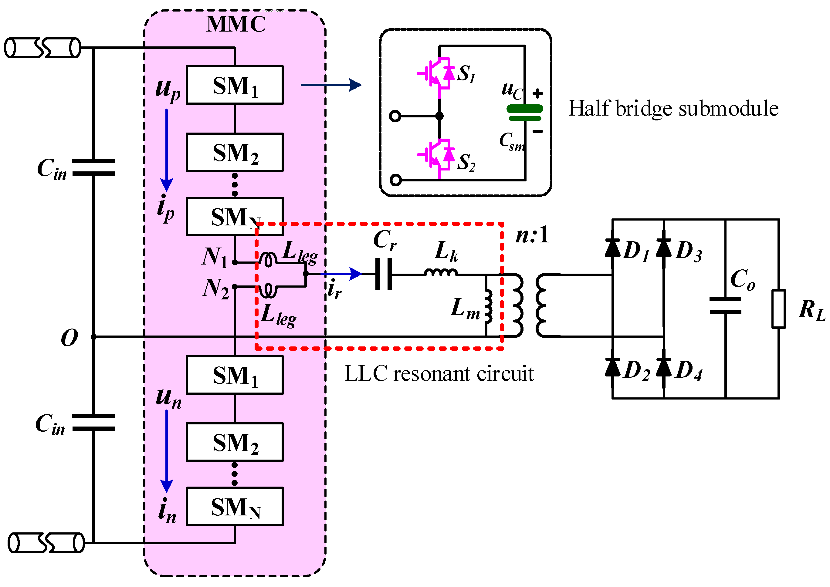
3.1. Topological Structure
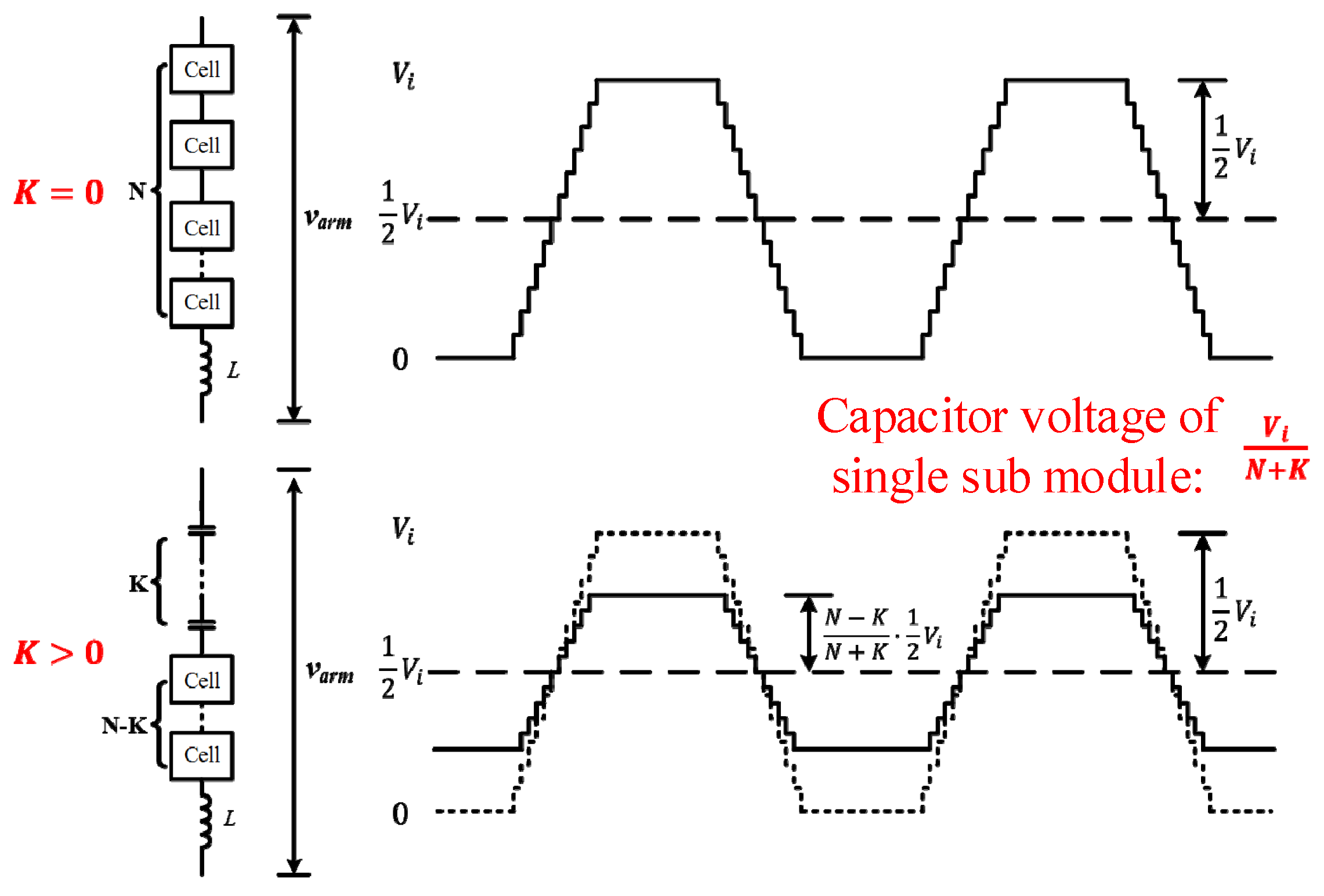
3.2. Voltage Regulation Scheme of Sub-Module Removal
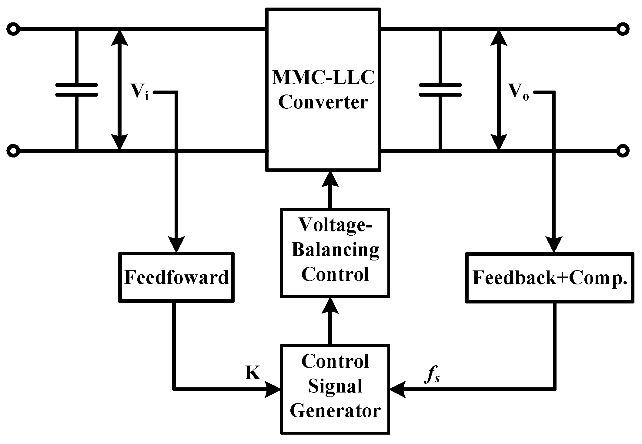
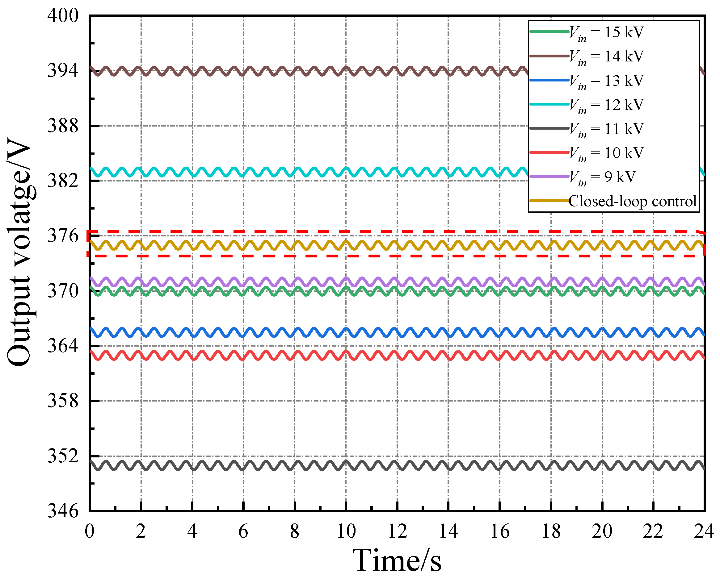
3.3. Closed-Loop Control
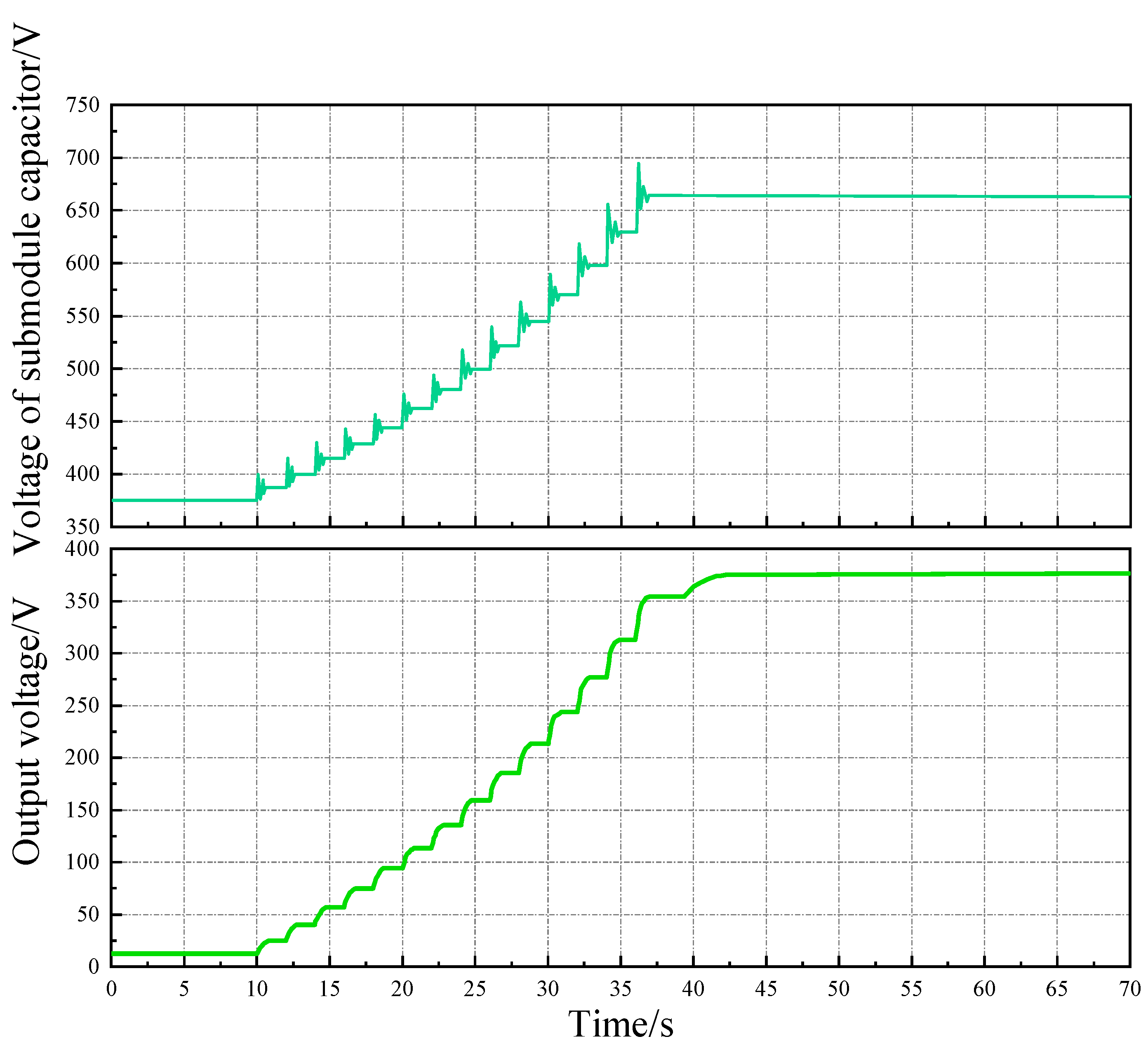
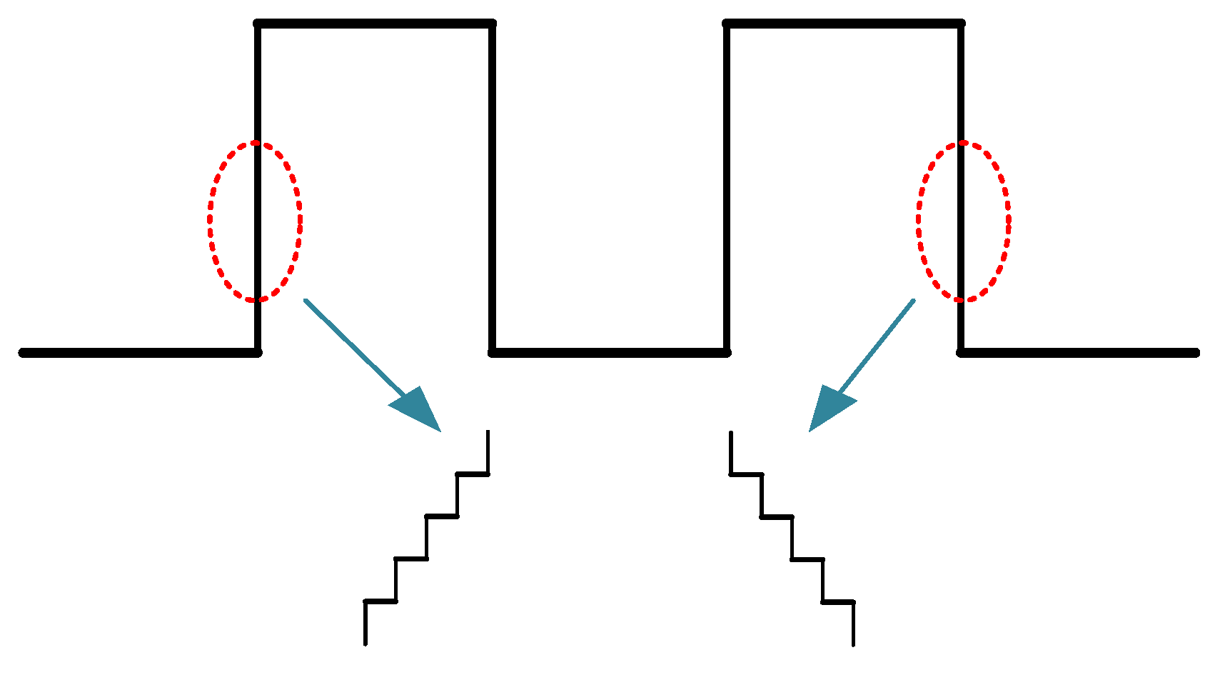
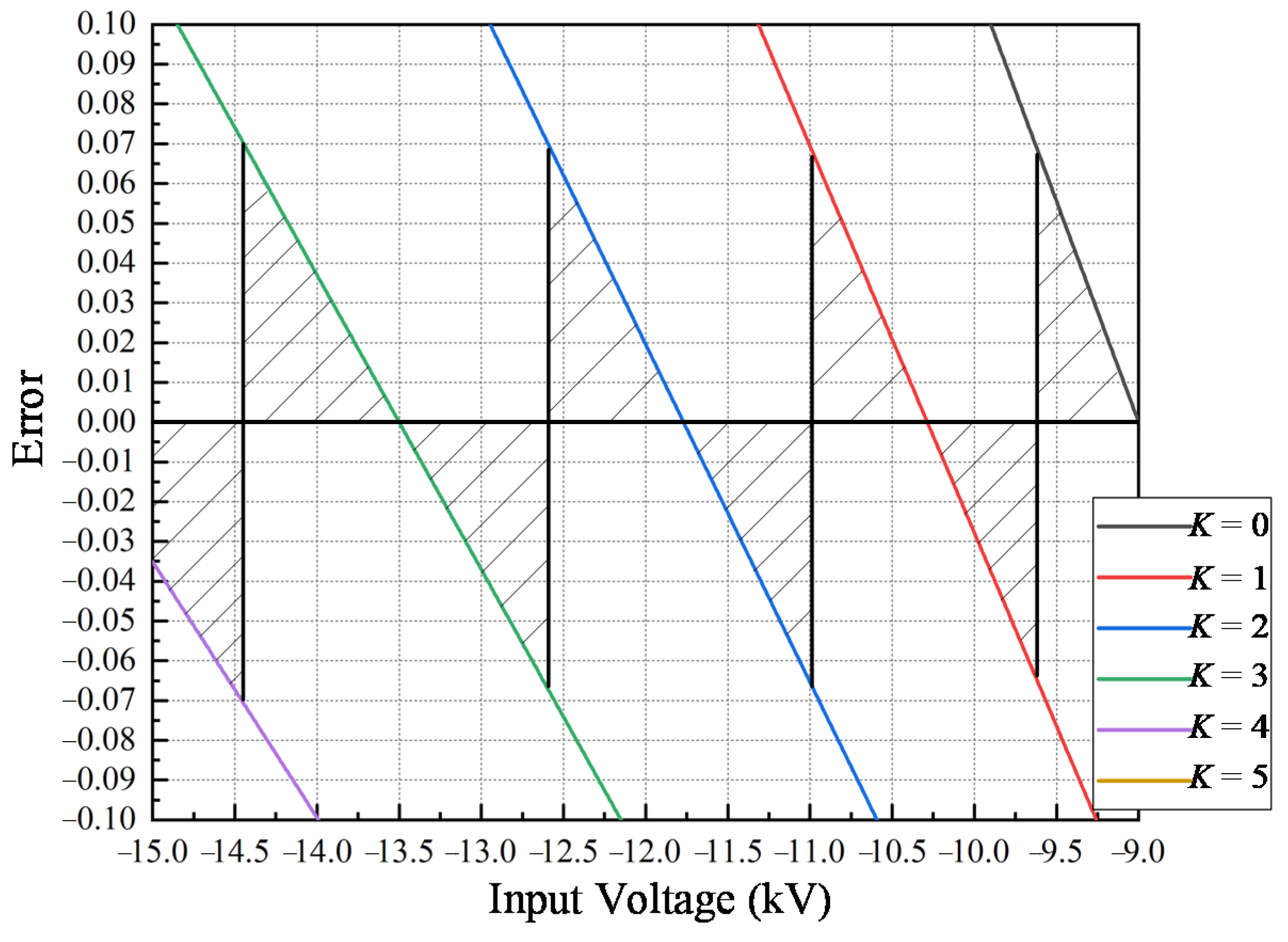
3.4. Error of Sub-Module Voltage Regulation
4. Topological Parameters of the Main Circuit
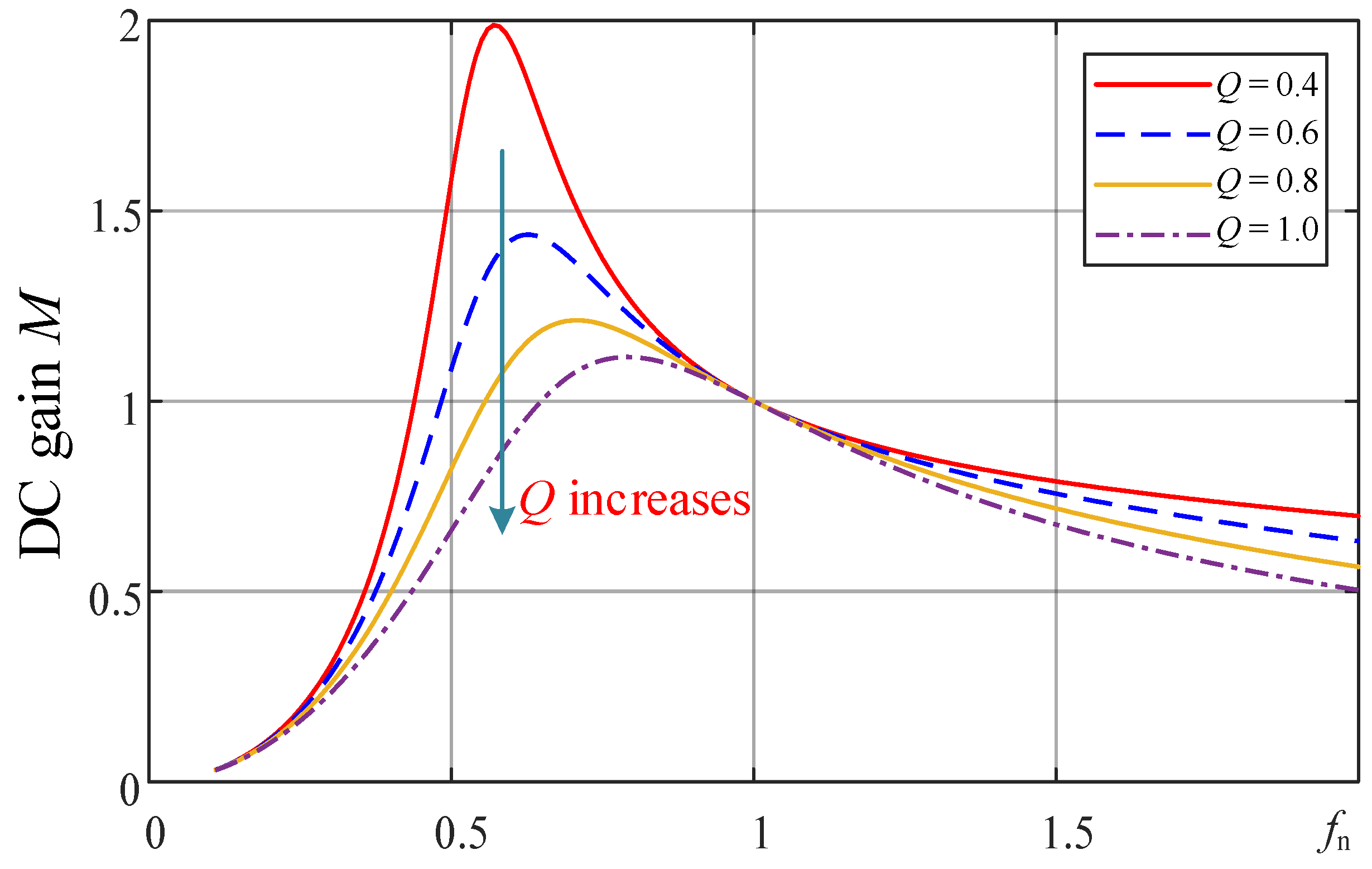
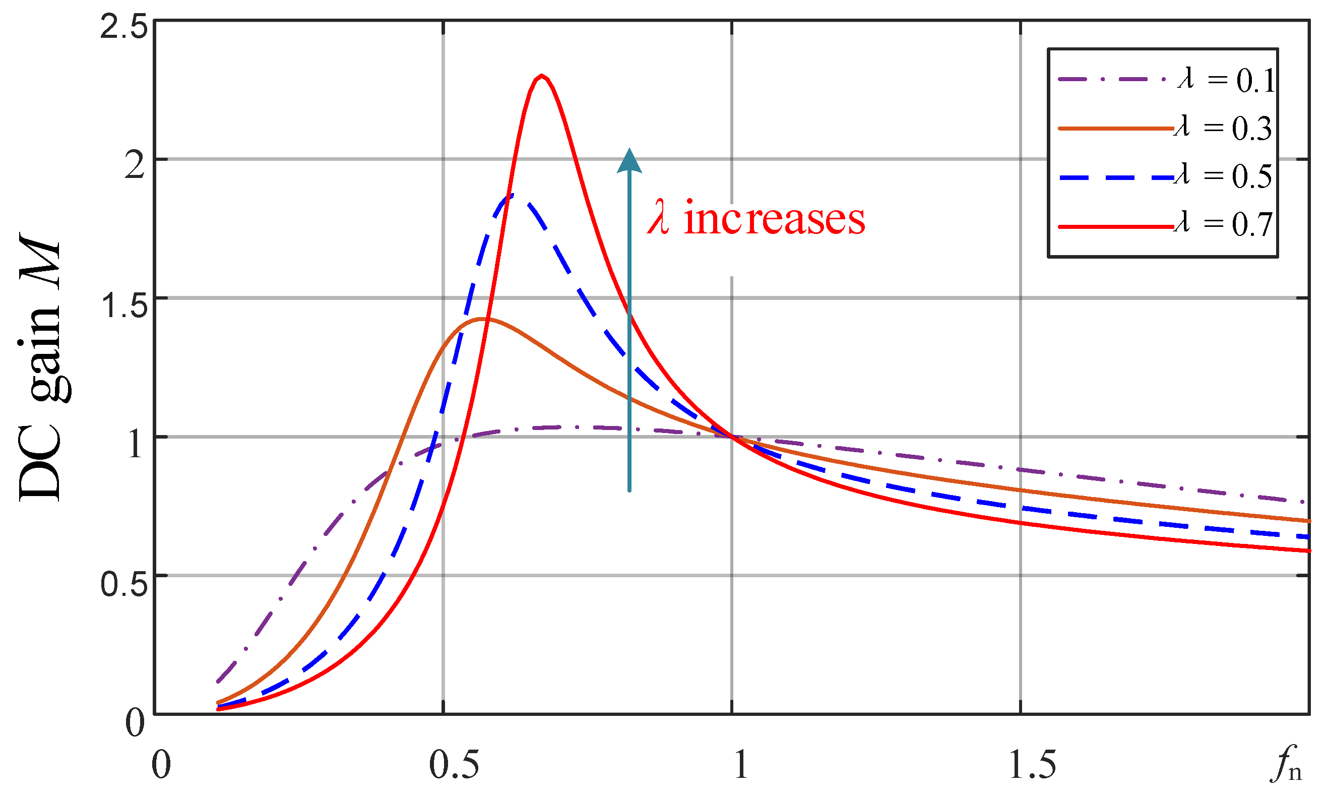
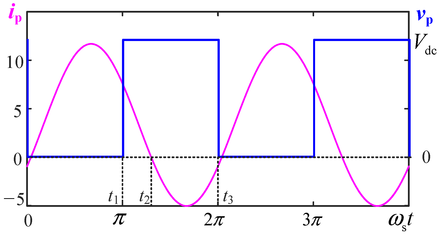
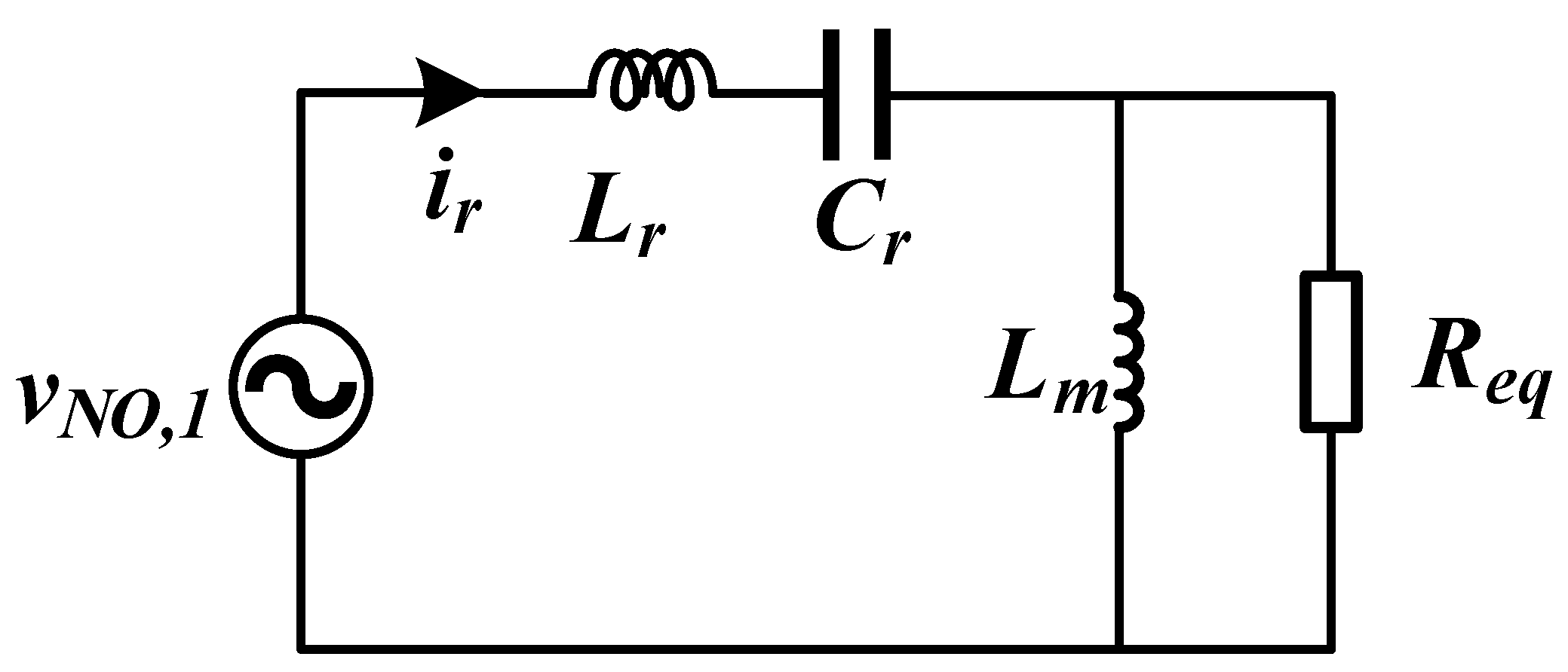
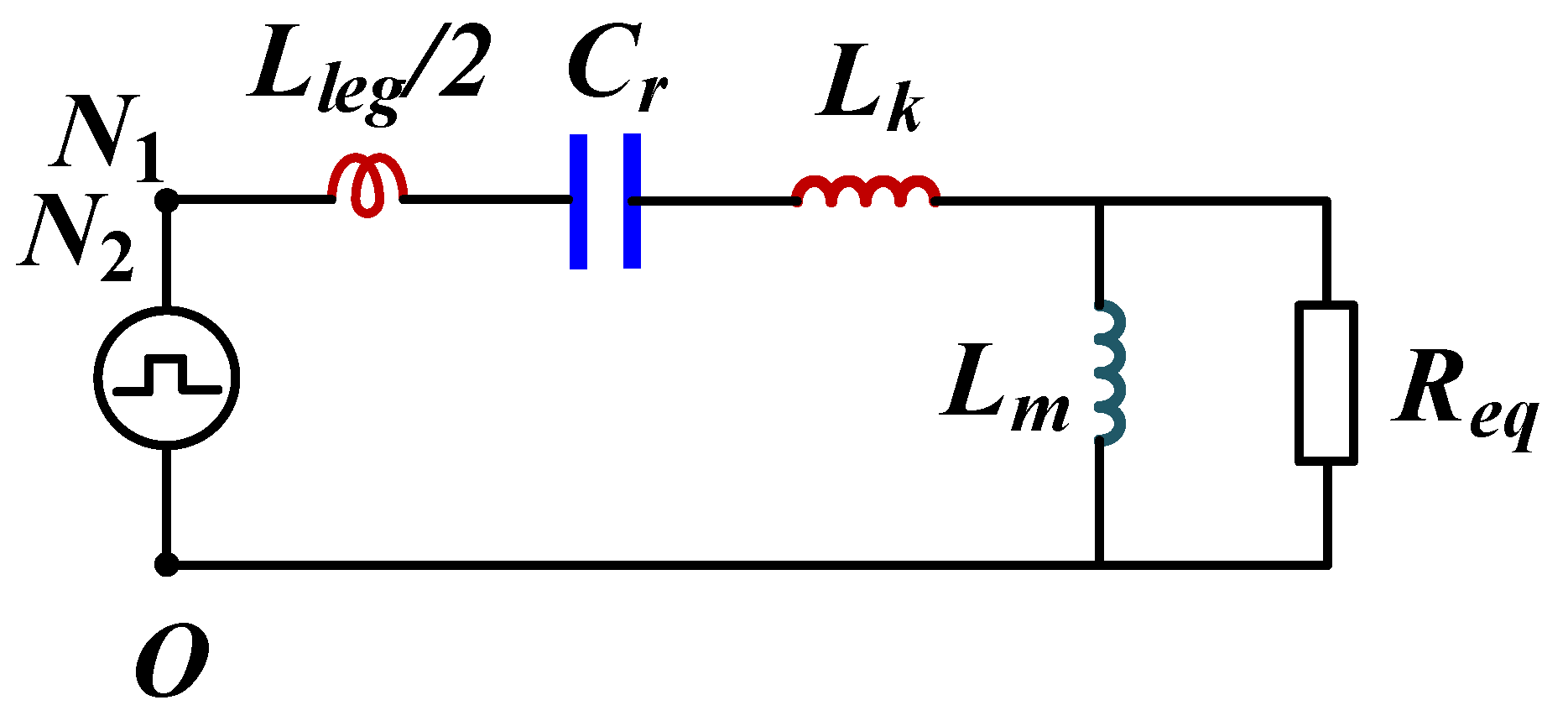
4.1. Resonant Unit
4.2. Modular Unit
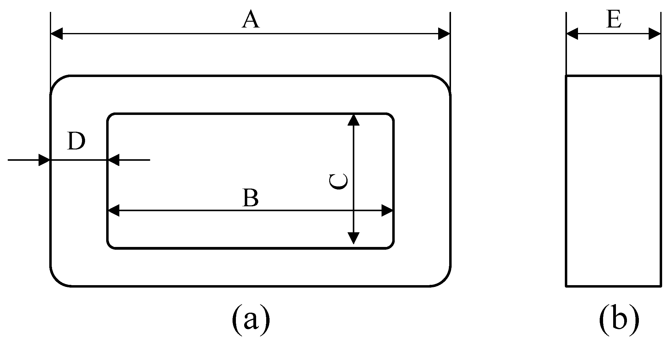
4.3. Transformer
5. Simulation and Laboratory Test
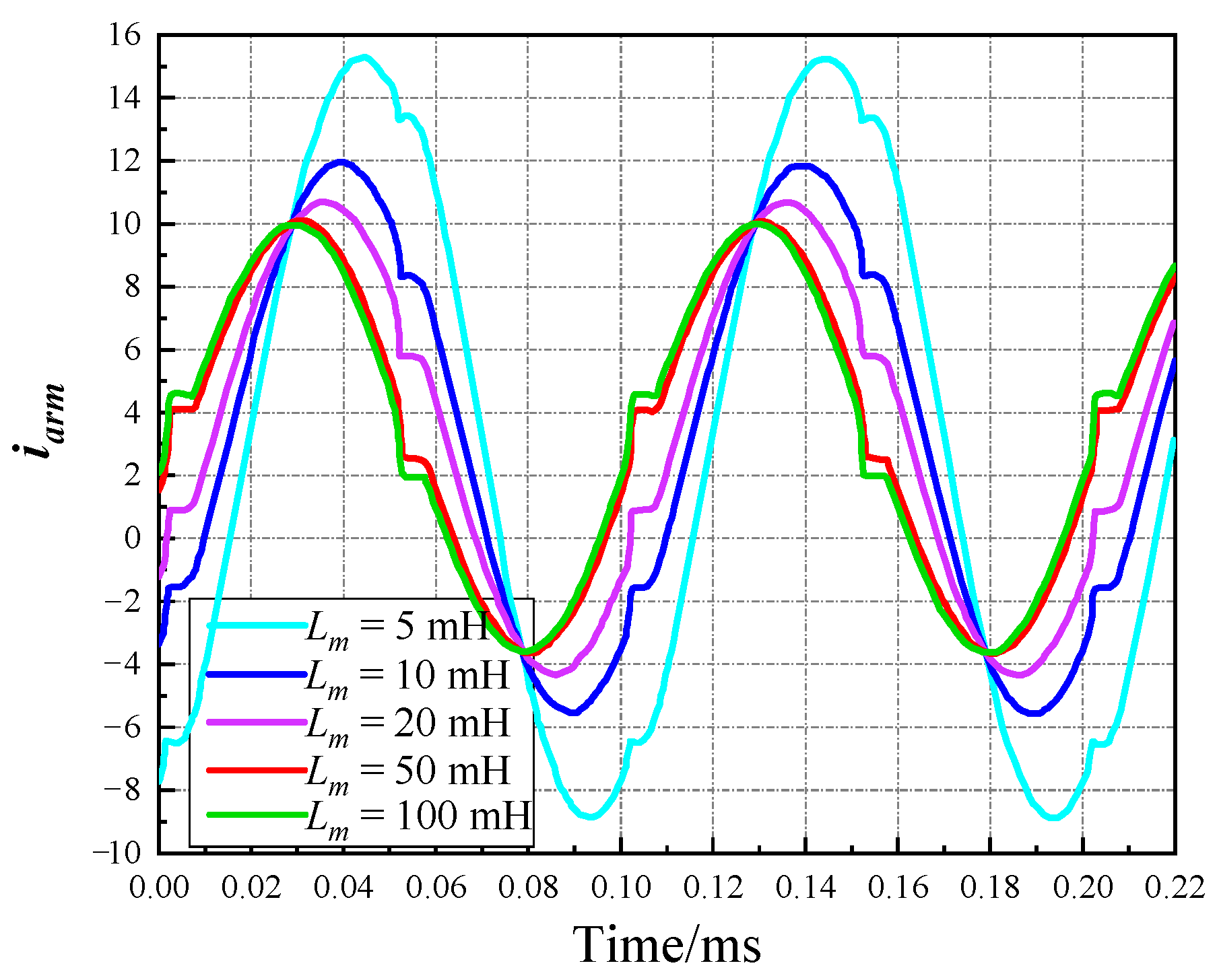
5.1. Simulation Results
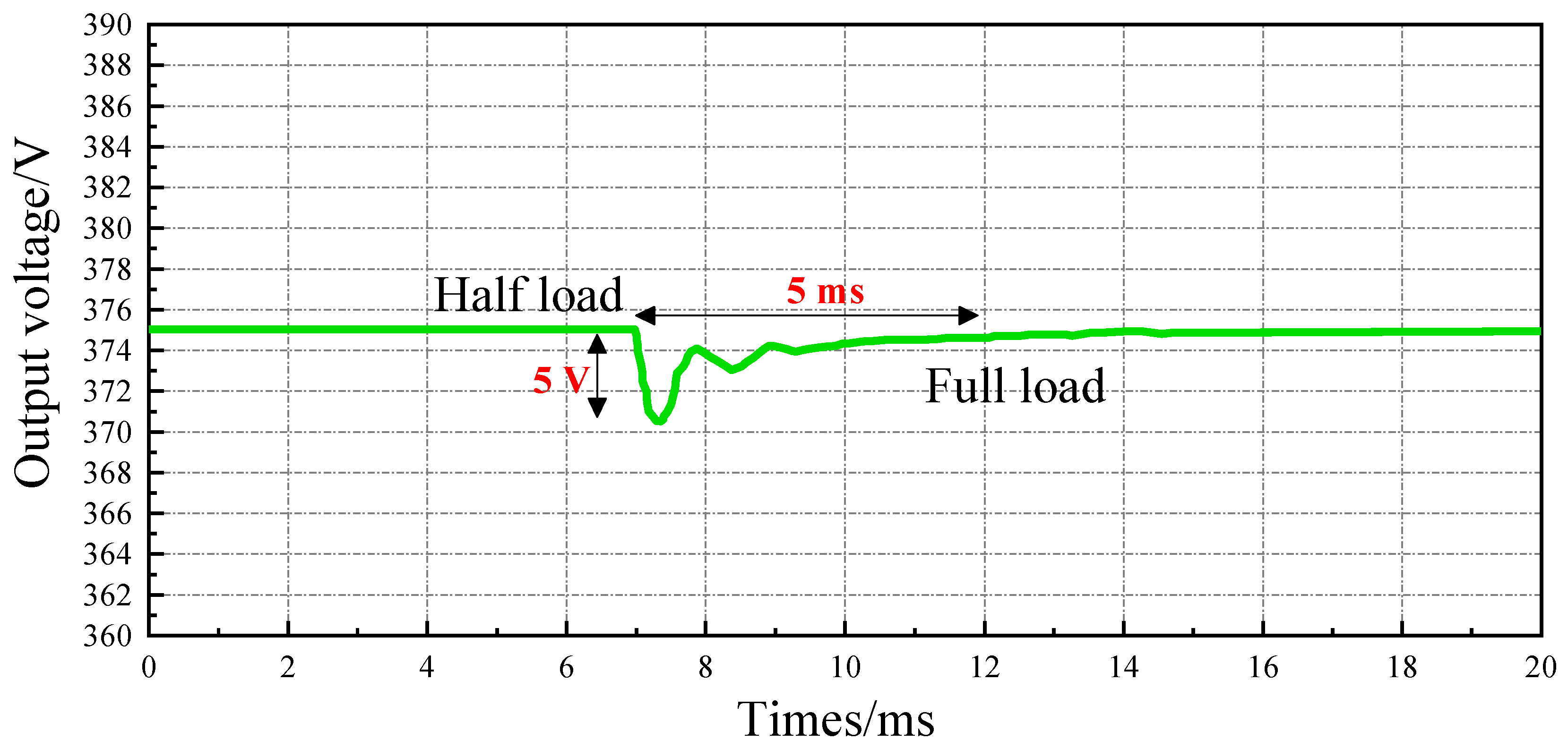
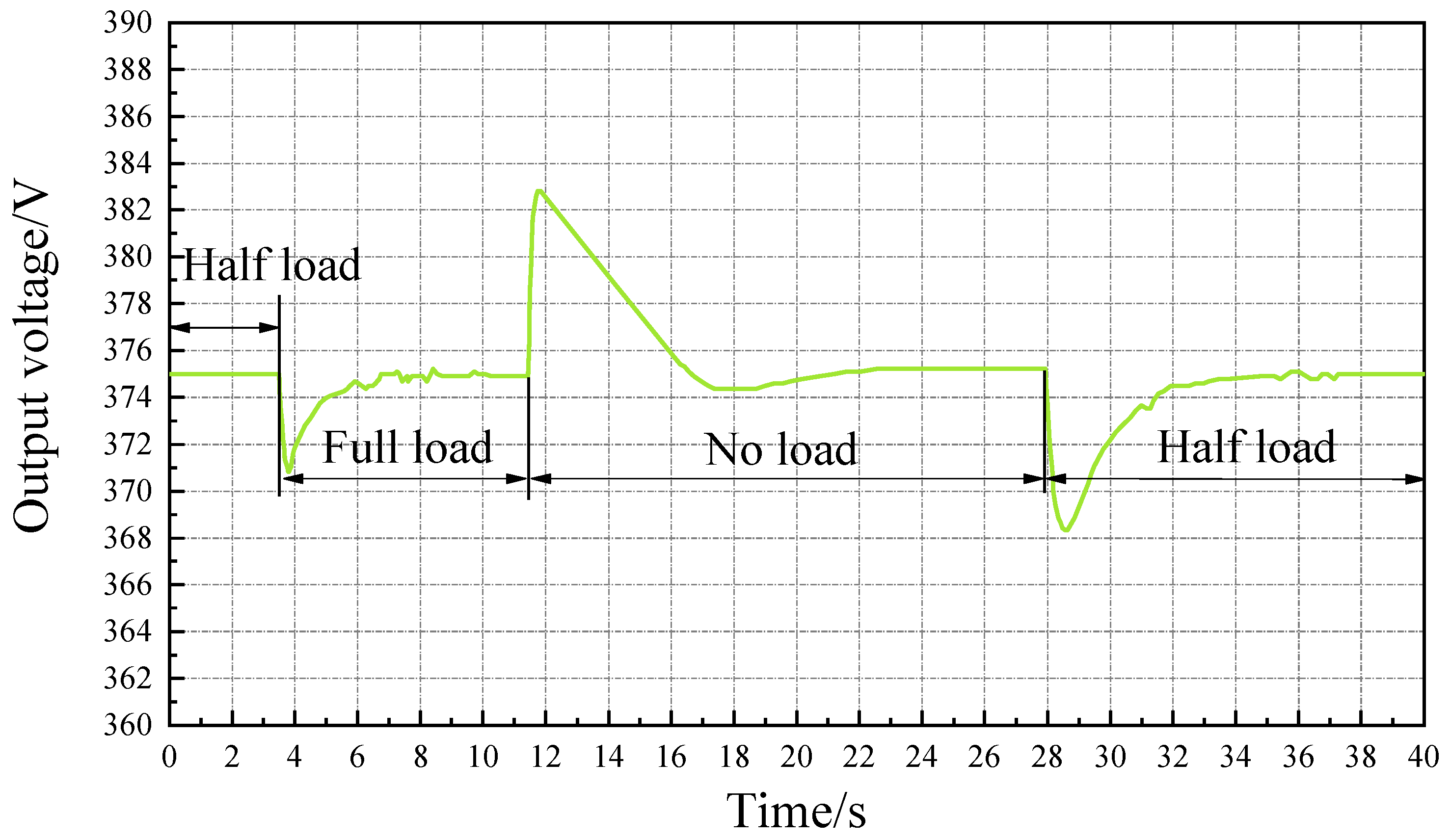
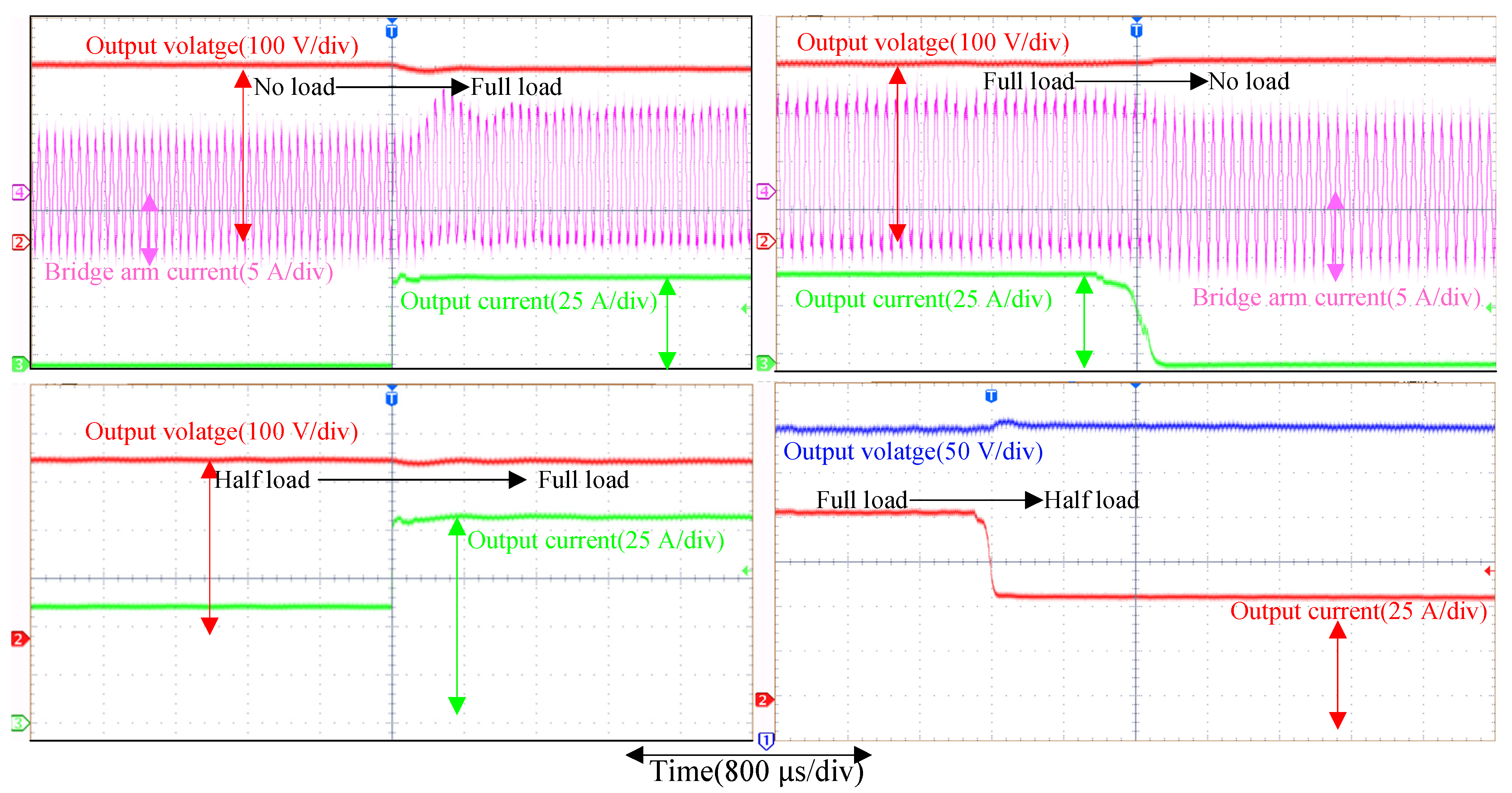
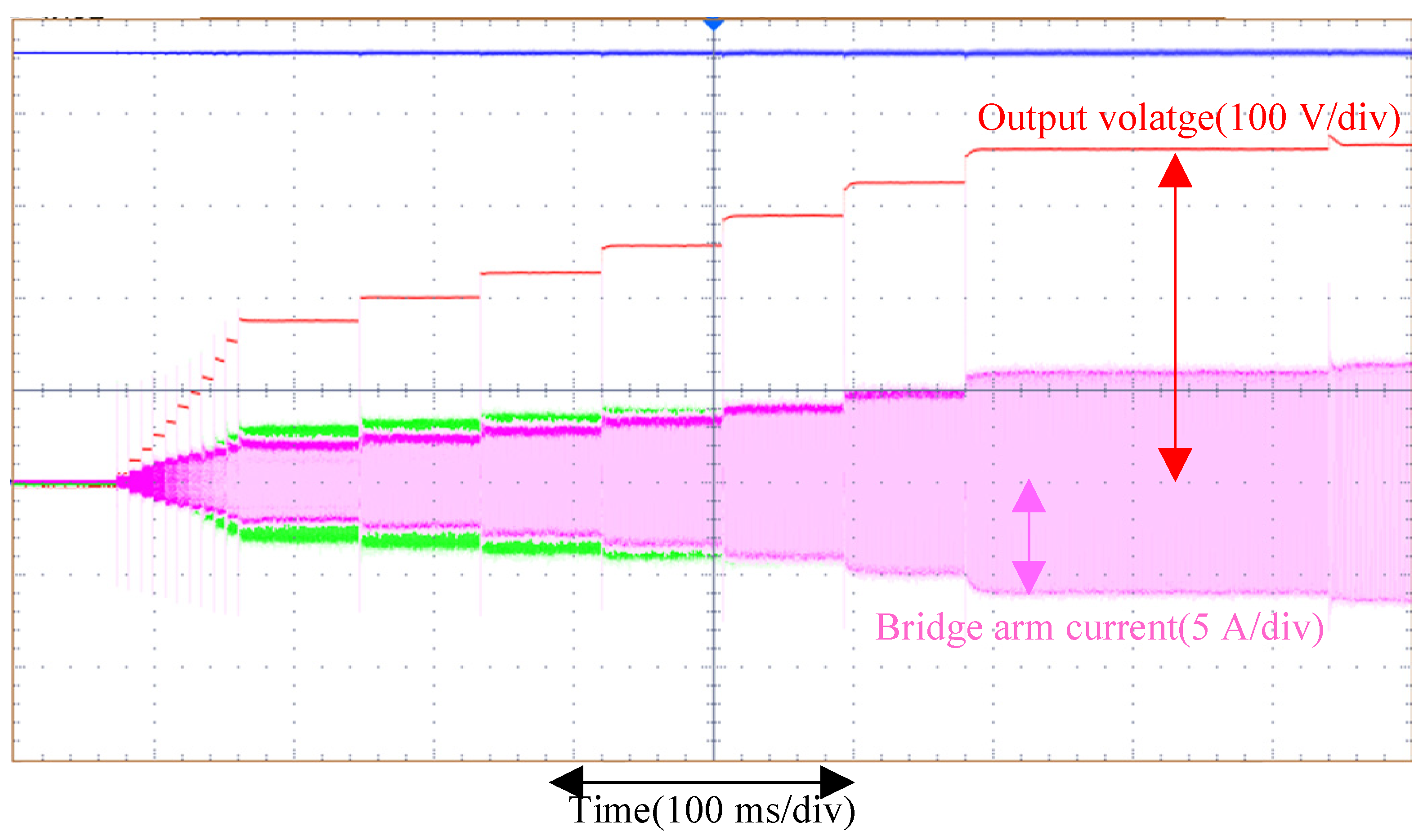
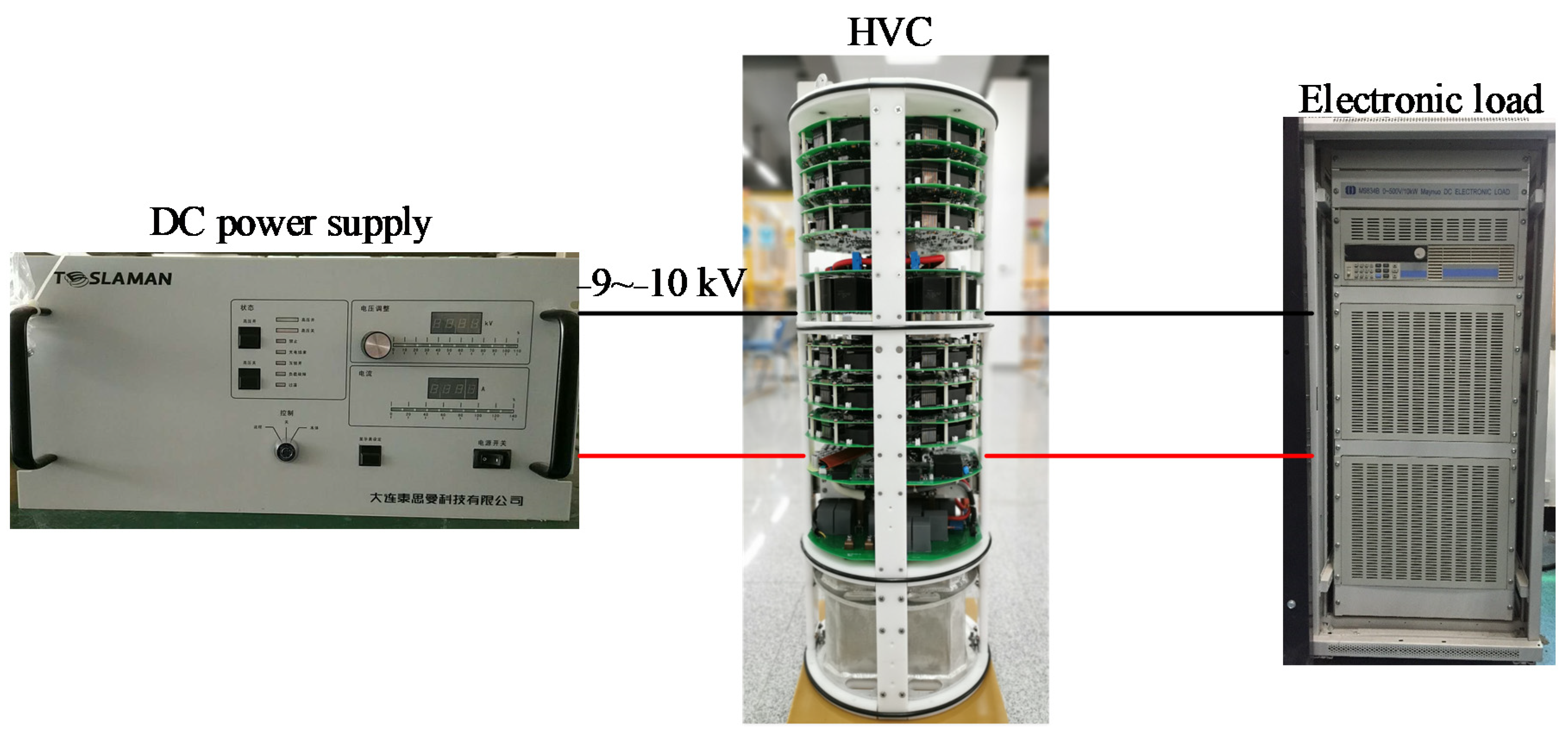
5.2. Experimental Results
6. Conclusions
Author Contributions
Funding
Institutional Review Board Statement
Informed Consent Statement
Data Availability Statement
Conflicts of Interest
References
- Yu, Y.; Xu, H.; Xu, C. A Sensor Web Prototype for Cabled Seafloor Observatories in the East China Sea. J. Mar. Sci. Eng. 2019, 7, 414. [Google Scholar] [CrossRef] [Green Version]
- Yu, J.; Zhang, S.; Yang, W.; Xin, Y.; Gao, H. Design and Application of Buoy Single Point Mooring System with Electro-Optical-Mechanical (EOM) Cable. J. Mar. Sci. Eng. 2020, 8, 672. [Google Scholar] [CrossRef]
- Xiao, S.; Yao, J.; Chen, Y.; Li, D.; Zhang, F.; Wu, Y. Fault Detection and Isolation Methods in Subsea Observation Networks. Sensors 2020, 20, 5273. [Google Scholar] [CrossRef] [PubMed]
- Yu, Y.; Xu, H.; Xu, C. An Object Model for Seafloor Observatory Sensor Control in the East China Sea. J. Mar. Sci. Eng. 2020, 8, 716. [Google Scholar] [CrossRef]
- Von Alt, C.J.; Grassle, J.F. Leo-15 an Unmanned Long Term Environmental Observatory. In Proceedings of the OCEANS’92. Mastering the Oceans through Technology, Newport, RI, USA, 26–29 October 1992; pp. 849–854. [Google Scholar]
- Kawaguchi, K.; Momma, H.; Iwase, R. VENUS project–Submarine cable recovery system. In Proceedings of the 1998 International Symposium on Underwater Technology, Tokyo, Japan, 17 April 1998; pp. 448–452. [Google Scholar]
- Butler, R.; Chave, A.D.; Duennebier, F.K.; Yoerger, D.R.; Petitt, R.; Harris, D.; Wooding, F.B.; Bowen, A.D.; Bailey, J.; Jolly, J.; et al. Hawaii-2 observatory pioneers opportunities for remote instrumentation in ocean studies. Eos Trans. Am. Geophys. Union 2000, 81, 157–163. [Google Scholar] [CrossRef]
- Kasahara, J.; Shirasaki, Y.; Momma, H. Multidisciplinary geophysical measurements on the ocean floor using decommissioned submarine cables: VENUS project. IEEE J. Ocean. Eng. 2000, 25, 111–120. [Google Scholar] [CrossRef]
- Austin, T.; Edson, J.; McGillis, W.; von Alt, C.; Purcell, M.; Petitt, R.; McElroy, M.; Ware, J.; Stokey, R. The Martha’s Vineyard Coastal Observatory: A long term facility for monitoring air-sea processes. In Proceedings of the OCEANS 2000 MTS/IEEE Conference and Exhibition, Providence, RI, USA, 11–14 September 2000; pp. 1937–1941. [Google Scholar]
- Duennebier, F.K.; Harris, D.W.; Jolly, J.; Caplan-Auerbach, J.; Jordan, R.; Copson, D.; Stiffel, K.; Babinec, J.; Bosel, J. HUGO: The Hawaii Undersea Geo-Observatory. IEEE J. Ocean. Eng. 2002, 27, 218–227. [Google Scholar] [CrossRef]
- Henthorn, R.G.; Hobson, B.W.; McGill, P.R.; Sherman, A.D.; Smith, K.L. MARS Benthic Rover: In-situ rapid proto-testing on the Monterey Accelerated Research System. In Proceedings of the OCEANS 2010 MTS/IEEE SEATTLE, Seattle, WA, USA, 20–23 September 2010; pp. 1–7. [Google Scholar]
- Dewey, R.; Tunnicliffe, V. VENUS: Future science on a coastal mid-depth observatory. Scientific Use of Submarine Cables and Related Technologies. In Proceedings of the 2003 International Conference Physics and Control, Tokyo, Japan, 25–27 June 2003; pp. 232–233. [Google Scholar]
- Woodroffe, A.M.; Pridie, S.W.; Druce, G. The NEPTUNE Canada Junction Box: Interfacing science instruments to sub-sea cabled observatories. In Proceedings of the OCEANS 2008-MTS/IEEE Kobe Techno-Ocean, Kobe, Japan, 8–11 April 2008; pp. 1–5. [Google Scholar]
- Yinger, P.; Tennant, P.; Reardon, J.; Harkins, G.; McGuire, C.; Harrington, M.; Mulvihill, M. Commissioning of a system that terminates on the seafloo. In Proceedings of the 2013 OCEANS-San Diego, San Diego, CA, USA, 23–27 September 2013; pp. 1–6. [Google Scholar]
- Delory, E.; Waldmann, C. ESONET, the European Seas Observatory Network. In Proceedings of the World Summit on Ocean Innovations, Kobe, Japan, 8–11 April 2008. [Google Scholar]
- Kawaguchi, K.; Kaneda, Y.; Araki, E. The DONET: A real-time seafloor research infrastructure for the precise earthquake and tsunami monitoring. In Proceedings of the OCEANS 2008-MTS/IEEE Kobe Techno-Ocean, Kobe, Japan, 8–11 April 2008; pp. 121–124. [Google Scholar]
- Kanazawa, T. Japan Trench earthquake and tsunami monitoring network of cable-linked 150 ocean bottom observatories and its impact to earth disaster science. In Proceedings of the 2013 IEEE International Underwater Technology Symposium (UT), Tokyo, Japan, 5–8 March 2013; pp. 1–5. [Google Scholar]
- Chen, Y.H.; Yang, C.J.; Li, D.J.; Jin, B.; Chen, Y. Study on 10 kVDC powered junction box for a cabled ocean observatory system. China Ocean Eng. 2013, 27, 265–275. [Google Scholar] [CrossRef]
- Chen, Y.; Xiao, S.; Li, D. Stability Analysis Model for Multi-Node Undersea Observation Networks. Simul. Model. Pract. Theory 2019, 97, 101971. [Google Scholar] [CrossRef]
- Yang, F.; Lyu, F. A Novel Fault Location Approach for Scientific Cabled Seafloor Observatories. J. Mar. Sci. Eng. 2020, 8, 190. [Google Scholar] [CrossRef] [Green Version]
- Dekka, A.; Wu, B.; Fuentes, R.L.; Perez, M.; Zargari, N.R. Evolution of Topologies, Modeling, Control Schemes, and Applications of Modular Multilevel Converters. IEEE J. Emerg. Sel. Top. Power Electron. 2017, 5, 1631–1656. [Google Scholar] [CrossRef]
- Kenzelmann, S.; Rufer, A.; Dujic, D.; Canales, F.; De Novaes, Y.R. Isolated DC/DC Structure Based on Modular Multilevel Converter. IEEE Trans. Power Electron. 2015, 30, 89–98. [Google Scholar] [CrossRef]
- Zhang, J.; Wang, Z.; Shao, S.A. Three-Phase Modular Multilevel DC–DC Converter for Power Electronic Transformer Applications. IEEE J. Emerg. Sel. Top. Power Electron. 2017, 5, 140–150. [Google Scholar] [CrossRef]


| Transformer | Maximum Flux/T | Current Density | Efficiency/% | Size/mm (Length ∗ Width ∗ Height) | Volume/L |
|---|---|---|---|---|---|
| 60 kVA/10 kHz | 0.302 | 4.04 | 99.6 | 225 ∗ 225 ∗ 127 | 6.429375 |
| Electronic Component | Value | Electronic Component | Value |
|---|---|---|---|
| DC input voltage Vdc | −9 kV~−15 kV | Bridge arm inductance Lleg | 688.6 μH |
| DC output voltage | 375 V | Leakage inductance of transformer Lk | 844.3 μH |
| Output power Po | 40 kW | Resonant capacitor Cr | 300 nF |
| Number of sub-modules of single bridge arm N | 15 + 3 | Excitation inductance of transformer Lm | 10 mH |
| Capacitance of sub-module Csm | 10 uF | Closed-loop frequency modulation range fs | 8 kHz~12 kHz |
| Rated voltage of sub-module Vsm | 655 V | DC input capacitance Cin | 10 μF |
| resonant frequency fr | 10k Hz | DC output filter capacitor Co | 600 μF |
Publisher’s Note: MDPI stays neutral with regard to jurisdictional claims in published maps and institutional affiliations. |
© 2021 by the authors. Licensee MDPI, Basel, Switzerland. This article is an open access article distributed under the terms and conditions of the Creative Commons Attribution (CC BY) license (https://creativecommons.org/licenses/by/4.0/).
Share and Cite
Zhang, F.; Zhang, Z.; Xiao, S.; Xie, K.; Ni, J.; Gu, H.; Wu, Y.; Ning, Y.; Xia, Q. Design and Implementation for the High Voltage DC-DC Converter of the Subsea Observation Network. J. Mar. Sci. Eng. 2021, 9, 712. https://doi.org/10.3390/jmse9070712
Zhang F, Zhang Z, Xiao S, Xie K, Ni J, Gu H, Wu Y, Ning Y, Xia Q. Design and Implementation for the High Voltage DC-DC Converter of the Subsea Observation Network. Journal of Marine Science and Engineering. 2021; 9(7):712. https://doi.org/10.3390/jmse9070712
Chicago/Turabian StyleZhang, Feng, Zhifeng Zhang, Sa Xiao, Kai Xie, Jiawei Ni, Haolun Gu, Yong Wu, Yang Ning, and Qingchao Xia. 2021. "Design and Implementation for the High Voltage DC-DC Converter of the Subsea Observation Network" Journal of Marine Science and Engineering 9, no. 7: 712. https://doi.org/10.3390/jmse9070712
APA StyleZhang, F., Zhang, Z., Xiao, S., Xie, K., Ni, J., Gu, H., Wu, Y., Ning, Y., & Xia, Q. (2021). Design and Implementation for the High Voltage DC-DC Converter of the Subsea Observation Network. Journal of Marine Science and Engineering, 9(7), 712. https://doi.org/10.3390/jmse9070712