
Normally-Off p-GaN Gated AlGaN/GaN MIS-HEMTs with ALD-Grown Al2O3/AlN Composite Gate Insulator

 ,
,  ,
, 
Abstract
:1. Introduction
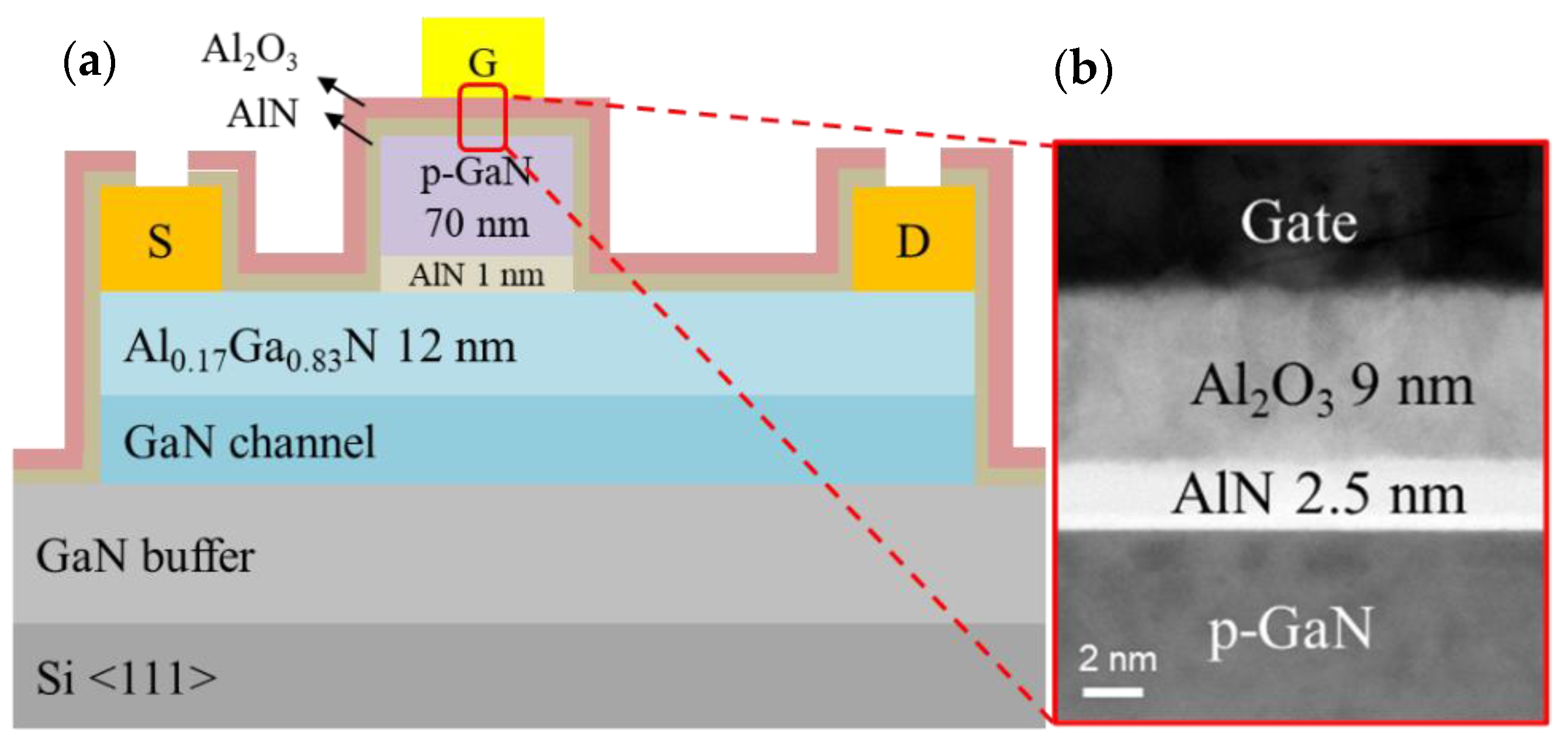
2. Device Structure
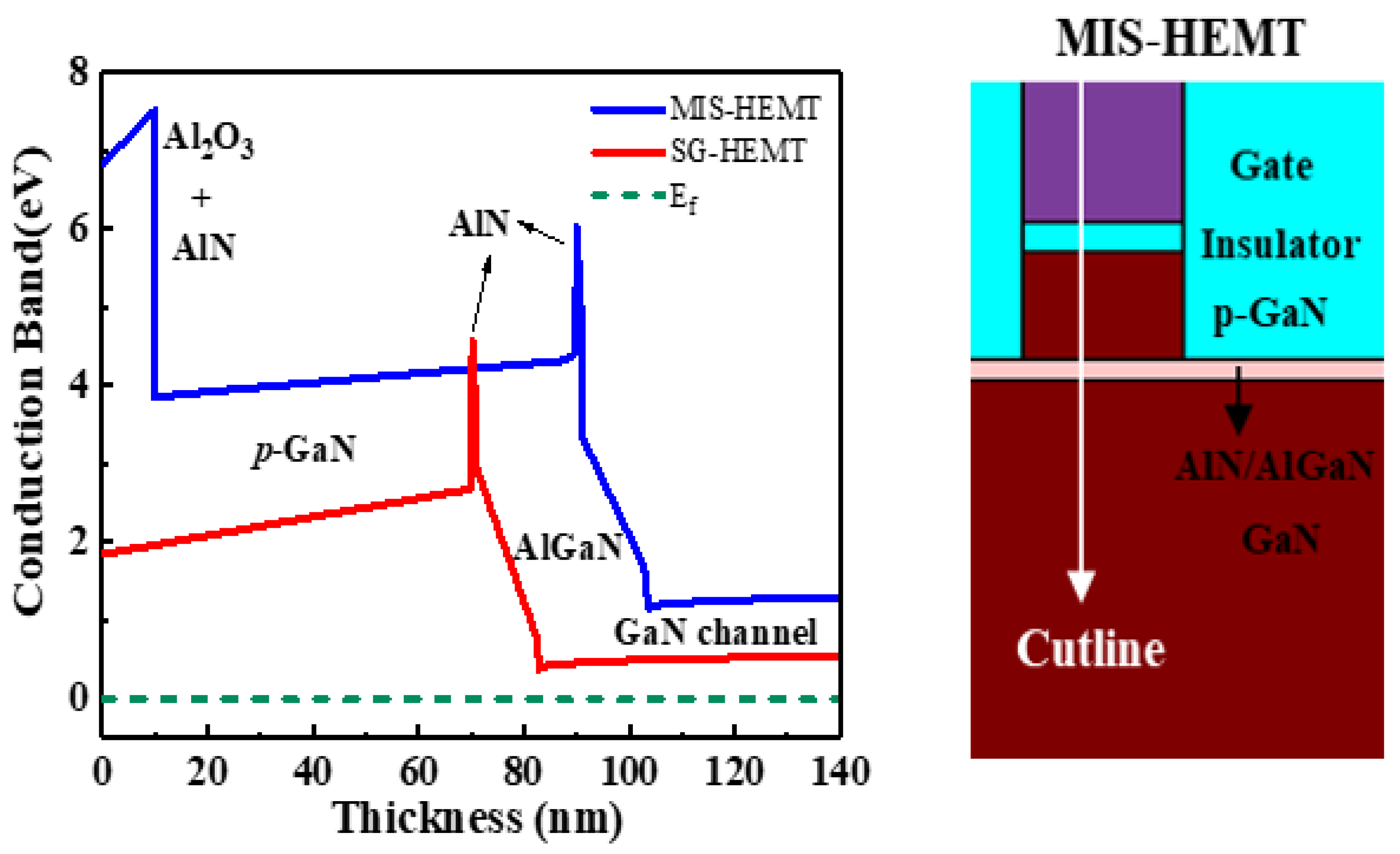
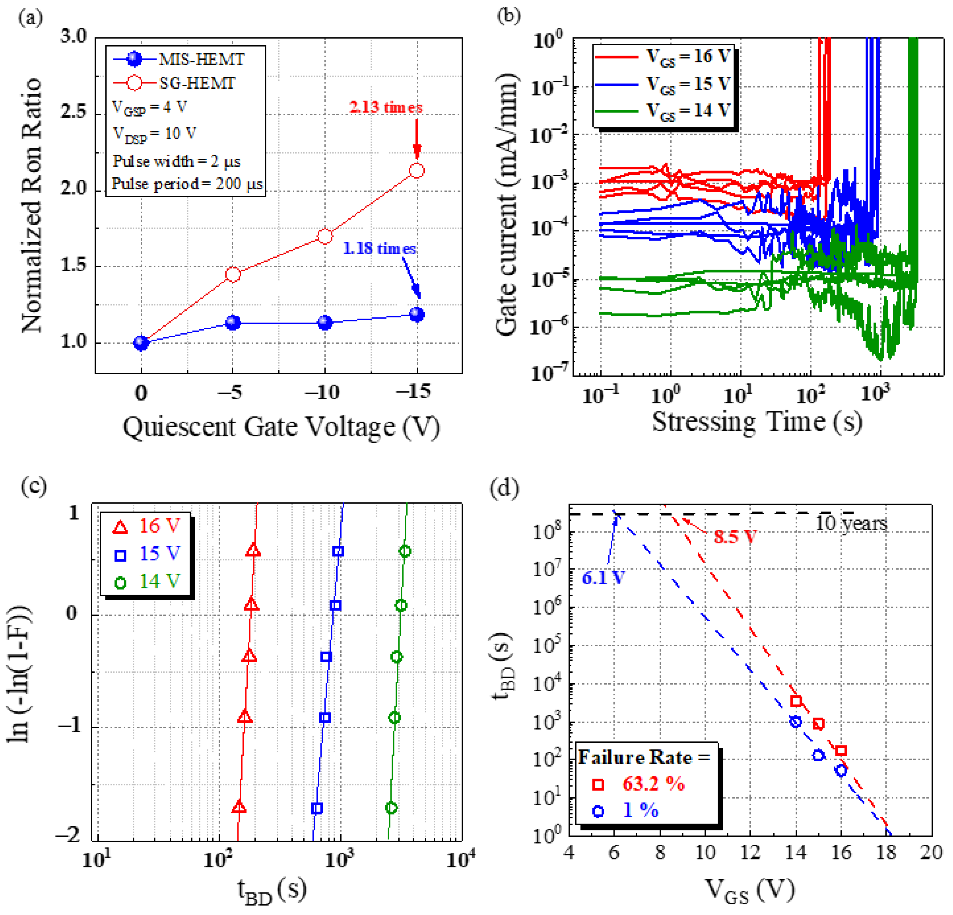
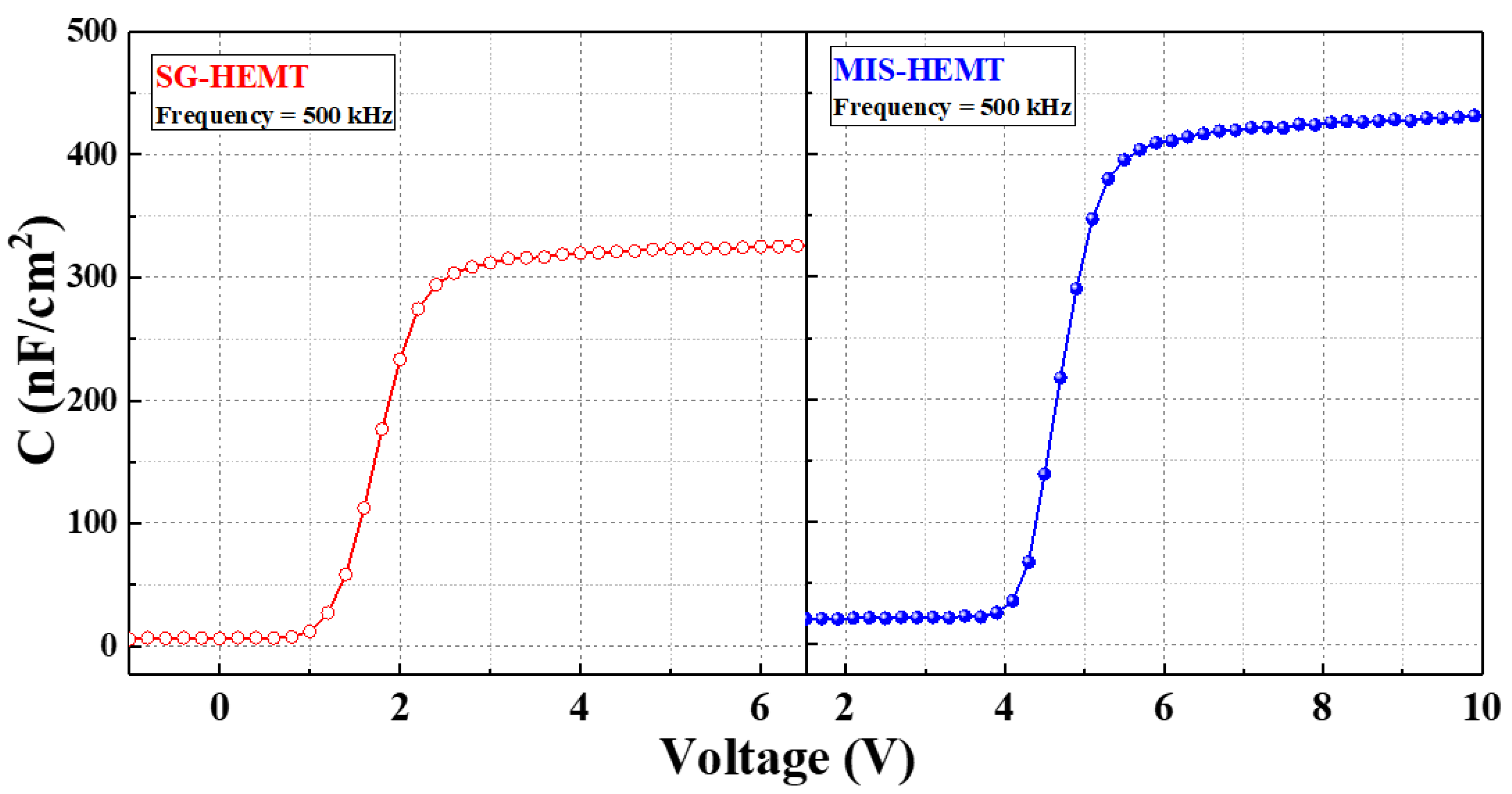
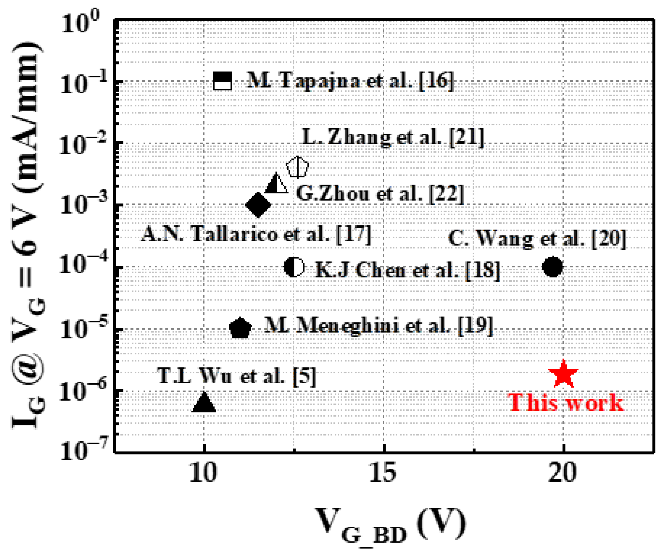
3. Experimental Result and Discussion
4. Conclusions
Author Contributions
Funding
Institutional Review Board Statement
Informed Consent Statement
Conflicts of Interest
References
- Saito, W.; Takada, Y.; Kuraguchi, M.; Tsuda, K.; Omura, I.; Ogura, T.; Ohashi, H. High breakdown voltage AlGaN-GaN power-HEMT design and high current density switching behavior. IEEE Trans. Electron Devices 2003, 50, 2528–2531. [Google Scholar] [CrossRef]
- Cai, Y.; Zhou, Y.; Chen, K.J.; Lau, K.M. High-performance enhancement-mode AlGaN/GaN HEMTs using fluoride-based plasma treatment. IEEE Electron Device Lett. 2005, 26, 435–437. [Google Scholar] [CrossRef]
- Palacios, T.; Suh, C.; Chakraborty, A.; Keller, S.; DenBaars, S.P.; Mishra, U.K. High-performance E-mode AlGaN/GaN HEMTs. IEEE Electron Device Lett. 2006, 27, 428–430. [Google Scholar] [CrossRef]
- Hwang, I.; Oh, J.; Choi, H.S.; Kim, J.; Choi, H.; Kim, J.; Chong, S.; Shin, J.; Chung, U.I. Source-Connected p-GaN Gate HEMTs for Increased Threshold Voltage. IEEE Electron Device Lett. 2013, 34, 605–607. [Google Scholar] [CrossRef]
- Wu, T.-L.; Marcon, D.; You, S.; Posthuma, N.; Bakeroot, B.; Stoffels, S.; Van Hove, M.; Groeseneken, G.; Decoutere, S. Forward Bias Gate Breakdown Mechanism in Enhancement-Mode p-GaN Gate AlGaN/GaN High-Electron Mobility Transistors. IEEE Electron Device Lett. 2015, 36, 1001–1003. [Google Scholar] [CrossRef]
- Chiu, H.-C.; Chang, Y.-S.; Li, B.-H.; Wang, H.-C.; Kao, H.-L.; Chien, F.-T.; Hu, C.-W.; Xuan, R. High Uniformity Normally-OFF p-GaN Gate HEMT Using Self-Terminated Digital Etching Technique. IEEE Trans. Electron Devices 2018, 65, 4820–4825. [Google Scholar] [CrossRef]
- Liu, X.; Chiu, H.-C.; Liu, C.-H.; Kao, H.-L.; Chiu, C.-W.; Wang, H.-C.; Ben, J.; He, W.; Huang, C.-R. Normally-off p-GaN Gated AlGaN/GaN HEMTs Using Plasma Oxidation Technique in Access Region. IEEE J. Electron Devices Soc. 2020, 8, 229–234. [Google Scholar] [CrossRef]
- Hao, R.; Xu, N.; Yu, G.; Song, L.; Chen, F.; Zhao, J.; Deng, X.; Li, X.; Cheng, K.; Fu, K.; et al. Studies on fabrication and reliability of GaN highresistivity- cap-layer HEMT. IEEE Trans. Electron Devices 2018, 65, 1314–1320. [Google Scholar] [CrossRef]
- Tajalli, A. Impact of sidewall etching on the dynamic performance of GaN-on-Si E-mode transistors. Microelectron. Reliab. 2018, 88–90, 572–576. [Google Scholar] [CrossRef]
- Hao, R.; Li, W.; Fu, K.; Yu, G.; Song, L.; Yuan, J.; Li, J.; Deng, X.; Zhang, X.; Zhou, Q.; et al. Breakdown Enhancement and Current Collapse Suppression by High-Resistivity GaN Cap Layer in Normally-Off AlGaN/GaN HEMTs. IEEE Electron Device Lett. 2017, 38, 1567–1570. [Google Scholar] [CrossRef]
- Takhar, K. Al2O3 formed by post plasma oxidation of Al as a Gate dielectric for AlGaN/GaN MIS-HEMTs. Appl. Surf. Sci. 2019, 481, 219–225. [Google Scholar] [CrossRef]
- Buttari, D.; Chini, A.; Chakraborty, A.; Mccarthy, L.; Xing, H.; Palacios, T.; Shen, L.; Keller, S.; Mishra, U.K. Selective dry etching of GaN over AlGaN in BCl3/SF6 mixtures. Proc. IEEE Lester Eastman Conf. High Perform. Devices 2004, 14, 756–761. [Google Scholar] [CrossRef]
- Pu, T.; Wang, X.; Huang, Q.; Zhang, T.; Li, X.; Li, L.; Ao, J.-P. Normally-Off AlGaN/GaN Heterojunction Metal-Insulator-Semiconductor Field-Effect Transistors with Gate-First Process. IEEE Electron Device Lett. 2019, 40, 185–188. [Google Scholar] [CrossRef]
- Chen, K.J. AlN passivation by plasma-enhanced atomic layer deposition for GaN-based power switches and power amplifiers. Semicond. Sci. Technol. 2013, 28, 074015. [Google Scholar] [CrossRef]
- Degraeve, R. Degradation and breakdown in thin oxide layers: Mechanisms, models and reliability prediction. Microelectron. Reliab. 1999, 39, 1445–1460. [Google Scholar] [CrossRef]
- Ťapajna, M.; Hilt, O.; Bahat-Treidel, E.; Würfl, J.; Kuzmík, J. Gate Reliability Investigation in Normally-Off p-Type-GaN Cap/AlGaN/GaN HEMTs Under Forward Bias Stress. IEEE Electron Device Lett. 2016, 37, 385–388. [Google Scholar] [CrossRef]
- Tallarico, A.N. Perimeter driven transport in the p-GaN gate as a limiting factor for gate reliability. Proc. IEEE Int. Rel. Phys. Symp. (IRPS) 2019, 1–10. [Google Scholar] [CrossRef]
- He, J.; Wei, J.; Yang, S.; Wang, Y.; Zhong, K.; Chen, K.J. Frequency- and Temperature-Dependent Gate Reliability of Schottky-Type p-GaN Gate HEMTs. IEEE Trans. Electron Devices 2019, 66, 3453–3458. [Google Scholar] [CrossRef]
- Stockman, A.; Masin, F.; Meneghini, M.; Zanoni, E.; Meneghesso, G.; Bakeroot, B.; Moens, P. Gate Conduction Mechanisms and Lifetime Modeling of p-Gate AlGaN/GaN High-Electron-Mobility Transistors. IEEE Trans. Electron Devices 2018, 65, 5365–5372. [Google Scholar] [CrossRef]
- Wang, C.; Hua, M.; Yang, S.; Zhang, L.; Chen, K.J. E-mode p-n Junction/AlGaN/GaN HEMTs with Enhanced Gate Reliability. In Proceedings of the 2020 32nd International Symposium on Power Semiconductor Devices and ICs (ISPSD), Vienna, Austria, 13–18 September 2020; pp. 14–17. [Google Scholar] [CrossRef]
- Zhang, L.; Zheng, Z.; Yang, S.; Song, W.; He, J.; Chen, K.J. p-GaN Gate HEMT With Surface Reinforcement for Enhanced Gate Reliability. IEEE Electron Device Lett. 2021, 42, 22–25. [Google Scholar] [CrossRef]
- Zhou, G.; Wan, Z.; Yang, G.; Jiang, Y.; Sokolovskij, R.; Yu, H.; Xia, G. Gate Leakage Suppression and Breakdown Voltage Enhancement in p-GaN HEMTs Using Metal/Graphene Gates. IEEE Trans. Electron Devices 2020, 67, 875–880. [Google Scholar] [CrossRef]


Publisher’s Note: MDPI stays neutral with regard to jurisdictional claims in published maps and institutional affiliations. |
© 2021 by the authors. Licensee MDPI, Basel, Switzerland. This article is an open access article distributed under the terms and conditions of the Creative Commons Attribution (CC BY) license (https://creativecommons.org/licenses/by/4.0/).
Share and Cite
Chiu, H.-C.; Liu, C.-H.; Huang, C.-R.; Chiu, C.-C.; Wang, H.-C.; Kao, H.-L.; Lin, S.-Y.; Chien, F.-T. Normally-Off p-GaN Gated AlGaN/GaN MIS-HEMTs with ALD-Grown Al2O3/AlN Composite Gate Insulator. Membranes 2021, 11, 727. https://doi.org/10.3390/membranes11100727
Chiu H-C, Liu C-H, Huang C-R, Chiu C-C, Wang H-C, Kao H-L, Lin S-Y, Chien F-T. Normally-Off p-GaN Gated AlGaN/GaN MIS-HEMTs with ALD-Grown Al2O3/AlN Composite Gate Insulator. Membranes. 2021; 11(10):727. https://doi.org/10.3390/membranes11100727
Chicago/Turabian StyleChiu, Hsien-Chin, Chia-Hao Liu, Chong-Rong Huang, Chi-Chuan Chiu, Hsiang-Chun Wang, Hsuan-Ling Kao, Shinn-Yn Lin, and Feng-Tso Chien. 2021. "Normally-Off p-GaN Gated AlGaN/GaN MIS-HEMTs with ALD-Grown Al2O3/AlN Composite Gate Insulator" Membranes 11, no. 10: 727. https://doi.org/10.3390/membranes11100727
APA StyleChiu, H.-C., Liu, C.-H., Huang, C.-R., Chiu, C.-C., Wang, H.-C., Kao, H.-L., Lin, S.-Y., & Chien, F.-T. (2021). Normally-Off p-GaN Gated AlGaN/GaN MIS-HEMTs with ALD-Grown Al2O3/AlN Composite Gate Insulator. Membranes, 11(10), 727. https://doi.org/10.3390/membranes11100727